Litton C.W., . Reynolds D.C., Collins T.C. Zinc Oxide Materials for Electronic and Optoelectronic Device Applications
Подождите немного. Документ загружается.

compounds on ZnO substrates) work at ZN Technology are evidence of the quality of the
ZnO substrates produced by the SCVT proce ss.
To achieve high quality ZnO films, not only does the substrate and its surface need to be
high quality and effectively prepared, the growth parameters of the epitaxial film must
be highly optimized to produce device structures that will lead to efficient, durable
ZnO-based devices. It is common ly known that ZnO grows fastest along the G0001H
direction in contrast to other orientations, resulting in typical growth being mostly in a
three-dimensional (3D) or Volmer–Weber mode. This 3D growth mode has been observed
for heteroepitaxy at ZN Technology based on both molecular beam epitaxy (MBE) and
MOCVD results. Similar 3D nucleation has also been reported for ZnO heteroepitaxy on
GaN, sapphire, and Si.
[26–28]
ZnO epitaxial films grown in the 3D mode have a high
density of defects with overall surface area significantly larger than that of a film grown in
layer-by-layer mode. This leads to a very high density of surface states that significantly
affect the film properties. For most ZnO-based device applications, such low quality films
usually degrade device performance and thus high quality ZnO films grown in a layer-by-
layer or two-dimensional (2D) mode are highly preferred.
Homoepitaxy is the mos t logical way to achieve the high quality ZnO films. Unlike
heteroepitaxy, ZnO homoepitaxy is ideally performed with no difference in lattice
constants and thermal properties between the film and the substrate. Zn or O adatoms
at the growth interface can be incorporated in the same lattice as the substrate with
minimal defects. In spite of that, achieving 2D homoepitaxial growth of ZnO is still
difficult. At ZN Technology, it has been found that control of growth parameters and
proper preparation of the ZnO substrates are crucial to obtain 2D growth. As a result, the
ZnO homoepitaxial films have been grown in the 2D mode on in-house produced SCVT
ZnO substrates by both MOCVD and MBE.
[29]
This not only shows that the two widely
used epitaxial tools have high potential in the growth of high performance device
structures, but also that the SCVT ZnO substrates have sufficiently high quality for
device applications.
Most of the films have been grown on G0001H oriented SCVT ZnO substrates.
However, film growth has also been conducted on nonpolar, a-plane ZnO substrates. This
orientation is important becau se it may be used in the near future to help achieve LEDs
with high internal quantum efficiency. Some significant features of these homoepitaxial
films will be described in the following sections.
7.5.1 Substrate Preparation
A high quality, well prepared substrate is necessary to succeed in producing homoepitaxial
films with low defect densities, good morphology, and the desired electronic properties.
The ZnO substrates are prepared using a long developed wafering, lapping, and chemo-
mechanical polishing procedure that has been optimize d to remove damage and leave a
pristine, near stoichiometric surface. In this manner, an ideal surface used for epitaxy
should be free of defects with the near surface region having the sam e crystalline quality as
the bulk ZnO. Figures 7.7 and 7.8 illustrate that properly prepared SCVT ZnO surfaces
have detected defect densities similar to the bulk material. In both of these figures, the data
represent cathodoluminescence results with variable incident beam energies, the lowest of
which samples within nanometers of the surface. In both figures, the cathodoluminescence
182 Vapor Transport Growth of ZnO Substrates and Homoepitaxy of ZnO Device Layers
spectra do not change appreciably with electron beam energy (or sampling depth). In
both of the other samples of different growth methods, as shown in Figure 7.7, depth
variation of the green or visible luminescence/near band edge emission ratio is present.
Although testing of the surfaces of the SCVT ZnO substrates by this technique helps to
assure that the surfaces are ready for epitaxy, the positive results of homoepitaxial
growth discussed in the next section are evidence of good bulk crystal and substrate
surface properties.
7.5.2 Homoepitaxial Films on c-pl ane SCVT ZnO Substrates
The ZnO homoepitaxial films grown on (0001) SCVT ZnO substrates by MOCVD appear
smooth and clear to the eye. Observation using a Nomarski microscope shows that they
have a crack-free surface without visible orange-peel. Atomic force microscopy (AFM)
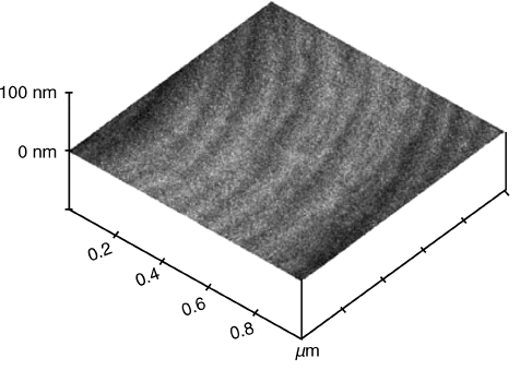
was used to further distinguish atomic scale morphology of the films. Figure 7.11 is a
1 mm 1 mm 3D AFM picture taken from a 0.5 mm thick ZnO film, showing the high
quality of the film. One significant feature is the “flow pattern” composed of well defined
atomic steps on the surface. This indicates that the epitaxial growth progressed with a 2D
growth mode, rather than columnar, 3D growth. The rms roughness of the film is only
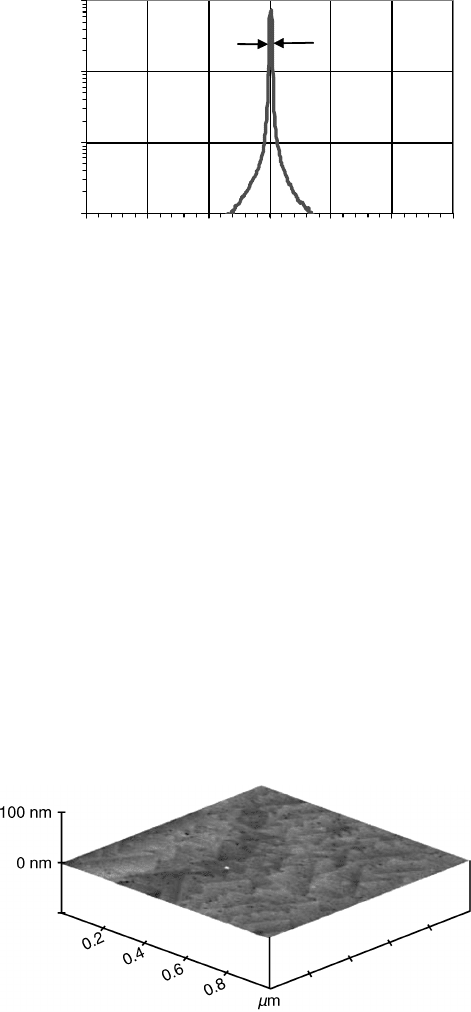
0.23 nm. X-ray rocking curve measurements indicated that the 2D-grown homoepitaxial
films are of high crystallinity. An omega-scan X-ray rocking curve is illustrated in
Figure 7.12 using a logarithmic vertical scale. This rocking curve is a symmetric, single
peak without any appreciable side lobes. The FWHM of these rocking curves have been
measured as narrow as 82 arc-sec, equal to the value measured from the substrate. It is
possible that most of the diffraction signal is from the ZnO substrate (the CuK
a
X-rays can
penetrate through the ZnO epitaxial film). However, no significant dete rioration or
broadening of the curve shape can be observed, suggesting the epitaxial film is of high
crystallinity.
Figure 7.11 AFM picture taken from a ZnO film that is homoepitaxially grown in 2D mode by
MOCVD on an SCVT ZnO substrate
ZnO Homoepitaxy 183
ZnO homoepitaxial films grown in 2D mode by MBE are featureless under the
Nomarski microscope at 1000x magnification. A typical morphology of these films is
shown in the AFM image in Figure 7.13, generated for a 1 mm 1 mm area of a film grown
on an G0001H oriented SCVT ZnO substrate. The image illustrates the full coverage of
the surface by triangular facets. These are different from the “flow pattern” morphology of
MOCVD-grown homoepitaxial films but still represent a 2D growth mode. The step
heights at the edges of the triangular facets are either one or two monolayers. According to
these characteristics, the 3D growth mode often observed in ZnO epitaxial growth has
been completely suppressed. The rms roughness across the 1 mm 1 mm area is 0.15 nm.
The homoepitaxial films have also been evaluated by X-ray diffraction rocking curve
measurements. The (0002) omega-scan X-ray rocking curves (using CuK
a
radiation) show
a single peak at the Bragg diffraction position. Comparing the rocking curves of the ZnO
substrates prior to growth and the Zn O samples after growth (ZnO substrate with a ZnO
X-Ray: Omega Scan
10
100
1000
10000
19
18.5
18
17.5
17
16.5
16
Omega (degree)
Relative Intensity (a. u.)
82”
Figure 7.12 Omega-scan X-ray rocking curve taken from a homoepitaxial film by MOCVD
Figure 7.13 AFM image taken from a homoepitaxial film grown by MBE showing the growth
was in a 2D mode
184 Vapor Transport Growth of ZnO Substrates and Homoepitaxy of ZnO Device Layers

homoepitaxial film), no significant deterioration/broadening of the curve shapes were
observed, suggesting these epitaxial films are also of high crystallinity.
7.5.3 ZnO Homoepitaxial Films on a-plane SCVT ZnO Substrates
Nonpolar growth of ZnO homoepitaxial films was performed on a-plane SCVT ZnO
substrates using MOCVD. Figure 7.1 4 is an AFM image taken from one of the nonpolar
films showing a typical morphology for films of this orientation. It features an in-plane
line structure along the G0001H direction , indicating that ZnO has a selective growth
characteristic along the c-axis.
7.6 Summary
CVT and the SCVT process in particular are capable of producing high crystalline quality,
extremely high purity, conductive, n-type ZnO substrates. In addition, the diameter of the
SCVT growth process is easily scalable for higher volume applications. The surface
preparation techniques and proper homoepitaxial growth parameters have enabled high
quality ZnO epilayers to be grown on the SCVT ZnO substrates. These epilayers are the
precursors to highly efficient optoelectronic devices.
The low cost of starting materials, the ability to grow high quality substrate material at
low cost by SCVT and the benign nature of ZnO all contribute to making ZnO a prime
candidate for high volume production of environmentally friendly optoelectronic devices.
In addition, ZnO has long been touted as a potentially excellent bulk substrate for GaN
epitaxy, especially for GaN-based LEDs and LDs and the techniques to produce high
quality GaN epitaxial films on ZnO substrates have continued to improve.
[30–33]
With the
interest in semi-polar and nonpolar orientations of GaN for increased emission efficiency,
the need for bulk substrates for GaN devices has intensified.
[34–37]
While GaN bulk
substrates have recently become available, their potential production cost is very high
compared with that of bulk ZnO substrates. This makes nonpol ar ZnO substrates for
nonpolar GaN epitaxy very attractive.
Figure 7.14 AFM image of a homoepitaxial film grown on an a-plane ZnO substrate by
MOCVD
Summary 185
Acknowledgement
This work was supported in part by DOE, AFOSR, and ARO.
References
[1] W.W. Piper and S.J. Polich, J. Appl. Phys. 32, 1278 (1961).
[2] V.A. Akimov, M.P. Frolov, Yu.V. Korostein, V.K. Kozlovsky, A.K. Landman, Yu.P. Podmarkov
and A.A. Voronov, Phys. Status Solidi C 3, 1213 (2006).
[3] C.-H. Su, Pro. SPIE 3123, 7 (1997).
[4] A. Micielski and A.J. Szadkowski, Jpn. J. Cryst. Growth 27, 63 (2000).
[5] R. Tena-Zaera, C. Martinex-Tomas, C.J. Gomez-Garcia and V. Munoz-Sanjose, Cryst. Res.
Technol. 41, 742 (2006).
[6] J.T. Mullins, B.J. Cantwell, A. Basu1 Q. Jiang, A. Choubey, A.W. Brinkman and B.K. Tanner,
J. Electron. Mater. 37, 1460 (2008).
[7] J.L. Boone, G. Cantwell, W.C. Harsch, J.E. Thomas and B.A. Foreman, J. Cryst. Growth 139,
27 (1994).
[8] X.H. Yang, J. Hays, W. Shan, J.J. Song, E. Cantwell and J. Aldridge, Appl. Phys. Lett. 59, 1681
(1991).
[9] H.L. Cotal, B.G. Markey, S.W.S. McKeever, G. Cantwell and W.C. Harsch, Physica B 185, 103
(1993).
[10] ZN Technology, unpublished internal data.
[11] M.M. Faktor, I. Garrett and R. Heckingbottom, J. Cryst. Growth 9, 3 (1971).
[12] J. Boone, ZN Technology, unpublished internal report.
[13] A. Reisman, M. Berkenblib, S. A. Chan and J. Angilello, J. Electron. Mater. 2, 177 (1973).
[14] F. T. J. Smith, Appl. Phys. Lett. 43, 1109 (1983).
[15] P. Souletie, S. Bethke, B. W. Wessels and H. Pan, J. Cryst. Growth 86, 248 (1988).
[16] D.C. Look, G.C. Farlow, PakPoom Reunchan, Sukit Limpijumnong, S.B. Zhang and K.
Nordlund, Phys. Rev. Lett. 95, 225502 (2005).
[17] D.C. Look, B.B. Claflin, G. Cantwell, S.-J. Park and G.M. Renlund, in Zinc Oxide – A Material
for Micro- and Optoelectronic Applications, edited by N.H. Nickel and E. Terukov, Springer,
Dordrecht, 2005, Ch. 4.
[18] L. Brillson,Ohio State University, unpublished data.
[19] W. Shan, W. Walukiewicz, J.W. Ager III, K.M. Yu, H.B. Yuan, H.P. Xin, G. Cantwell and J.J.
Song, Appl. Phys. Lett. 86, 191911 (2005).
[20] V. Bhosle, J. T. Prater, F. Yang and D. Burk, J. Appl. Phys. 102, 023501 (2007).
[21] V. Assuncao, E. Fortunato, A. Marques, A. Goncalves, I. Ferreira, H. Aguas and R. Martins,
Thin Solid Films 442, 102 (2003).
[22] H. Kim, Y. Lee, Y. Roh, J. Jung, M. Lee and H. Kwon, 1998 IEEE Ultrasonics Symp. Prc. 1,
323 (1998).
[23] B. Kotlyarchuk, V. Savchuk and M. Oszwaldowski, Cryst. Res. Technol. 40, 1118 (2005).
[24] C.-H. Lu, Yu-H. Huang and A. Dhobale, Jpn. J. Appl. Phys. 45, 228 (2006).
[25] Y. Cao, L. Miao, S. Tanemura, M. Tanemura, Y. Kuno, Y. Hayashi and Y. Mori, Jpn. J. Appl.
Phys. 45, 1623 (2006).
[26] J. Zhong, H. Chen, G. Saraf, Y. Lu, C. K. Choi, J. J. Song, D. M. Mackie and H. Shen,
Appl.
Phys. Lett. 90, 203515 (2007).
[27] B. P. Zhang, N. T. Binh, K. Wakatsuki, Y. Segawa, Y. Yamada, N. Usami, M. Kawasaki and
H. Koinuma, Appl. Phys. Lett. 90, 4098 (2004).
[28] Weizhong Xu, Zhizhen Ye, Liping Zhu, Yujia Zeng, Liu Jiang and Binghui Zhao, J. Cryst.
Growth 277, 490 (2005).
[29] J. Zhang, G. Cantwell, C. K. Choi, J. J. Song, J. Zhong, H. Cheng and Y. Lu, in Procedings of
GOMACTECH-07, Lake Buena Vista, FL, 2007, paper #9-3.
186 Vapor Transport Growth of ZnO Substrates and Homoepitaxy of ZnO Device Layers
[30] T. Ohgaki, N. Ohashi, T. Ohnishi, H. Haneda, M. Lippmaa and A. Yasumori, J. Ceram. Soc.
Jpn. 115, 414 (2007).
[31] A. Kobayashi, S. Kawano, K. Ueno, J. Ohta, H. Fujika, H. Amanai, S. Nagao and H. Horie,
Appl. Phys. Lett. 91, 191905 (2007).
[32] A. Kobayashi, S. Kawano, Y. Kawaguchi, J. Ohta and H. Fujioka, Appl. Phys. Lett. 90, 041908
(2007).
[33] K Ueno, A. Kobayashi, J. Ohta and H. Fujioka, Appl. Phys. Lett. 90 , 141908 (2007).
[34] H. Masui, H. Yamada, K. Iso, J.S. Speck, S. Nakamura and S.P. DenBaars, J. Soc. Inf. Display
16, 571 (2008).
[35] Y. Tsuda, M. Ohta, P.O. Vaccaro, S. Ito, S. Hirukawa, Y. Kawaguchi, Y. Fujishiro, Y. Takahira,
Y. Ueta, T. Takakura and T. Yuasa, Appl. Phys. Express 1, 011104 (2008).
[36] A. Tyagi, H Zhong, N.N. Fellows, M. Iza, J.S. Speck, S.P. DenBaars and S. Nakamura, Jpn. J.
Appl. Phys. 46, L129 (2007).
[37] B.A. Haskell, S. Nakamura, S.P. DenBaars and J.S. Speck, Phys. Status Solidi B 244, 2847
(2007).
References 187

8
Growth Mechanisms and Properties
of Hydrothermal ZnO
M. J. Callahan
1,3
, Dirk Ehrentraut
2
, M. N. Alexander
3
and Buguo Wang
4
1
Teleos Solar, Hanson, MA, USA
2
Institute of Materials Research (IMR), Tohoku University, Aoba-ku, Sendai, Japan
3
Air Force Research Laboratory, Sensors Directorate, Hanscom AFB, MA, USA
4
Solid State Scientific Corp., Nashua, NH, USA
8.1 Introduction
Because of its direct band gap at 3.4 eV and large excitonic binding energy (60 meV), zinc
oxide (ZnO) has attracted considerable interest for possible applications in emitter and
detector applications in the blue to ultraviolet (UV) portion of the spectrum.
[1]
ZnO also has
many other unique properties such as the ability to alloy with Mg or Cd in fabrication of
quantum wells, resistance to radiation damage, high voltage breakdown strength, and high
electron saturation velocity.
[2]
In addition, ZnO also has large piezoelectric and acousto-optic
coefficients,
[3]
and with appropriate doping it can have ferroelectric, magnetic, and nonlinear
electrical properties. It exhibits strong two-photon absorption and a very high optical damage
threshold, rendering it attractive for saturable absorber applications.
[4]
ZnO powder, polycrystalline, and single crystal material have been and will be integral
elements in such applications as low voltage varistors, surge protectors , photocatalysts,
chemical detectors, biological and medical processing, phosphors, visible-UV detectors
and emitters, and high power electronics.
A large, low cost ZnO substrate would speed development of ZnO-based optoelectron-
ics. ZnO boules up to 50 mm in diameter and 10 mm thick have been grown by vapor phase
Zinc Oxide Materials for Electronic and Optoelectronic Device Applications, First Edition.
Edited by Cole W. Litton, Donald C. Reynolds and Thomas C. Collins.
© 2011 John Wiley & Sons, Ltd. Published 2011 by John Wiley & Sons, Ltd. ISBN: 978-0-470-51971-4
transport,
[5]
and melt-grown wafers 50 mm diameter are now also available.
[6]
Both
processes typically yield wafers with dislocation densities of 10
4
–10
5
cm
2
.
Hydrothermal growth has certain advantages over other methods in produc ing high purity,
low defect-density, and small uniform grain size crystallites (for powder) because of lower
growth temperature and slower growth rates.
[7–11]
Hydrothermal ZnO wafers have been
produced with dislocation densities as low as 100 cm
2
and carrier concentrations as low as
2 10
12
.
[12]
Early interest in single crystal ZnO focused on piezoelectric transducers; for this
purpose, large hydrothermal crystals were grown in the 1960s.
[13–15]
Renewed interest arose
because of ZnO’s potential as an isostructural, nearly lattice-matched substrate for group III
nitride semiconductor device structures.
[16]
Advances in fabricating ZnO and ZnMgO
quantum wells on sapphire that exhibit strong optically stimulated UVemission have further
driven demand for development of ZnO subst rates.
[17]
This review focus es on the hydrothermal growth of single crystals of ZnO, including
pertinent information on microcrystalline growth when it provides insight on the growth
kinetics of larger crystals. Phase stability, solubility, growth kinetics, and impurity
incorporation are discussed. Electrical and optical properties are reviewed with special
interest in the effects of crystalline anisotropy. Ph enomena related to etching and polishing
are also discussed.
8.2 Overview of Hydrothermal Solution Growth
Byrappa and Yoshimura define hydrothermal growth as “any heterogeneous chemical
reaction in the presence of a solvent (whether aqueous or non-aqueous) above room
temperature at an pressure greater than 1 atm in a closed system”.
[8]
Hydrothermal crystal
growth offers several advantages over better-known methods such as melt growth. Hydro-
thermal growth is a low temperature process, which often makes possible the growth of
materials that are difficultorimpossible to melt, or materials which, in solidifying froma melt
and cooling down, would undergo phase changes (bec ause of such changes, a-quartz cannot
be grown from the melt). Low temperature hydrothermal growth can also minimize or
eliminate the incidence of temperature-induced point defects, as illustrated by growth of
Bi
12
SiO
20
,
[18]
and it can produce large amounts of material (over 4000 kg of single crystal
quartz has been produced in a single run).
[8]
Some disadvantages of hydrothermal growth are
the low growth rate and initial capital equipment costs, but these are offset by the ability to
growmultiplecrystalsin asinglerunandthe longlifetimesof theautoclaves. Additionally,the
labor requirements are minimal due to the simplicity of the autoclaves where closed system
crystal growth occurs for long periods of time at steady-state temperatures and pressures.
An in depth review of hydrothermal technol ogy is covered in several references.
[7,8]
8.3 Thermodynamics of Hydrothermal Growth of ZnO
8.3.1 Solubility of ZnO in Various Aqueous Media
In hydrothermal growth a “nutrient”, often the compound one intends to grow, is dissolved
in an aqueous medium. The dissolved compound may form intermediate complexes or
species such as hydrides, hydrates, hydroxides, or oxides in solution. In hydrothermal
190 Growth Mechanisms and Properties of Hydrothermal ZnO
growth, convective circulation and/or diffusion of these species throughout the aqueous
medium provides the primary mechanism for synthesizing crystalline compounds.
A hydrothermal growth system is designed to bring the soluble species into a region
of the aqueous medium where a change in conditions – e.g. in temperature, solvent
composition, pH, or pressure – promotes crystal growth by bringing the soluble species
into supersaturation. Supersaturation is defined as the amount of material in solution above
the equilibri um concentration for a substance under a specific set of conditions. A
supersaturated species must eventually come out of solution – hopefully as the desired
compound (e.g. ZnO) – until equilibrium state (saturation) is achieved.
The first requirement for hydrothermal growth follows immediately from the forego-
ing discussion: the solubility of nutrient in the solvent medium must be adequate for
growth. Low solubility will result in low growth rates; excessively high solubility will
result in polycrystalline growth or spontaneous nucleation, which prohibits growth of
low defect-density single crystals. Typically, the nutrient should be 1–10 wt% soluble in
the solvent. Solubility can be increased by adding a proper complexing agent (miner-
alizer). Most mineralizers used in hydrothermal growth change the pH of the solvent,
making the solvent either acidic or alkaline, i.e. increasing the number of H
þ
or OH
ions that attack the nutrient material in aqueous solutions. For ZnO, a solubility of
approximately 5 wt% in alkaline solution yields high quality single crystals at reas on-
able growth rates.
The majority of compounds that can be dissolved in solutions will have a change in
solubility when the temperature of the solution is raised or lowered. Therefore, most
solution growth methods, including the hydrothermal method, use a change in temperature
at the seed interface to create supersaturation. Thus, the second requirement of hydro-
thermal growth is that the solubility of the compound has an adequate range of temperature
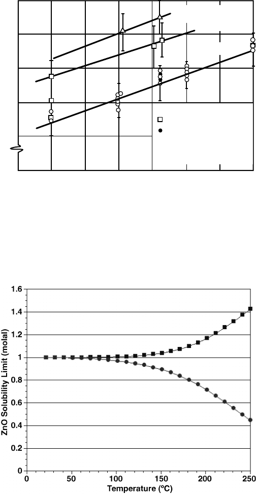
dependence for high growth rates. The solubility of ZnO in an OH
alkaline medium is
shown in Figure 8.1.
[19]
Note that solubility increases with temperature. This is called
normal solubility or forward solubility.
ZnO is an amp hoteric oxide, meaning it acts as an acid in alkaline solutions and as a
base in acidic solutions. It is possible to grow hydrothermal ZnO in an acidic solution as
well as the alkaline solutions shown in Figure 8.1. McCandlish and Uhrin recently studied
the solubility of ZnO in an acidic medium and grew ZnO at 100–250
C, with growth rates
up to 0.25 mm day
1
.
[20]
Figure 8.2 illustrates the solubility in acidic regimes. The squares
signify 2 molal aqueous nitric acid and the circles signify a proprietary acidic solution.
Note that the nitric acid solution exhibits normal solubility, whereas the proprietary
solution exhibits decreasing solubility with increasing temperature (retrograde solubility).
To grow ZnO crystals under conditions of normal solubility the seed is placed in a colder
region than the source material (see Section 8.4.2); to grow under conditions of retrograde
solubility, the seed is placed in the hotter region.
8.3.2 ZnO Phase Stability in H
2
O System
A third requirement for hydrothermal growth is that the desired compound is thermody-
namically favored at the growth interface. If an oxide like ZnO is desired, the hydride,
hydroxide or hydrate cannot be thermodynamically favored for a given mineralizer,
Thermodynamics of Hydrothermal Growth of ZnO 191
9.07 m KOH
1380 BARS
270 BARS
150
7
6
5
4
3
0
200 300250 400350
Temperature (ºC)
Solubility (wt%)
450 500
OTHER POINTS AT
550 BARS
6.24 m NaOH
6.47 m KOH
Figure 8.1 Solubility of ZnO vs temperature in aqueous NaOH and KOH solutions
[19]
.
Reprinted from R.A. Laudise, E.D. Kolb, American Mineralogist (USA) 48 [3] 642. Copyright
(1963) with permission from the Mineralogical Society of America
Figure 8.2 Normal solubility of ZnO in 2 molal nitric acid (squares) and retrograde solubility of
ZnO in a proprietary acid solution (circles). Reprinted from Handbook of Crystal Growth,
Editors Govindhan Dhanaraj, Kullaiah Brrappa, Vishwanath Prasad, and Michael Dudley,
Publisher Springer 2010, ISBN: 978-3-540-74182-4, Chapter 19 Hydrothermal and Ammo-
nothermal Growth of ZnO and GaN pp 655–689, Figure 19.6
192 Growth Mechanisms and Properties of Hydrothermal ZnO