Henini M. Handbook of Self Assembled Semiconductor Nanostructures for Novel devices in Photonics and Electronics
Подождите немного. Документ загружается.

Quantum Dot Structures for Multi-band Infrared and Terahertz Radiation Detection 669
can be further reduced using a DWELL structure. Compared to DWELL detectors, T-QDIPs exhibit
lower dark current due to dark current blocking by the double-barrier system. As a result, T-QDIPs
have the potential to achieve the highest possible operating temperature. Additionally, photocur-
rent fi ltering by means of resonant tunnelling in T-QDIPs offers a solution for low quantum effi -
ciency, which has been observed in other QD-based devices. Quantum effi ciency can be increased
further through resonant cavity enhancement [76–78] , which increases the absorption in the
active region without increasing the dark current. In addition, several other important properties
of T-QDIPs include the tunability of the operating wavelength and the multicolour (band) nature
of the photoresponse based on different transitions in the structure. The operating wavelength can
be tailored by changing the device parameters of the QW, QD, and double-barrier system. Utilizing
transitions between the energy levels of the QD and the energy levels of the QW, it is possible to
obtain detectors with multiple distinct response peaks.
22.3.1 Theoretical background and T-QDIP structure
Incorporating resonant tunnelling into QDIP structure design allows for the reduction of the dark
current without reducing the photocurrent, thus leading to high performance. A typical T-QDIP
consists of InGaAs QDs embedded in an AlGaAs/GaAs QW, which is then coupled to an AlGaAs/
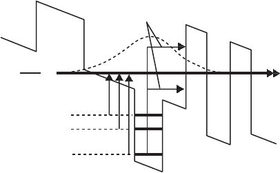
InGaAs/AlGaAs double-barrier system. The conduction band profi le of a T-QDIP structure under
an applied reverse bias is shown in Fig. 22.9 . Pulizzi et al. [79] have reported resonant tunnel-
ling phenomena for a similar QD-based structure coupled with a double barrier. The photocur-
rent generated by a transition from a state in the QD ( E
1
, E
2
or E
3
) to a state in the QW, which is
coupled with a state in the double-barrier system, can be collected by resonant tunnelling. In this
discussion, the energy state in the QW is denoted as the resonant state, E
r
, since it is associated
with resonance tunnelling. The double-barrier system blocks the majority of carriers contributing
to the dark current (carriers excited to any state other than the resonant state in the QW). It can
be shown that the tunnelling probability is near unity for carriers excited by radiation with energy
equal to the energy difference between the QD ground state and the resonant state.
AIGaAs barrier
( 0 meV)
Dark
current
E
r
E
3
E
2
E
1
InGaAs QD
Photo/curren
t
AIGaAs/InGaAs/AIGaAs
double barrier
Figure 22.9 Schematic diagram of the conduction band profi le of a T-QDIP structure under a bias. E
1
, E
2
and E
3
are the energy level positions in the QD with respect to the resonant-state E
r
. Only the carriers excited to the resonant
state contribute to the photocurrent. Modifi ed after [43] .
The fi rst step in designing a T-QDIP is the calculation of the QD energy levels using the 8-band
k p model [70] . This model uses the strain in the QD, which is calculated using the valence force
fi eld (VFF) model. VFF model has proven successful in calculating the strain tensor in self-assembled
QDs. The size of the QD and the confi nement potential should be designed such that the required
spacing between energy levels can be obtained. For example, in order to design a two-colour
T-QDIP with response peaks at 5 and 10 μ m, the ground and fi rst excited states in the QD
(labelled as E
1
and E
2
in Fig. 22.9 ) should be 248 and 124 meV below the resonant-state energy.
The energy spacing between states E
2
and E
1
is equal to 124 meV. Theoretical calculations
CH022-I046325.indd 669CH022-I046325.indd 669 6/27/2008 3:51:34 PM6/27/2008 3:51:34 PM
670 Handbook of Self Assembled Semiconductor Nanostructures for Novel Devices in Photonics and Electronics
indicate that the energy difference between the ground and fi rst excited state in small InAs/GaAs
QDs, with a height of 60 Å and a width of 110 Å, is approximately 124 meV. The width and the
confi nement potential of the QW are adjusted to obtain the resonant state at 248 meV above E
1
state (at 124 meV above E
2
state). The doping concentration in the QDs should be suffi ciently
high so that both states in the QD are fi lled with ground-state electrons. The energy states in the
QW, including the presence of the wetting layer and the double-barrier system, are calculated by
solving the one-dimensional Schrödinger equation. The transmission probability for the double-
barrier structure is calculated using the transfer matrix method [80] .
The double-barrier system (AlGaAs/InGaAs/AlGaAs) is integrated with each QD layer of the
QDIP, and is designed such that the resonant state coincides with a bound state in the double-
barrier system under certain bias conditions. In this way, a higher potential barrier for thermal
excitations can be introduced, while the photoexcitation energy remains very low. Due to the
energy-dependent tunnelling rate of the double-barrier system, the dark current resulting from
carriers with a broad energy distribution is suppressed. Thus the dark current can be signifi -
cantly reduced, particularly at high temperatures.
The intersubband absorption coeffi cient of a photon with energy ω in a QD layer can be
expressed as [5] :
αω
π
εω
ω() | |()
e
ncmV
ap N
av
fi
fi
2
00 0
2
2
1
∑
(22.6)
where V
av
is the average QD volume, a is the polarization of the incident light, p
fi
is the momen-
tum matrix element between energy states, and N ( ω ) is the electron density of states. The
Gaussian inhomogeneous broadening due to the fl uctuations in QD size, N ( ω ), is:
N
E
fi
() exp
()
ω
πσ
ω
σ
1
2
2
2
2
⎧
⎨
⎪
⎪
⎩
⎪
⎪
⎫
⎬
⎪
⎪
⎭
⎪
⎪
(22.7)
where E
fi
is the energy separation between states and σ is the linewidth of the transition. The
momentum matrix element is calculated from the QD wavefunctions, which can be obtained
from the 8-band k p model. The spectral response of the detector is characterized by peak wave-
length ( λ
p
), peak responsivity ( R
p
), and the peak quantum effi ciency ( η
p
). Responsivity is given by
R q η λ / hc , where q is the electron charge, λ is the wavelength, h is the Planck constant and c is
the speed of light. Quantum effi ciency can be calculated from the absorption coeffi cient (from Eq.
22.6) and the thickness of the absorption region.
In order to achieve background-limited infrared performance (BLIP) conditions at high tem-
peratures, the detector should exhibit an extremely low dark current density. A T-QDIP designed
to have strong resonant tunnelling is capable of achieving high BLIP temperatures. The dark
current, I
d
, of a T-QDIP structure at a bias, V , is given [74] by:
IV evVn VA
dem
() () ()
(22.8)
where A is the device area, v and n
em
(given by Eqs 22.9 and 22.10) are the average electron drift
velocity in the barrier material and the concentration of electrons excited out of the QD, respec-
tively. The electron drift velocity is given by:
vV
FV
FV
v
s
()
()
()
μ
μ
1
⎛
⎝
⎜
⎜
⎜
⎜
⎞
⎠
⎟
⎟
⎟
⎟
2
(22.9)
where μ is the electron mobility, F is the electric fi eld, and v
s
is the electron saturation velocity.
The excited electron density from the QD is given by :
nV NEfETEVdE
em
() ()()(, )
∞
∞
∫
(22.10)
CH022-I046325.indd 670CH022-I046325.indd 670 6/27/2008 3:51:35 PM6/27/2008 3:51:35 PM
Quantum Dot Structures for Multi-band Infrared and Terahertz Radiation Detection 671
where f ( E ) is the Fermi–Dirac distribution function, T ( E,V ) is the tunnelling probability calculated
by the transfer matrix method [80] , and N ( E ) is the density of states, which is given by the follow-
ing equation:
NE
N
L
EE
m
Lh
HE
d
p
fi
i
p
()
()
(
21
2
2
4
2
2
2
πσ
σ
π
exp
*
⎧
⎨
⎪
⎪
⎩
⎪
⎪
⎫
⎬
⎪
⎪
⎭
⎪
⎪
∑
EE
h
mEEHEE
WCC
)() ()
()
82
3
32
π
*
/
(22.11)
where the fi rst term is the density of states of the QD state and N
d
is the surface density of QDs.
The second term is the density of the wetting layer states, where E
W
is the wetting layer state, and
H( x ) is a step function with H( x ) 1 for x 0 and H( x ) 0 for x 0. The third term describes
the density of states in the barrier material, where E
C
is the conduction band edge of the barrier
material.
As shown in Fig. 22.9 , the carriers excited to any state other than the resonant state are
blocked by the tunnel barriers. However, for effi cient dark current blocking, the broadening of
the resonant state has to be at a minimum. That is, the resonant state should be strongly bound.
Basic parameters should be adjusted so that the tunnelling probability remains close to unity
and the carrier escape lifetime is smaller than the carrier recombination lifetime. The Fermi level
in the QD (hence QD ground state) should be below the band edge of the QW; however, adjust-
ing the ground state will change the energy difference between the QD ground state and the res-
onant state, which will affect the peak response wavelength. Thus, all these factors need to be
taken into account to design an optimized detector exhibiting low dark current.
22.3.2 Two-colour room temperature T-QDIPs
As reported by Bhattacharya et al . [43] a T-QDIP structure (MG386) was grown by MBEs and
then characterized using I–V , spectral response, and noise measurements. The results demon-
strated the detector’s ability to operate at room temperature due to resonant tunnelling phenom-
enon present in the structure. The detector showed a two-colour response at wavelengths of ⬃ 6
and ⬃ 1 7 μ m up to room temperature. A detailed explanation of the device structure, spectral
response and device performance are given in following sections.
22.3.2.1 T-QDIP structure and experiment
The T-QDIP structure MG386 (reported by Bhattacharya et al .) is schematically shown in Fig.
22.10 . Self-organized In
0.1
Ga
0.9
As QDs were grown on a GaAs substrate. A stack of Al
0.3
Ga
0.7
As/
In
0.1
Ga
0.9
As/Al
0.3
Ga
0.7
As layers serve as the double-barrier system. The conduction band
profi le of this T-QDIP structure under an applied reverse bias is shown in Fig. 22.9 . The GaAs
and AlGaAs layers were grown at 610°C and the InGaAs or InAlAs QD layers were grown at
500°C. Vertical circular mesas for top illumination were fabricated by standard photolithogra-
phy, wet chemical etching and contact metallization techniques. The n -type top ring contact
and the n -type bottom contact were formed by evaporated Ni/Ge/Au/Ti/Au with a thickness
of 250/325/650/200/2000 Å. The radius of the optically active area is 300 μ m. Samples with
devices to test were mounted on chip carriers using silver epoxy. Then electrical contacts were
made by bonding gold wires from devices to the chip carrier leads. Characterization techniques
used are explained in section 22.2.2.
22.3.2.2 Dark current measurements
Dark I–V measurements for MG386, at different temperatures ranging from 80 to 300 K, are
shown in Fig. 22.11a . Positive (or negative) bias denotes positive (or negative) polarity on the
top contact. A comparison of the dark current density between DWELL (1299) [9] and T-QDIP
(MG386) detectors at 80 K is shown in Fig. 22.11b . Dark current densities at a bias of 2 V
are 3 1 0
1
and 1.8 1 0
5
A / c m
2
for DWELL and T-QDIP, respectively. The reduction in dark
CH022-I046325.indd 671CH022-I046325.indd 671 6/27/2008 3:51:35 PM6/27/2008 3:51:35 PM
672 Handbook of Self Assembled Semiconductor Nanostructures for Novel Devices in Photonics and Electronics
GaAs n
contact
40 Å AI
0.1
Ga
0.9
As (i)
30 Å AI
0.3
Ga
0.7
As (i)
30 Å AI
0.3
Ga
0.7
As (i)
400 Å GaAs (i)
GaAs n
contact
S.I. GaAs substrate
40 Å In
0.1
Ga
0.9
As (i)
10 Å GaAs (i)
40 Å GaAs (i)
In
0.4
Ga
0.6
As QDs (i)
10
Figure 22.10 A schematic heterostructure of a T-QDIP grown by MBE. InGaAs QDs are placed in a GaAs QW.
The AlGaAs/InGaAs/AlGaAs layers serve as a double-barrier system to decouple the dark and photo currents. The
letter “ i ” stands for intrinsic. After [43] .
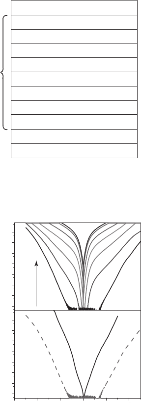
Figure 22.11 (a) Dark current density of the T-QDIP sample (MG386) as a function of bias in the temperature
range 80–300 K. (b) A comparison of the experimental dark current density between a DWELL detector (1299)
and a T-QDIP (MG386) at 80 K. The reduction of the dark current in T-QDIP is attributed to dark current blocking
by the double-barrier system. Modifi ed after [43] .
10
0
10
2
10
2
10
0
10
4
10
4
10
6
10
6
6
024
4
2
Bias (V)
DWELL
(1388)
80 K
(a)
300 K
280
240
160
120
80
200
Dark current density (A/cm
2
)
T-QDIP
(MG386)
(b)
current of the T-QDIP is associated with the double-barrier system in the structure. Moreover,
dark current densities for MG386 at a bias of 1 V were 0.21, 0.96, and 1.55 A/cm
2
at 240, 280
and 300 K, respectively. These dark current density values are lower than the dark current val-
ues of other IR detectors operating in comparable wavelength regions at the same temperature.
Based on the dark current variation as a function of bias, negative conductance peaks were not
visible even though resonant tunnelling takes place in the structure. This observation can be
expected for T-QDIPs since sequential resonant tunnelling through ground state is not possible.
In T-QDIP structures, there is no coupling between the QD ground state and states in the double
CH022-I046325.indd 672CH022-I046325.indd 672 6/27/2008 3:51:35 PM6/27/2008 3:51:35 PM
Quantum Dot Structures for Multi-band Infrared and Terahertz Radiation Detection 673
barrier (unlike in superlattice structures [81] ). Also, each active region of the T-QDIP is separated
by a thick spacer layer (400 Å GaAs), which does not allow any signifi cant coupling between two
active regions (two periods). Thus, I–V curves are not expected to display negative conductance
regimes. Furthermore, it is important to underline the thin AlGaAs barriers (30 or 40 Å) on both
sides of the QW. Even though the double barrier is placed only on one side of the QW (on the right
side according to Fig. 22.9 ), tunnelling through the single barrier on the opposite side (on the left
side of the QW) is also possible. However, the transmission through this barrier is lower compared
to that through the double barrier. Thus, an asymmetric I–V characteristic was observed.
22.3.2.3 Spectral responsivity
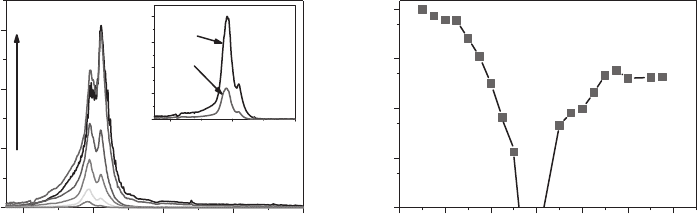
The spectral response of MG386 at 80 K under different bias values is shown in Fig. 22.12a ,
and the variation of the peak responsivity at 6.2 μ m is shown in Fig. 22.12b . Based on calcula-
tions, the allowed confi ned energy states in the QD E
1
, E
2
, and E
3
are located at 161, 103,
and 73 meV with respect to the resonant state (see Fig. 22.9 ). Thus, the peak at ⬃ 6 μ m is due to
transitions from the ground state of the QD to the resonant state in the structure, which is consist-
ent with the calculated energy spacing between corresponding states ( Δ E 161 meV). The peak
responsivity and the conversion effi ciency (the product of quantum effi ciency and the photocon-
ductive gain) of the 6 μ m peak at 80 K and 4.5 V are ⬃ 0.75 A/W and 16%, respectively. Under
reverse bias (top contact is negative), the photoexcited electrons tunnel through the double barrier
by resonant tunnelling. Similarly, under forward bias photoexcited electrons tunnel through the
single barrier (on the opposite side of the double-barrier system). Due to the variations in trans-
mission through the single and double barriers, the response under reverse bias is signifi cantly
higher than the response under forward bias, as evident from Fig. 22.9 . However, the responsiv-
ity shows a strong dependence on the applied bias in both positive and negative directions. This
behaviour is attributed to resonant tunnelling similar to that of double-barrier superlattice struc-
tures [72, 82] . Applying a bias across the structure can fi ne-tune the alignment of the bound state
in the QW (resonant state) and the bound state in the double-barrier system, allowing for resonant
tunnelling conditions. The observed bias dependence of the responsivity indicates that resonant
conditions are satisfi ed over a considerable range of applied bias voltages. This behaviour could be
associated with thin barriers and the broadening of the energy states ( δ E ) in the system.
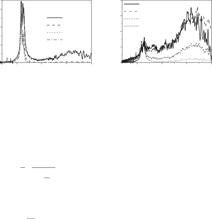
The spectral response of the MG386 detector under a 2 V bias at different temperatures in
the range of 80–300 K is shown in Fig. 22.13a and b. Two distinct peaks centred around ⬃ 6
and ⬃ 1 7 μ m were observed at high temperatures, and a weak response around 11 μ m was
also present. The peak at 17 μ m results from transitions between the second excited state of
the QD and the resonant state ( Δ E 73 meV). The linewidth is ⬃ 26 meV, which corresponds
Figure 22.12 (a) Bias dependence of the spectral responsivity of T-QDIP (MG386) at 80 K from 1.5 to 4 V.
The inset shows the responsivity at low bias values (from 0.25 to 1.5 V). (b) Variation of the peak responsivity
with applied bias at 80 K.
0.6
10
0
10
2
10
3
10
4
6
4 2
0
2
4
6
10
1
0.0
0.2
0.4
4121086
Bias (V)
Wavelength (m)
T 80 K
T 80 K
468
20
5
0
15
10
1.5 V
1.0 V
4 V
2.5 V
2.0 V
1.5 V
3.5 V
3.0 V
(a)
Wavelength (m)
Responsivity (mA/W)
(b)
Responsivity (mA/W)
Responsivity (A/W)
λ
p
6.2 μm
CH022-I046325.indd 673CH022-I046325.indd 673 6/27/2008 3:51:36 PM6/27/2008 3:51:36 PM
674 Handbook of Self Assembled Semiconductor Nanostructures for Novel Devices in Photonics and Electronics
to the inhomogeneous broadening of QD states at 300 K. Due to the symmetry of QD geome-
try, excited states have a higher degeneracy (8) than the ground state (2). The carrier density in
excited states increases with increasing temperature, as compared to that in the ground state.
As a result, the 17 μ m peak was dominant above 200 K, as evident from Fig. 22.13 . The weak
response at ⬃ 1 1 μ m corresponds to the energy separation between the fi rst excited QD state and
the resonant state (Δ E 102 meV).
0.06
0.02
0.20
0.00
0.05
0.10
0.15
0.04
300 K
280 K
240 K
200 K
200 K
160 K
120 K
80 K
5101520
Wavelength (m)
5101520
Wavelength (m)
V 2 V V 2 V
(a)
Responsivity (A/W)
(b)
Responsivity (A/W)
Figure 22.13 Spectral responsivity of T-QDIP (MG386) in the temperature range (a) 80–200 K, and (b) 200–
300 K under a 2 V bias. Two distinct peaks centred around ⬃ 6 and ⬃ 1 7 μ m can be observed at high temperatures,
and a weak response around 11 μ m is also visible. Modifi ed after [43] .
22.3.2.4 Noise measurements and detectivity
The noise current spectra of QWIPs [83, 84, 85] have been reported in the literature. In general,
the total noise current is a contribution of Johnson noise, 1/ f noise, and generation–recombination
noise ( g–r ) components. However, QWIPs [83] and QDIPs [86] are expected to show very low 1/ f
noise characteristics. The frequency dependent noise spectrum, which is due to 1/ f and generation–
recombination noise components, has the form [87, 88] :
Sf C
B
f
f
f
c
()
A
1
2
⎛
⎝
⎜
⎜
⎜
⎜
⎞
⎠
⎟
⎟
⎟
⎟
(22.12)
where A , B , and C are constants. The cut-off frequency, f
c
, is given by f
c
1 / 2 π τ where τ is the
electron lifetime, which is given by:
τ ∝
⎛
⎝
⎜
⎜
⎜
⎞
⎠
⎟
⎟
⎟
⎟
T
E
kT
A
2
exp (22.13)
where T is the temperature, k is the Boltzmann constant and E
A
is the activation energy of the
thermally activated trap level. Noise current density spectra are used to determine the varia-
tion of τ with temperature. Based on Eq. 22.13, the plot of log( τ / T
2
) against 1/ T would result
in a straight line with a slope of E
A
/ k , which can be used to calculate the activation energy.
Furthermore, the electronic states, carrier capture, and carrier transport properties in a QD-
based structure have been studied [89] using capacitance–voltage spectroscopy [90, 91] and
deep-level transient spectroscopy [92, 93] . A strong negative capacitance phenomenon, which
is originated from carrier capture and emission at interface states, has been observed in HIWIP
[94] and QWIP [95] detector structures.
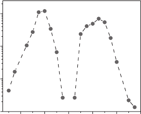
The specifi c detectivity ( D *) of the MG386 detector (reported by Bhattacharya et al. [43] ) at
different temperatures and applied biases was obtained from the measured peak responsivity
and noise density spectra, as described in section 22.2.2. At 80 K and under a bias of 2 V, the
CH022-I046325.indd 674CH022-I046325.indd 674 6/27/2008 3:51:37 PM6/27/2008 3:51:37 PM
Quantum Dot Structures for Multi-band Infrared and Terahertz Radiation Detection 675
maximum D * was found to be 1.2 1 0
10
cmHz
1
/
2
/W. The variation in D * at 6.2 μ m with chang-
ing bias at 80 K is shown in Fig. 22.14 . The rate of increasing noise current with increasing bias
was much higher than the rate of increasing responsivity with increasing bias, resulting in lower
D * at higher bias voltages (beyond 2 V). This variation in D * as a function of bias is expected for
a typical photodetector. The value of D * a t 1 7 μ m and 300 K was of the order of 10
7
cmHz
1
/
2
/W,
and with some redesigning of the device heterostructure, a higher D * can be obtained for the
same conditions.
10
10
10
9
10
8
10
7
4 20246
Bias (V)
D* (cm Hz
0.5
/W)
λ 6.2 m
T 80 K
Figure 22.14 Variation of detectivity of the T-QDIP (MG386) at 6.2 μ m as a function of bias at 80 K. The rate
of increasing noise current with bias is much higher than the rate of increasing responsivity with bias, resulting in
lower D * at higher bias voltages (above 2 V ) .
22.3.3 T-QDIPs for terahertz radiation detection
With an increasing interest in the terahertz region of the spectrum (0.1–3.0 THz), there is a need
for terahertz detectors exhibiting low dark current and high operating temperatures for appli-
cations in imaging, communication, security and defence. The primary challenge in developing
terahertz detectors is the reduction of dark current (due to thermal excitations) associated with
terahertz detection mechanisms in the device structure. At the present time, terahertz detectors
such as Ge BIB detectors [96] , photoconductors triggered by femtosecond laser pulses [97] , QW
detectors [98] , HIWIP detectors [99] , HEIWIP detectors [100] , and thermal detectors, such as
bolometers and pyroelectric detectors, are being studied. However, all of these detectors operate
at low temperatures. A typical detector structure, in which the transitions leading to terahertz
detection occur between two electronic states with an energy difference of Δ E ( ⬃ 4.1 meV for
1 THz), would not be suitable for high-temperature terahertz detection since the dark current due
to thermal excitations become dominant even at 77 K due to the small Δ E . A T-QDIP structure
[73] , in which the photocurrent is selectively collected while the dark current is blocked, can be
adjusted to obtain terahertz response, thus offering a suitable platform for high operating tem-
perature terahertz detectors.
A schematic diagram of a T-QDIP terahertz detector (MG764), reported by Su et al. [73] , is
shown in Fig. 22.15 . The heterostructure was grown by MBE on (001)-oriented semi-insulating
GaAs substrate. The GaAs and AlGaAs layers were grown at 610°C and the rest of the structure
was grown at 500°C. The top and bottom GaAs contact layers were n -doped with Si to a level
of 2 1 0
18
c m
3
. Mesa-shaped vertical n-i-n devices for top illumination were fabricated by
standard photolithography, wet chemical etching, and contact metallization techniques. The top
and bottom n -type contacts were formed by evaporated Ni/Ge/Au/Ti/Au (thickness 250/325/
650/200/2000 Å, respectively) followed by annealing. In order to obtain a transition leading to a
response in terahertz region, the excited states in the QD were pushed towards the resonant state
CH022-I046325.indd 675CH022-I046325.indd 675 6/27/2008 3:51:37 PM6/27/2008 3:51:37 PM

676 Handbook of Self Assembled Semiconductor Nanostructures for Novel Devices in Photonics and Electronics
by forming smaller QDs. The QDs were doped to raise the Fermi level so that photoexcitations take
place from an upper state in the QD to the resonant state. In order to reduce QD size, In
0.6
Al
0.4
As
was used instead of InGaAs because the Al-containing islands (QDs) are smaller in size compared
to InAs islands due to the smaller migration rate of Al adatoms on the growing surface during
epitaxy.
22.3.3.1 Growth of “ small ” quantum dots by MBE
The typical size of the near-pyramidal InAs/GaAs self-organized QDs [9, 19] is ⬃ 60–70 Å
(height)/ ⬃ 200–250 Å (base), and QD density varying between the range 5 and 10 1 0
10
c m
2
.
Typical electron intersublevel energy separation in such QDs ranges between 40 and 80 meV.
Based on calculated results, a large energy spacing ( ⬃ 124 meV) between the QD ground and fi rst
excited states can be obtained using smaller QDs. Smaller QDs also provide a large QD density
for the same amount of adatom change, which increases the absorption of radiation. QD size is
reduced by inhibiting growth kinetics on the surface. This can be done either by growing QDs on
an Al-containing material or by incorporating a small amount of Al into the QD material. The
presence of Al reduces the adatom migration lengths on the growing surface (insuffi cient kinetics),
resulting in smaller QDs. During the investigation of terahertz T-QDIP operating at high tempera-
tures reported by Su et al. [73] , the QD size was considerably reduced to 40 Å (height) and 130 Å
(width), consequently the QD density increased by an order of magnitude.
22.3.3.2 Dark current and responsivity
The dark current density of the terahertz T-QDIP (MG764) at different temperatures is shown
in Fig. 22.16 . The T-QDIP showed a lower dark current density compared to other terahertz
detectors [99] operating in the ⬃ 20–60 μ m range. The spectral response of the detector at 80
and 150 K is shown in Fig. 22.17 . The conduction band profi le of the terahertz T-QDIP is similar
to the diagram shown in Fig. 22.9 . In this structure, the location of the E
2
state is 24.6 meV
(54.6 μ m) with respect to the E
r
state, and the terahertz response originates from transitions
between the E
2
and E
r
states. Responsivity values at 80 and 150 K were 6 and 0.6 mA/W, respec-
tively. The sharp dip around 37 μ m is due to the reststrahlen band of GaAs, which is present in all
GaAs-based photon detectors [100, 101] . The observed full width at half maximum (FWHM) of
the spectral response is ⬃ 35 meV. Spectral broadening arises from the inhomogeneous size distri-
bution of self-organized QDs. The measured detectivity for MG764 was ⬃ 5 1 0
7
c m H z
1/2
/W at
GaAs n
contact
60 Å AI
0.1
Ga
0.9
As (i)
25 Å AI
0.2
Ga
0.8
As (i)
25 Å AI
0.2
Ga
0.8
As (i)
400 Å GaAs (i)
GaAs n
contact
S.I. GaAs substrate
30 Å In
0.1
Ga
0.9
As (i)
10 Å GaAs (i)
30 Å GaAs (i)
In
0.6
AI
0.4
As QDs (n)
10
Figure 22.15 A schematic heterostructure of a terahertz T-QDIP (MG764) with n - doped In
0.6
Al
0.4
As QDs. The
growth of smaller QDs compared to InAs or InGaAs QDs was achieved using InAlAs material. The QD size has been
considerably reduced to 40 Å (height) and 130 Å (width). After [73] .
CH022-I046325.indd 676CH022-I046325.indd 676 6/27/2008 3:51:38 PM6/27/2008 3:51:38 PM
Quantum Dot Structures for Multi-band Infrared and Terahertz Radiation Detection 677
80 K under a bias of 1 V. Therefore, it can be concluded that terahertz operation at high tempera-
tures (up to 150 K) is possible by incorporating resonant tunnelling phenomena into the device
design. However, in order to achieve terahertz detection in the 1–3 THz region at high tempera-
tures, several issues need to be resolved such as the growth of small QDs with reduced size fl uc-
tuation, optimization of structure parameters, and tight resonant conditions to maintain a low
dark current.
22.4 Improvement of QDIP performance
Potential approaches to improve QDIP performance include using multi-periods of QD active
layers [75] , resonant cavity (RC) enhancement [78] , and photonic crystal cavity (PhC) [102]
enhancement. In order to increase IR absorption, Chakrabarti et al. [75] have reported an MBE
grown QDIP consisting of 70 periods of QD active layers. A 400 Å Al
0.3
Ga
0.7
As current-blocking
150 K
80 K
4.2 K
6644220
10
0
10
2
10
4
10
6
Current density (A/cm
2
)
Bias voltage (V)
Figure 22.16 The dark current density of terahertz T-QDIP (MG764) as a function of bias in the temperature
range 4.2–150 K. In the reported response range, the T-QDIP shows a lower dark current density compared to other
terahertz detectors. After [73] .
15 30 40 50
Wavelength (μm)
Response (mA/W)
4
0
10 8 6
12
8
Frequency (THz)
80 K, 2 V
80 K, 1 V
150 K, 1 V
Figure 22.17 Spectral responsivity of terahertz T-QDIP (MG764) in the temperature range 80–150 K. The dip at
3 7 μ m is the reststrahlen region of GaAs. Terahertz operation at high temperature (150 K) is made possible by the
incorporation of resonant tunnelling phenomena into the device structure. After [73] .
CH022-I046325.indd 677CH022-I046325.indd 677 6/27/2008 3:51:38 PM6/27/2008 3:51:38 PM
678 Handbook of Self Assembled Semiconductor Nanostructures for Novel Devices in Photonics and Electronics
barrier was incorporated underneath the GaAs top contact layer. A low dark current density
(1.83 1 0
2
A c m
2
at 175 K under a 2.0 V bias) was observed at high operating temperatures.
The response in the 2–6 μ m range, peaking at 3.9 μ m, was due to transitions of electrons from
the QD ground state to the continuum state. At 150 K, a peak responsivity of 0.12 A/W was
observed. A maximum detectivity of 10
11
c m H z
1
/
2
/W at 100 K for 2 V, which is reasonably
high at this temperature, was also reported. The improvement in detector performance was due
to the increased number of QD active layers.
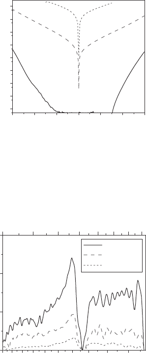
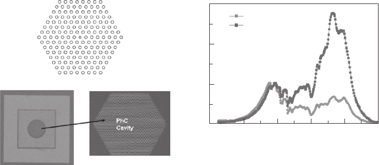
Using photonic crystals as a microcavity resonator, Posani et al. [102] has demonstrated a
signifi cant improvement in the responsivity, conversion effi ciency, and detectivity for a DWELL
detector. A two-dimensional array of holes (PhC) with a 2–3 μ m diameter and a lattice spacing
of 2.4 μ m was fabricated on the DWELL structure using e-beam lithography. A schematic dia-
gram and an image of a hexagonal PhC are shown in Fig. 22.18a and b. PhCs provide a photonic
band gap for normal incidence radiation. By introducing a defect into the crystal, a cavity can
be built, which operates in the wavelength range corresponding to the photonic band gap. The
above parameters were chosen [102] to obtain resonant cavity effects at 8.1 μ m. Two structures,
a DWELL detector and a PhC-DWELL detector [102] , were tested and performance was compared
to determine the effects of PhC. The DWELL detector exhibited two-colour response characteris-
tics with peaks at 6 and 10 μ m. The 6 μ m (dominant at low bias) was due to transitions from the
QD ground state to the continuum, while the 10 μ m peak (dominant at high bias) originated from
transitions from the QD ground state to a bound state in the QW. These electronic transitions and
corresponding response peaks are similar to those of the DWELL detectors reported earlier in this
chapter. An increase in photocurrent by an order of magnitude was reported for PhC-DWELL,
while both DWELL and PhC-DWELL had the same dark current. A comparison of the responsiv-
ity of a PhC-DWELL and a standard DWELL is shown in Fig. 22.18c . At 9 μ m and 78 K under a
2.6 V bias, the PhC-DWELL detector had a conversion effi ciency of 95%, as opposed to the con-
version effi ciency of 7.5% for the DWELL detector. Using conventional optical lithography, PhCs
with 2–3 μ m hole diameter can be easily incorporated into FPA fabrication.
Figure 22.18 (a) Photonic crystal resonant cavity comprising a hexagonal pattern of air holes. (b) Image of a PhC
defi ned in a DWELL detector. (c) A comparison of the spectral responsivity of PhC-DWELL and standard DWELL
detectors at 50 K under a 3 V bias. After [102] .
(a)
(b)
3
2
1
0
2 4 6 8 10 12
Without PC
With PC
Wavelen
g
th (m)
Normalized wrt MWIR
peak
V
b
3 V
Photoresponse (a.u.)
(c)
Similar to PhC-DWELL, an RC-DWELL, in which the active QD region was placed in a Fabry–
Pérot resonant cavity, was reported by Attaluri et al. [78] . This allows radiation to pass multiple
times through the active region within the cavity. The RC was designed to increase the optical
fi eld strength at the peak wavelength of a standard DWELL detector. The RC-DWELL consists of
a regular DWELL (including top and bottom contact layers) grown on a distributed Bragg refl ec-
tor (bottom refl ector), as shown in Fig. 22.19a . The top refl ector was the semiconductor–air
CH022-I046325.indd 678CH022-I046325.indd 678 6/27/2008 3:51:39 PM6/27/2008 3:51:39 PM