Henini M. Handbook of Self Assembled Semiconductor Nanostructures for Novel devices in Photonics and Electronics
Подождите немного. Документ загружается.


Quantum Dot Structures for Multi-band Infrared and
Terahertz Radiation Detection
G. Ariyawansa and A.G.U. Perera
Department of Physics and Astronomy, Georgia State University, Atlanta, GA 30303
22.1 Introduction
In the fi eld of infrared (IR) detector technology, quantum dot infrared photodetectors (QDIPs)
have attracted the attention of researchers aiming to develop IR optoelectronic devices with
improved performance. Compared to quantum well infrared photodetectors (QWIPs), QDIPs have
additional degrees of confi nement, leading to three major advantages [1] : (i) QDIPs are sensitive
to normal-incidence IR radiation, which is forbidden in n -type QWIPs due to polarization selec-
tion rules, (ii) QDIPs exhibit comparatively long effective carrier lifetimes, ⬃ 100s of picoseconds,
which has been confi rmed by both theory [2] and experiment [3] , and (iii) QDIPs exhibit low dark
current. Ideally, QDIPs should show improved performance characteristics such as high respon-
sivity, high detectivity, and high operating temperatures. However, such dramatic improvements
have not yet been demonstrated due to the fact that detection in most QDIPs is based on bound-
to-continuum transitions, as opposed to transitions between the ground state and the fi rst excited
state in the QD.
QDIPs ranging from single-element detectors [4–9] to focal plane arrays (FPAs) [10–12] have
been demonstrated. In addition to the aforementioned advantages, QDIPs show improved radia-
tion hardness [13, 14] and polarization-sensitive spectral responses [15, 16] . QDIPs operating at
temperatures above 77 K [5, 17–22] indicate the possibility of developing uncooled IR imaging
systems. In a recent publication, Matthews et al. [23] reported an extremely long carrier lifetime
of 3–600 ns for a dots-in-a-well (DWELL) detector, which also exhibits a photoconductive gain
of 10
4
–10
5
in the 20–100 K temperature range. In addition to InAs/GaAs (or InGaAs/GaAs)
material system, QDIPs are being developed using SiGe/Si [24–26] and GaN/AlN material sys-
tems [27] . The behaviour of QDs under an applied magnetic fi eld [28, 29] has recently become a
point of interest in order to understand physical mechanisms of QDs as well as future spintronic
devices. The spin of an electron in a QD can be used as a qubit [30–33] for quantum information
processing.
Multi-band IR detection has become an important tool in the fi eld of IR technology due to a
number of applications. Detecting an object’s IR emission at multiple wavelengths can be used
to eliminate background effects and reconstruct the object’s absolute temperature. This also
plays an important role in differentiating the object from its background. Identifi cation of a mis-
sile against its plume is an example. However, measuring multiple wavelength bands typically
requires either multiple detectors or a single broad-band detector coupled to a fi lter wheel in order
to select different wavelength regions of the incident radiation. Both of these techniques are asso-
ciated with complicated detector assemblies, separate cooling systems, electronic components,
CHAPTER 22
CH022-I046325.indd 659CH022-I046325.indd 659 6/27/2008 3:51:30 PM6/27/2008 3:51:30 PM
660 Handbook of Self Assembled Semiconductor Nanostructures for Novel Devices in Photonics and Electronics
and optical elements such as lenses, fi lters, and beam splitters. Consequently, such sensor systems
(or imaging systems) require complex control mechanism hardware to achieve the necessary
fi ne optical alignment. These requirements generally give rise to increased costs, which can be
avoided by a single detector responding in multiple bands. The multi-spectral features are proc-
essed using colour fusion algorithms in order to extract signatures of the object with a maxi-
mum contrast. The development of multi-band detector systems has led to an increased effort by
researchers [34, 35] to develop image fusion techniques. Fay et al. [34] have reported a colour-
fusion technique using a multi-sensor imagery system consisting of four separate detectors,
which operate in different wavelength regions.
There are many applications which will benefi t from multi-band detectors. In landmine detec-
tion [36] , the number of false positives can be reduced using a multi-spectral approach, allowing
the locations of the land-mines to be identifi ed. Military applications include the use of multi-
band detectors to detect muzzle fl ashes, which emit radiation in different wavelength regions
[37] to locate the position of enemy troops and operating vehicles. Multi-band FPAs responding
in very long wavelength infrared (14–30 μ m) can be used for space surveillance and space situ-
ational awareness [38] , where the observation of extremely faint objects against a dark back-
ground is required. Present missile-warning sensors are built specifi cally to detect the ultraviolet
(UV) emission from missile plumes. However, the UV emission from the plume of modern missiles
is low, thus, making UV-based missile detection impractical. As a solution, IR emission [39] from
the plume can be used. The detector system should be able to distinguish the missile plume from
its complex background in order to avoid any possible false alarms. Thus, a single-band detec-
tor would not be suitable. Using a two-colour (or multi-colour) detector, which operates in two
IR bands, which the IR emission of the missile plume falls in, the contrast between the missile
plume and the background can be maximized. Additionally, a multi-band detector can be used
as a remote thermometer [40] , where the object’s emission in two wavelength bands is detected
and the resulting two components of the photocurrent can be solved to extract the object’s
temperature.
The predominant drawback of multi-band detectors is the inability to separate the photocur-
rent components generated by the detection mechanisms without using external optical fi lters.
In order to overcome this, several approaches have been reported. Detector structures with multi-
stack active regions [41] use separate electrical contacts to collect the photocurrent components,
generated in each active region separately. Detectors with bias-selectable response peaks [10,
18] allow the selection of one peak at a time using the applied bias. In this chapter, DWELL and
tunnelling quantum dot infrared photodetector (T-QDIP) structures reported by Ariyawansa
et al. [42] and Bhattacharya et al. [43] , respectively, are discussed in detail. Device design con-
cepts, growth, and detection mechanisms in each of these structures along with theoretical
and experimental results are discussed in sections 22.2 and 22.3. Some of the other multi-band
detectors reported include QWIPs [44–52] , MCT detectors [53–58] , and homojunction- [59,
60] /heterojunction- [61] interfacial workfunction internal photoemission (HIWIP/HEIWIP)
detectors, which are not discussed here as the focus is on multi-band QDIP structures.
22.2 Multi-band quantum dots-in-a-well (DWELL) infrared photodetectors
During the past few years, there has been extensive research in developing DWELL [8, 9, 18, 42,
62, 63, 64, 65] IR detectors. In a typical DWELL structure, InAs QDs are placed in a thin InGaAs
quantum well (QW), which in turn is positioned in a GaAs matrix. The DWELL heterostruc-
ture provides strong confi nement for carriers trapped in the QD by lowering the ground state of
the QD with respect to the GaAs band edge, resulting in low thermionic emission. There can be
one or more confi ned energy states in the QD, with the position and separation of energy states
dependent on the size of the QD as well as the confi nement potential. The detection mechanism
of a DWELL detector involves the transitions of electrons from the QD ground state to an excited
state in either the QD or QW. Energy states associated with the QW can be bound, quasi-bound,
or part of the continuum. These different possible transitions lead to multi-colour character-
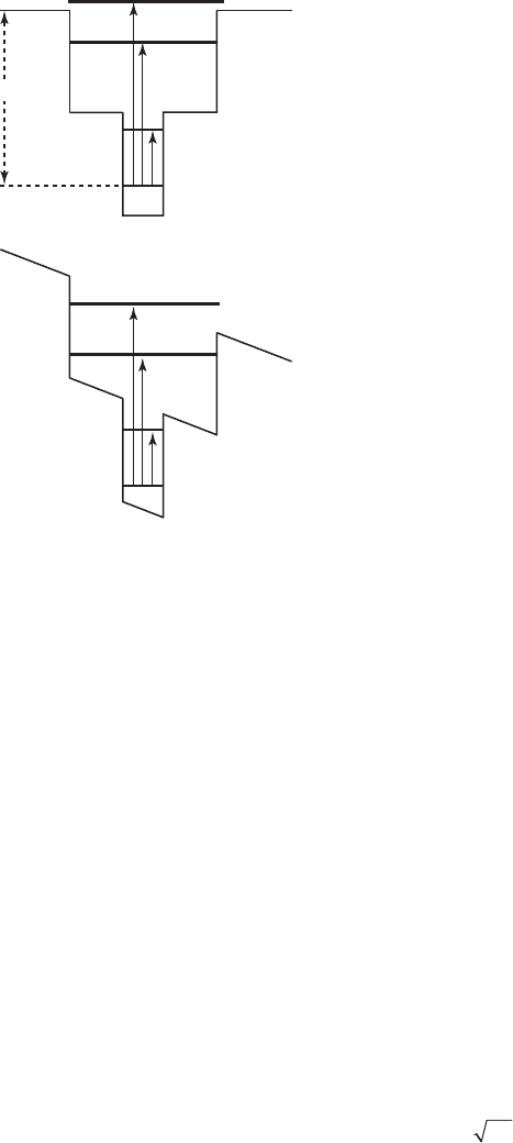
istics. A schematic diagram of the conduction band profi le of a DWELL structure is shown in
CH022-I046325.indd 660CH022-I046325.indd 660 6/27/2008 3:51:31 PM6/27/2008 3:51:31 PM
Quantum Dot Structures for Multi-band Infrared and Terahertz Radiation Detection 661
Fig. 22.1 , along with different transitions between energy states as indicated by the arrows. The
photocurrent, a result of the photoexcitation of carriers, is proportional to the product of the
oscillator strength and the carrier escape probability. A response peak resulting from a bound-
to-bound transition has a stronger oscillator strength and a smaller escape probability than a
response peak resulting from a bound-to-continuum transition. However, the escape probability
can be increased by applying an external electric fi eld. Hence, a bound-to-continuum peak can be
observed even at low biases, whereas a bound-to-bound peak dominates at high applied fi elds due
to enhanced escape probability by fi eld-assisted tunnelling. The energy states in the QD and the
QW can be adjusted independently by changing the parameters associated with each. As a result,
DWELL structures open up a variety of possible designs, leading to multi-band IR detectors.
In this section, three-colour InAs/InGaAs DWELL detectors, with different well widths, are
discussed as previously reported by Ariyawansa et al. [42] . Three DWELL detectors (labelled as
1388, 1373 and 1299) with well widths (120 Å, 110 Å and 90 Å, respectively) were character-
ized. The detectors showed response peaks at three distinct wavelengths in the mid, long, and
very long wavelength/far infrared (MWIR, LWIR, and VLWIR/FIR) regions. The 1388 detector
had peak wavelengths at ⬃ 6.25 μ m, ⬃ 10.5 μ m and ⬃ 23.3 μ m. All observed peaks correspond to
the energy difference of intersubband transitions in the DWELL heterostructure. The two peaks
at 6.25 μ m and 10.5 μ m are a result of bound-to-bound transitions from the ground state in the
QD to a state in the QW, whereas the longer wavelength peak ( ⬃ 23.3 μ m) is due to an intersub-
band transition between QD levels. The 23.3 μ m peak has a detectivity of 7.9 1 0
10
c m
Hz/W
at 4.6 K under a 2.2 V bias. Spectral response in the 1388 detector has been observed up to
80 K. The operating wavelength of these detectors in the MWIR and LWIR regions can be tai-
lored by changing the width of the QW. When the width of the QW is increased, the two peaks in
the MWIR and LWIR regions show a red shift, while the VLWIR peak remains around ⬃ 2 3 . 3 μ m.
This observation confi rms that the LWIR peaks are associated with dot-to-well transitions and
the VLWIR peak originates from transitions between energy states within the well.
GaAs
barrier
GaAs
barrier
GaAs
barrier
GaAs
barrier
248 meV
InGaAs
well
InGaAs
well
InGaAs
well
InGaAs
well
InAs QD
InAs QD
(a)
(b)
Figure 22.1 Conduction band profi le of a DWELL structure (a) under zero bias and (b) under a negative bias. The
energy states corresponding to possible transitions leading to spectral response peaks are indicated by arrows.
CH022-I046325.indd 661CH022-I046325.indd 661 6/27/2008 3:51:31 PM6/27/2008 3:51:31 PM
662 Handbook of Self Assembled Semiconductor Nanostructures for Novel Devices in Photonics and Electronics
22.2.1 DWELL device structure
The DWELL detector structures reported by Ariyawansa et al. [42] (1388, 1373, and 1299) were
grown [66] in a VG-80 solid source molecular beam epitaxy (MBE) system with a cracked As
2
source at the University of New Mexico. The GaAs layers were grown at a substrate temperature
T
sub
580°C, whereas the In
0.15
Ga
0.85
As QW and the InAs QDs were grown at T
sub
480°C. The
temperature was measured using an optical pyrometer. Using standard lithography, metal evapo-
ration and wet etching techniques, n-i-n detector mesas were fabricated for top-side illumination.
Mesas with various circular optically active areas (diameters ranging from 25 to 300 μ m) were
fabricated to test for leakage current and uniformity of structures. A more detailed discussion on
the growth process can be found in [66] .
GaAs (n = 1 2 10
18
cm
3
) 0.2 μm
GaAs 500 Å
In
x
Ga
1x
As 60 Å x 0.15
n-doped InAs QDs 2.2ML
In
x
Ga
1x
As 60 Å x 0.15
GaAs (n 1 2 10
18
cm
3
) 0.5 μm
GaAs SI Substrate
(n 1 2 10
18
cm
3
) 500 μm
X10
w
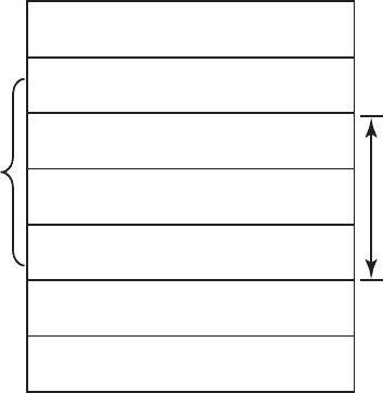
Figure 22.2 A schematic diagram of a DWELL structure. The width of the QW, i.e. the combined thickness of
In
0.15
Ga
0.85
As layers (indicated as w in the fi gure), is different for each detector. Structures 1299, 1373 and 1388
have well widths of 90, 110, and 120 Å, respectively, while all other parameters are the same. After [42] .
The structure of the 1388 detector is shown in Fig. 22.2 . The QDs were doped n -type with
silicon to a sheet density of 5 1 0
11
cm
2
, which corresponds to about one electron per QD.
The QW was not intentionally doped. It has been found [65] that the optimal doping concen-
tration for DWELL detectors corresponds to about one electron per QD. The size of the QDs is a
critical parameter in the detector design and is controlled by growth conditions, especially the
temperature and growth rate. Any inhomogeneous QD size fl uctuation will lead to a broaden-
ing of spectral response peaks. There is a 2D distribution of QDs on a plane perpendicular to the
growth direction; the formation of QDs above another QD is not possible since there is no barrier
to separate the two QD layers. The width of the QW, i.e. the combined thickness of In
0.15
Ga
0.85
As
layers, is denoted by ω . The other two detectors (1373 and 1299) are identical to the 1388 sam-
ple except for the width of the QW. In 1373 and 1299 detector structures, the thickness of the
bottom In
0.15
Ga
0.85
As layer is 50 Å and 30 Å, respectively, while the top In
0.15
Ga
0.85
As layer
thickness is the same (60 Å) for both structures; thus, providing a 110 and 90 Å well width,
respectively. There are ten periods of In
0.15
Ga
0.85
As/ n -InAs/In
0.15
Ga
0.85
As regions in each
of the three detector structures. Square mesa devices with 400 4 0 0 μ m dimensions were
processed, and a 300 μ m diameter opening was left in the top contact for front-side illumina-
tion. Photoluminescence measurements of the ground-state transition of the QD (1.25 μ m at
T 300 K) with a 60:40 conduction to valence band ratio, were used to estimate the ground
state of the QD, which is approximately 250 meV below the GaAs band edge. There can be at least
two bound states in the QD and one confi ned state in the QW [9] , as shown in Fig. 22.1 . Possible
carrier transitions, leading to the spectral response peaks, are indicated by arrows.
CH022-I046325.indd 662CH022-I046325.indd 662 6/27/2008 3:51:31 PM6/27/2008 3:51:31 PM

Quantum Dot Structures for Multi-band Infrared and Terahertz Radiation Detection 663
An energy level calculation model for a DWELL system was proposed by Amtout et al. [62] .
DWELL structures with different QDs have been tested experimentally, and electronic spectra
obtained by the model are in good agreement with the experimental results. The shape of the
QDs is pyramidal as confi rmed by transmission electron microscopy. The Hamiltonian of a system
with a quasi-zero-dimensional QD placed in a two-dimensional QW is defi ned with a potential
energy consisting of four terms: the potential in the QD region, the potential in the QW region,
the potential in the barrier region, and the potential from the applied electric fi eld. The eigen-
functions of the Hamiltonian are derived using a Bessel function expansion. The DWELL detec-
tors tested by Amtout have QDs with base dimensions of 110 and 140 Å and heights of 65 and
50 Å, respectively. The energy spacing between the fi rst and second energy levels obtained from
the model for the two samples are 132 and 150 meV, whereas experimental analysis showed
energy spacing of 123 and 140 meV, respectively. Although the energy states are shifted by the
electrostatic potential from the bias fi eld, the energy spacing between the fi rst two energy states
was not changed by the applied electric fi eld. This can be observed in the spectral response of
many DWELL detectors.
22.2.2 Device characterization techniques
The spectral response of the device under test and an Si composite bolometer with a known sen-
sitivity were measured with a Fourier transform infrared (FTIR) spectrometer. The two spectra
were obtained concurrently and used the same combination of optical windows, beam splitter
and fi lters, so that the optical path was identical. The device spectrum ( I
d
) was divided by the
bolometer spectrum ( I
b
) and then multiplied by the bolometer sensitivity (S
0
) in order to obtain
the voltage responsivity of the device:
RV W
GS I
I
d
b
() ./
0
(22.1)
here G is a geometrical factor which corrects for differences in the radiation incident area of
the detector and the bolometer. To obtain the current responsivity, the voltage responsivity was
divided by the effective resistance. Since the detector and load resistor act as a voltage divider for
the photocurrent, the effective resistance R
e
is the parallel combination of the load R
l
and the
detector dynamic resistance R
d
dV / dI , yielding R
e
R
l
R
d
/( R
l
R
d
). The fi nal current respon-
sivity is given by
RAW
GS I R R
IRR
dl d
bld
()
()
()
./
0
(22.2)
The specifi c detectivity ( D *) of the devices at different temperatures and applied biases was
obtained from the measured peak responsivity ( R
p
), noise current density ( S
i
), and the illumi-
nated area of the detector ( A ). The noise current density was measured with a dual channel fast
Fourier transform (FFT) signal analyser and a low-noise preamplifi er. A thick copper plate, which
is at the device temperature, was used to block radiation, thus providing the dark conditions nec-
essary for the measurements. The value of D * is calculated from:
D
RA
S
p
i
*
()Jones
/
/
12
12
(22.3)
with
Sif
in
2
/Δ
, i
n
is the noise current, and Δ f is the noise bandwidth.
The quantum effi ciency is given by:
η
λ
hcR
gq
p
(22.4)
CH022-I046325.indd 663CH022-I046325.indd 663 6/27/2008 3:51:32 PM6/27/2008 3:51:32 PM
664 Handbook of Self Assembled Semiconductor Nanostructures for Novel Devices in Photonics and Electronics
where h is the Planck constant, c is the speed of light, g is the photoconductive gain, q is the elec-
tron charge, and λ is the wavelength.
The photoconductive gain ( g ) can be defi ned as the ratio of the total collected carriers to the
total excited carriers generated by both thermal and photoexcitations. Assuming carrier emis-
sion and capture are due to generation–recombination ( g – r ) processes, g can be derived experi-
mentally from [5] :
g
S
qI N
i
d
4
1
2
(22.5)
where I
d
is the measured dark current and N is the number of QD layers.
22.2.3 Experimental results and effects of the well width on response peaks
In order to explain the transition between energy states leading to response peaks, the experi-
mental results of the three DWELL detectors reported by Ariyawansa et al. [42] will be discussed.
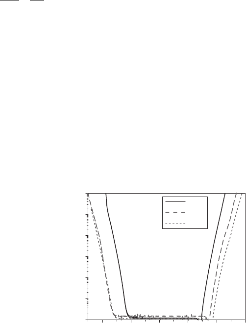
A comparison of dark current–voltage ( I – V ) characteristics for all three structures is shown in
Fig. 22.3 . The sample 1388 showed the lowest dark current, and it increased when the width
of the QW was increased. All three detectors exhibited three distinct peaks (three colours) in the
MWIR, LWIR, and VLWIR regions (labelled as fi rst, second, and third peak, respectively). The
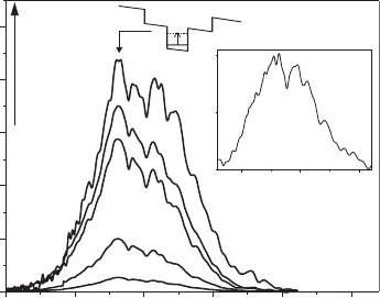
results for the 1388 detector under different bias voltages are shown in Fig. 22.4 . The band dia-
gram, with corresponding transitions indicated by arrows, is shown in the inset to Fig. 22.4 . The
origin of each peak will be explained in detail in the following sections.
10
4
10
6
10
8
10
10
2
1
0
1
2
3
Bias voltage (V)
T 4.6 K
1299
1373
1388
Dark current (A)
Figure 22.3 A comparison of dark I–V characteristics of three DWELL structures (1299, 1373, and 1388)
at 4.6 K. The mesas tested have the same electrical area. The sample 1388 showed the lowest dark current, and a
decrease of dark current is observed as the width of the QW increases. Modifi ed after [42] .
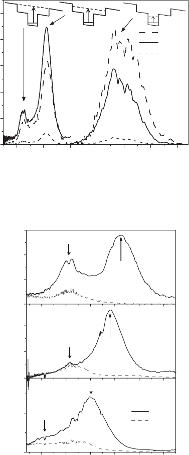
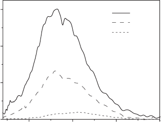
The spectral response of the three detectors in the MWIR/LWIR regions for 0.5 V and
1.4 V bias voltages is shown in Fig. 22.5 . All three detectors showed two distinct peaks in
this wavelength range. The 1299 detector exhibited the fi rst peak at ⬃ 4 . 2 μ m and the second
peak at ⬃ 8 . 1 μ m. A semi-empirical estimate based on the photoluminescence spectra with a
60:40 split of the band gap difference gives a 225–250 meV ( ⬃ 4.9 – 5.5 μ m) energy separation
between the ground state of the QD and the conduction band edge of GaAs. Hence, the 4.2 μ m
peak is probably due to transitions from the ground state of the QD to the continuum state of the
QW, and the second peak is due to transitions from the ground state of the QD to a bound state
in the QW, as shown in Fig. 22.1 . Moreover, it has been shown [67] that the line width ( Δ λ / λ ) of
a peak due to transitions from bound-to-bound states is narrower than that of transitions from
CH022-I046325.indd 664CH022-I046325.indd 664 6/27/2008 3:51:32 PM6/27/2008 3:51:32 PM
Quantum Dot Structures for Multi-band Infrared and Terahertz Radiation Detection 665
2.40 V
2.20 V
2.00 V
5 101520253035
0
1
2
3
4
5
5
Responsivity (A/W)
Wavelength (μm)
Figure 22.4 Three-colour response of 1388 detector under different bias voltages at 4.6 K. The band diagram with
the corresponding transitions indicated by arrows are shown in the inset.
3
0
2
10
0
10
0
5
1
4.2 μm
9.7 μm
6.25 μm
8.1 μm
46810 1412
Wavelength (μm)
1.4 V
0.5 V
T 4.6 K
1373
1388
1299
6.25 μm
10.5 μm
4
5
Responsivity (mA/W)
Figure 22.5 The fi rst two peaks of the three detectors biased with 1.4 V and 0.5 V at 4.6 K. Arrows indi-
cate the peak positions and the sign implies that the curve has been multiplied by the specifi ed number. Modifi ed
after [42] .
bound-to-continuum states. The linewidth of the 4.2 μ m peak is approximately 42%, whereas
the linewidth of the 8.1 μ m peak is approximately 28%; this observation is consistent with the
aforementioned description. The escape probability of carriers excited to a bound state increases
with increasing bias due to fi eld-assisted tunnelling. Thus, the bound-to-bound peak (at 8.1 μ m)
shows a stronger dependency on the applied bias than the bound-to-continuum peak (at 4.2 μ m),
as evident from Fig. 22.5 .
CH022-I046325.indd 665CH022-I046325.indd 665 6/27/2008 3:51:32 PM6/27/2008 3:51:32 PM
666 Handbook of Self Assembled Semiconductor Nanostructures for Novel Devices in Photonics and Electronics
When the width of the QW is increased the energy spacing between the states in the QW
decreases. At the same time, the energy spacing between QD ground state and states in QW also
decreases. Thus, a red shift of the fi rst and second peaks is observed. The results for the 1299 and
1388 detectors confi rm this notion. In addition, the 1388 detector exhibits a quasi-bound state
close to the band edge of the GaAs barrier, and hence the fi rst peak of the 1388 detector is due to
transitions from the ground state of the QD to the quasi-bound state in the QW. This can be con-
fi rmed by the red shift and the reduced linewidth for the fi rst peak of the 1388 detector as compared
to the fi rst peak of the 1299 detector. Based on width of the QW in detector 1373, its peaks are
expected to be located in between the peaks of the 1299 and 1388 detectors. However, the experi-
ment showed a longer red shift than expected in both fi rst and second peaks of the 1373 detec-
tor with respect to the 1299 detector. This discrepancy in the result for the 1373 detector could be
explained by an unintentional change in the QD size during the growth process. Further discussion
on this will be given in following sections. Moreover, several unexplained features in the responsiv-
ity spectra, such as line splitting, were also observed. Based on doping concentration and sheet den-
sity of QDs, it has been found [8] that a single QD consists of one electron. Multiple electrons within
a QD could lead to a splitting of photoresponse peaks due to intralevel and interlevel Coulomb inter-
actions [68] . Therefore, the secondary peaks superimposed on the primary peaks may result from
either different QD sizes in the same DWELL structure or Coulomb interactions between multiple
electrons in the QD. The expected red shift due to Coulomb interaction with an applied electric fi eld
could be compensated by the blue shift due to the Stark effect [68] . Splitting of absorption peaks is
also possible through interdot coupling [69] , which depends on the random distribution of QDs.
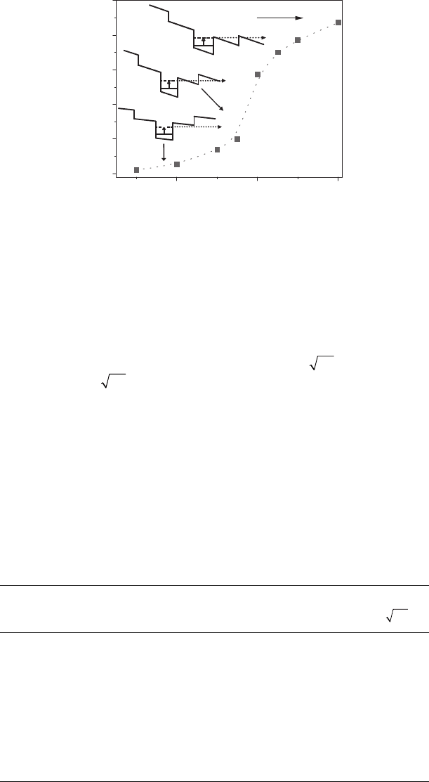
The spectral responsivity of the third peak of the 1388 detector in the VLWIR region, under
different applied electric fi elds, is shown in Fig. 22.6 . For QDs with a base diameter of 20 nm and
a height of 7–8 nm, the energy separation between the ground and fi rst excited state calculated
from 8-band k p model [70] , is about 50–60 meV. Thus, it is believed that the VLWIR peak at
⬃ 2 3 . 3 μ m is due to transitions between two bound states within the QD. The energy level dia-
gram corresponding to this transition is shown in the inset to Fig. 22.6 . The variation of the peak
responsivity of the 23.3 μ m peak with applied bias is shown in Fig. 22.7 . As shown in the energy
band diagrams in the inset to Fig. 22.7 , carriers excited from the ground state to the fi rst excited
state in the QD have to tunnel through the barrier into the continuum, in order to be collected
by the external circuit. With increased fi eld strength, the barrier is pulled down strongly, allow-
ing the excited carriers to tunnel through a thinner barrier. This leads to fi eld-assisted tunnel-
ling, where the applied fi eld increases the escape probability of excited carriers. As a result, the
experimental response curves showed a drastic increase in response when the reverse bias was
increased from 1.0 V to 2.4 V. Moreover, the peak at 23.3 μ m was broader than that would be
expected for a bound-to-bound transition in the QD. This is attributed to an ⬃ 10% size fl uctua-
tion of the QDs during the self-assemble growth process.
15 20 25 30 35 40
Wavelength (μm)
5
4
1
3
2
0
Responsivity (A/W)
2.40 V
2.00 V
2.25 V
2.15 V
2.20 V
T 4.6 K
20
25
30
Wavelength (μm)
T 79 K
Responsivity (a.u)
Figure 22.6 The VLWIR response of 1388 at different bias values (negative indicates that the top contact is negative).
The band diagram represents the transition leading to the response. The inset shows the responsivity at 79 K. After [42] .
CH022-I046325.indd 666CH022-I046325.indd 666 6/27/2008 3:51:33 PM6/27/2008 3:51:33 PM
Quantum Dot Structures for Multi-band Infrared and Terahertz Radiation Detection 667
Device parameters and the fi gures of merit for the three detectors (1299, 1373, and 1388)
under the optimum operating conditions are given in Table 22.1 . The VLWIR peak of the 1373
detector could be obtained up to 60 K, while the VLWIR peaks of the 1299 and 1388 detectors
were observed up to 80 K. The highest observed detectivity for the 1388 detector at 23.3 μ m
under a 2.2 V bias at 4.6 K was reported as ⬃ 7.9 1 0
10
c m
Hz/W
. At 80 K a maximum
detectivity of 3.2 1 0
8
c m
Hz/W
was reported under a 1.4 V bias for the 1388 detector. At
23.3 μ m, the 1388 detector exhibited lower responsivity and a lower noise current than those
of the 1299 detector (a comparison of dark current is given in Fig. 22.3 ), resulting in a higher
detectivity for the 1388 detector than for the 1299 detector. The improvement in operating tem-
perature of the VLWIR response (up to 80 K), compared with a typical VLWIR QWIP [71] operat-
ing at ⬃ 10–20 K, demonstrates the benefi t of a quasi-zero dimensional confi nement.
Table 22.1 Responsivity and detectivity of the three response bands of
1299, 1373, and 1388 DWELL detectors reported by Ariyawansa et al. [42] at
4.6 K with 1.4 V bias (⬃ 22.5 kVcm
1
fi eld). All three structures have InAs
QDs placed in an InGaAs/GaAs QW. The QDs were doped n-type with silicon
to a sheet density of 5 1 0
11
c m
2
. The QDs in all three structures were
grown to the same in size. After Reference [42] .
Sample number Well width (Å)
λ
peak
( μ m)
Responsivity
(mA/W)
Detectivity
(cm
Hz/W
)
1299 90 4.2 3.9
1.1 1 0
9
8.1 14.0
3.9 1 0
9
23.3 60.2
1.9 1 0
10
1373 110 6.25 3.0
5.4 1 0
9
9.7 12.9
2.3 1 0
10
25.5 3.8
6.9 1 0
9
1388 120 6.25 1.8
6.2 1 0
9
10.5 2.8
1.7 1 0
10
23.3 25.6
6.6 1 0
10
2.0 2.2 2.4
0
1
2
3
4
5
T = 4.6 K
Peak responsivity (A/W)
Bias voltage (V)
Figure 22.7 Variation of the peak responsivity of the 1388 detector with applied bias. Variation of the conduction
band profi le with applied bias (electric fi eld) shows that excited electrons escape through the barrier by fi eld-assistant
tunnelling. After [42] .
As shown in Fig. 22.8 , the VLWIR peak of both the 1299 and 1388 detectors occurs at
approximately the same wavelength (23.3 μ m). Changing the width of the QW does not affect
the energy states in the QD, thus confi rming that the VLWIR peak is due to transitions between
CH022-I046325.indd 667CH022-I046325.indd 667 6/27/2008 3:51:33 PM6/27/2008 3:51:33 PM
668 Handbook of Self Assembled Semiconductor Nanostructures for Novel Devices in Photonics and Electronics
QD states. However, the VLWIR peak of the 1373 detector appeared at 25.5 μ m, as shown in Fig.
22.8 , and red shifted with respect to the VLWIR peaks of the 1299 and 1388 detectors. This
observation was attributed to the unintentional increase of QD size in the 1373 detector during
the growth process, resulting in a decreased energy spacing between the ground and the fi rst
excited states in the QD. In addition, this would also decrease the energy spacing between the
ground state in the QD and the bound state in the QW. As a result, the fi rst two peaks will appear
at longer wavelengths than expected. This shift was observed in the spectral response curves of
the 1373 detector (see Fig. 22.5 ).
22.3 Tunnelling quantum dot infrared photodetectors (T-QDIPs)
At present, commercially available IR detectors only work at cryogenic temperatures, thus single-
element devices and FPAs made of these detectors require cryogenic coolers and assemblies. These
detector systems are not only complicated and bulky, but also very expensive. The most effective
way to overcome these drawbacks would be the development of IR detectors capable of operating
at room temperature. However, the development of room temperature IR detectors is a challenge
as the rate of thermal excitations leading to the dark current increases exponentially with tempera-
ture. While a QD-based structure is a potential choice, conventional QDIP structures have not yet
shown adequate performance above 150 K. At temperatures above 150 K electron occupation is
dominated by the excited states in the QD; and, as a result, the reduction in the dark current is not
signifi cant. As a solution, Bhattacharya et al. [43] have explored a new resonant tunnel-based QD
device architecture, demonstrating room temperature IR detection at 6 and 17 μ m.
Aslan et al. [72] have recently observed resonant tunnelling through a QD layer. In general,
any device structure designed to reduce the dark current will also reduce the photocurrent.
Recently reported T-QDIPs [43, 70, 73, 74, 75] used resonant tunnelling to selectively collect
the photocurrent generated within the QDs, while the tunnelling barriers (double-barrier
system) block the majority of carriers contributing to the dark current. The maximum operat-
ing temperature of detectors is associated with the dark current, which in turn related to the
detector response wavelength region. Ideally, the resonant tunnelling approach can be used
to develop IR detectors operating at high temperatures irrespective of the response wave-
length region. The characteristics of the room temperature T-QDIP reported by Bhattacharya
et al. , showing two-colour response at wavelengths of ⬃ 6 and ⬃ 1 7 μ m are discussed in this
section.
A T-QDIP structure can be considered as an extended DWELL structure. That is, a DWELL struc-
ture coupled with a double-barrier system transforms into a T-QDIP structure, which has several
advantages over DWELL structures. Conventional QDIPs have inherently low dark current, which
60
0
20
20 353025
40
Wavelength (m)
Responsivity (mA/W)
w 90
110
120
1373
1299
1388
Figure 22.8 Spectral response of the VLWIR peak for all three detectors at 4.6 K under a 1.4 V bias ( 23.7,
22.9, and 22.5 kVcm
1
fi eld for 1299, 1373, and 1388, respectively). After [42] .
CH022-I046325.indd 668CH022-I046325.indd 668 6/27/2008 3:51:34 PM6/27/2008 3:51:34 PM