Henini M. Handbook of Self Assembled Semiconductor Nanostructures for Novel devices in Photonics and Electronics
Подождите немного. Документ загружается.

Optically Driven Schemes for Quantum Computation Based on Self-assembled Quantum Dots 689
This overall prescription is straightforward, but there are several considerations to be made
when designing a quantum computer. We highlight three here, as follows:
● Decoherence . Nature does not provide perfectly isolated two-level systems. The real sys-
tems interact in a non-predictable way with the surrounding environment and its fl uctua-
tions. In solid-state hardware these may constitute, for example, the crystal phonon modes
or the presence of spurious charges. Additionally the qubit is often physically embodied in
two of the many levels of a quantum system. Unwanted transitions to the additional lev-
els may happen. All of this spoils the quantum computation, by arbitrarily modifying the
state of the systems on which the quantum gates are performed. In fact, the situation is
often even worse than this: the environment entangles itself with the quantum computer
in such a way as to destroy its quantum coherence and the unitarity of its quantum evolu-
tion. This phenomenon is known as decoherence and it underpins the inherent fragility of
quantum computation, when thought of as a sequence of controlled quantum evolutions
of an ensemble of selected quantum levels.
● Scalability . To perform non-trivial calculations, a quantum computer should contain a
minimum number of qubits. When considering quantum algorithms that provide an
exponential speed-up over classical counterparts [6] , the actual number can be as small as
a few tens of qubits. However, building, addressing and controlling the quantum dynam-
ics of several two-level quantum systems is very challenging. The possibility of doing so
strongly depends on the chosen hardware, qubit encoding or gating scheme.
● Error correction . As for classical computers, it is important to be able to detect and correct
errors during the computation itself. Various schemes have been proposed to achieve this
[1] , and usually each scheme detects and corrects specifi c classes of errors. One of the main
diffi culties in designing error correction codes for quantum computation is that the collapse
of the wave-function following measurement destroys the quantum information stored. This
implies that it is not possible to resort to straightforward classical codes to detect (and correct)
faulty computation. In general, error correction codes require redundant information to be
encoded and propagated during the computation. This translates into an increased demand
of resources, such as number of qubits and number and type of gates to be performed.
Since there are many criteria that must be satisfi ed by a quantum computer, a lot of differ-
ent physical implementations have been proposed, each with its own advantages and problems.
No fundamental physical obstacles exist, but from the technological point of view, building a
quantum computer is extremely demanding. Some example forerunner qubit embodiments are
the polarization of single photons, nuclear spins in organic molecules, phosphorus impurities in
silicon, charge carriers in superconductors and hyperfi ne levels of ions trapped by electromag-
netic fi elds [1] . A very promising possibility is solid-state implementations, especially schemes
based on semiconductor devices. Such approaches allow for the exploitation of techniques
already developed for producing micro- and nanostructures, and of the detailed work that has
already been done on their electronic properties. Using sophisticated optoelectronics methods,
it has also been demonstrated that excitations in semiconductors can be generated and their
dynamics driven using ultra-fast laser pulses. As we will see, this allows accurate generation and
control of quantum states that can be used for quantum computation. Moreover, these dynam-
ics can be driven on sub-picosecond timescales, which are much faster than the related decoher-
ence times. Finally, the use of semiconductor-based hardware should facilitate the connection
of quantum registers and processors to traditional electronics circuits, which is certain to be an
essential component of any complete device.
23.2 Semiconductor self-assembled quantum dots as hardware
In this chapter we will discuss designs which use semiconductor self-assembled QDs as hardware
in some detail [7] . QDs can form when two (or more) types of semiconductor form a heterostruc-
ture. As an example, consider a GaAs/InAs structure grown by molecular beam epitaxy (MBE).
CH023-I046325.indd 689CH023-I046325.indd 689 6/27/2008 6:36:28 PM6/27/2008 6:36:28 PM
690 Handbook of Self Assembled Semiconductor Nanostructures for Novel Devices in Photonics and Electronics
In the fi rst stage of processing, Ga and As atoms are evaporated slowly on to a GaAs substrate
such that a perfectly fl at surface results. Second, Ga is replaced by In in the growth process, so
that InAs grows instead of the larger band gapped GaAs. Since the lattice constant of these two
materials is different, the InAs layers clump together into small three-dimensional structures
that minimize the combined energy of the surface, volume and strain in the structure. This small
structure, which is typically 10–50 nm in the in-plane direction, and 2–10 nm high, forms the
quantum dot. Subsequent capping by more GaAs ensures electron and hole confi nement in all
three dimensions. Figure 23.2 is a schematic drawing comparing the bulk energy level struc-
ture of a direct gap semiconductor with that of the same semiconductor in quantum dot form.
Confi nement leads to discretization of both electron and hole states – and for this reason QDs are
sometimes called “ artifi cial atoms ” [7] . If another layer of InAs is grown after capping with GaAs,
more QDs form. These lie preferentially above the fi rst layer due to the effect of strain propagation
through the capping layer, such that quantum dot molecules formed by stacked QDs can be made
with a controlled spacing between the constituents [8] . It is also important to emphasize that the
spin quantum numbers of each carrier type are preserved from the bulk structure (see Fig. 23.2 ).
ωω
k
x
Electrons
Heavy holes J 3/2, J
z
/3/2
Light holes
J 3/2, J
z
/1/2
J 1/2, J
z
/1/2
Split off holes
J 1/2 J
z
/1/2
e2
e1
hh1
hh2
lh1
V(x)
(a) (b)
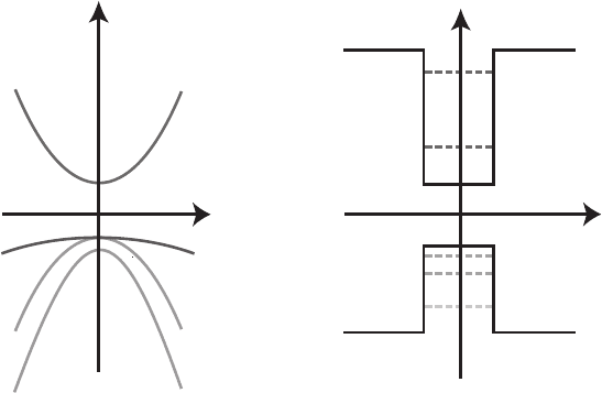
Figure 23.2 (a) Dispersion relation for a typical, direct gap, bulk semiconductor. ω is the energy and k the
wavevector close to the centre of the Brillouin zone. Only the bands closest to the Fermi level are shown. (b) When a
confi ning potential is applied, the bands split into discrete energy levels, but the spin quantum numbers are preserved.
“ hh ” denotes heavy hole, “ lh ” light hole, and “ e ” electron.
Recent experimental developments have shown excellent control over the density, size, shape
and position of QDs. Regular two- and three-dimensional arrays have been fabricated [9–11] (see,
e.g., Fig. 23.1 ), as well as homogeneous in-plane QD chains [12] . With the use of laser pulses of
specifi c length and frequency, selected interband transitions can be addressed and confi ned exci-
tons can be controlled coherently [13–20] . Moreover, by altering the dimensions and shape of a
QD, it is possible to engineer its electronic structure, and hence tune its excitation spectrum. The
optical activity of QDs and photons make them ideal candidates for hybrid schemes in which the
computation is carried out using solid-state qubits (e.g. excitons or electronic spins), while long
distance communication between different processors in the computer or different computers
can be carried out by transferring the quantum information to photons. All of these properties
make QD-based structures very promising candidate quantum computers.
The following are the most obvious possible qubit embodiments in QDs:
● T h e presence or absence of an exciton (or bound state of an electron and hole).
● T h e spin of an exciton.
CH023-I046325.indd 690CH023-I046325.indd 690 6/27/2008 6:36:29 PM6/27/2008 6:36:29 PM
Optically Driven Schemes for Quantum Computation Based on Self-assembled Quantum Dots 691
● T h e spin of an excess electron, added to the conduction band by doping, gating or similar
means.
● T h e spin of an excess hole, added to the valence band by doping, gating or similar means.
The fi rst and third items on this list are substantially more popular choices than the others, so
we shall focus here on these two. Though there are several unifying features of the two represen-
tations, it turns out that the details of how to build a quantum computer using each have quite
distinct features. We will therefore discuss each individually.
23.3 Exciton representation
23.3.1 Single-qubit manipulation
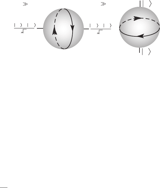
Consider fi rst a single quantum dot representing a single qubit. In order to manipulate this qubit,
we use a pulsed laser. The state of a single qubit can be represented on the surface of a sphere
(the “ Bloch sphere ” ), with the poles of the sphere representing the
0
and
1
, and the azimuthal
angle representing the relative phase of these basis states [1] . Rotations on the Bloch sphere can
be performed using a laser that is resonant with the exciton creation energy in the dot – and by
varying the amplitude, phase and duration of a laser pulse an arbitrary single-qubit gate can be
executed.
We can see this rather easily. Consider the Hamiltonian of an exciton qubit interacting with an
oscillating fi eld in the spin representation:
Hε σσ ωφ
zx l
it HcΩ {[( )] ..}.exp
(23.1)
The σ
x
and σ
z
are the Pauli matrices, ε is the energy of the optical gap (including the exciton
binding energy), Ω is the exciton–laser coupling (also known as the Rabi frequency), and ω
l
is the
laser frequency (which for resonance is set to ε ) .
We now make two transformations. First, we recast the Hamiltonian in a frame rotating with
the laser frequency (this is an exact transformation); second, we ignore fast oscillating expo-
nential terms (this is the rotating wave approximation or RWA). This yields a time independent
Hamiltonian:
H νσ φσ φσ
zxy
Ω(cos( ) sin( ) )
(23.2)
with ν ε ω
l
the detuning of the laser from resonance. Setting ν 0 causes the eigenstates
of the Hamiltonian to lie in the equatorial plane of the Bloch sphere depicted in Fig. 23.3 , with
the azimuthal angle of the two diametrically opposite eigenstates being φ . Since the natural
evolution of the system is to rotate around the line connecting the two eigenstates on the Bloch
sphere, any general single-qubit rotation can be achieved by varying φ and the duration of the
laser pulse.
1
0
0
1
2
0
1
2
XZ
Figure 23.3 Single-qubit rotations on the Bloch sphere. Left : The eigenstates are
(| | ) /012〉〉
, so the state
precesses around the x -axis. Right : The eigenstates are |0 and |1 so the state precesses around the z -axis. In order
to effect an arbitrary single-qubit gate, two rotation axes are needed, together with control of the time of rotation.
CH023-I046325.indd 691CH023-I046325.indd 691 6/27/2008 6:36:29 PM6/27/2008 6:36:29 PM
692 Handbook of Self Assembled Semiconductor Nanostructures for Novel Devices in Photonics and Electronics
23.3.2 Two-qubit manipulation
In order to achieve entanglement between a pair of exciton qubits, there must exist some kind
of controllable interaction between them. Two principal types of natural interaction have been
proposed in this context: the biexcitonic shift and Foerster energy transfer. Each of these will now be
described, and control procedures will be introduced.
23.3.2.1 Biexcitonic shift
For the schemes we are considering, we are interested in exciting at most one exciton in each QD.
In particular, we will consider heavy-hole to conduction band ground state transitions in III–V
semiconductor nanostructures, and drive them by resonant circularly polarized laser pulses. In
this way the spin of the exciton is well defi ned and in particular each laser pulse can couple to
one and only one ground state exciton in each quantum dot. Owing to the Coulomb interaction,
two excitons in nearby QDs may couple and the signature of this coupling is the so-called biexci-
tonic shift [22, 23] . In the following we will consider two vertically stacked QDs, QD
a
and QD
b
(see
Fig. 23.4 ). The biexcitonic shift Δ ε is between the optical response corresponding to the ground-
state excitonic transition in QD
b
in the presence of an exciton in QD
a
compared with the same
h
a
h
a
h
b
h
b
z (nm)
b
ba
Valence band
a
Potential profile
a
a
b
b
Conduction
band
e
b
e
a
e
a
e
b
x (nm)
z (nm)
Field
direction
(b)(a)
GaN/AlNGaAs/AlAs
8100246
10
8
4
10
0
4
8
0
20
Figure 23.4 Electron and hole particle distributions for the biexcitonic ground state in coupled GaAs/AlAs (a) and
GaN/AlN (b) QD structures [28] . The distributions are calculated from direct diagonalization of the many-body
Hamiltonian. The corresponding valence and conduction bands are also sketched.
transition in QD
b
with no exciton in neighbouring QD
a
. Δ ε is dipole–dipole to lowest non-zero
order in the dot centre–centre separation R , so takes the form:
||Δε ∝
d
R
2
3
(23.3)
with d the length of the excitonic electron–hole dipole. If we consider a stack of QDs with a
typical distance between QD centres of 100 Å, interactions beyond nearest neighbours can be
neglected. We will consider structures in which single particle tunnelling between QDs is sup-
pressed [21] , so that the biexcitonic shift stems from direct Coulomb interaction.
We will concentrate here on two different heterostructures, GaAs/AlAs [22, 23] (with GaAs-
based QDs) and GaN/AlN [24, 25] (with GaN-based QDs). These two structures have very different
CH023-I046325.indd 692CH023-I046325.indd 692 6/27/2008 6:36:30 PM6/27/2008 6:36:30 PM

Optically Driven Schemes for Quantum Computation Based on Self-assembled Quantum Dots 693
characteristics. GaAs/AlAs has a zinc-blende structure characterized by a face-centred cubic cell.
This structure presents no spontaneous crystal polarization, and the natural dipole associated
with a ground-state exciton is very small, so that the corresponding biexcitonic shift would be too
small to be resolved by sub-picosecond laser pulses. In order to increase this interaction a static,
in-plane electric fi eld E may be applied [22, 23] . An estimate of the corresponding dipole length
is given by:
deE
mm
ee hh
11
22
ωω
⎛
⎝
⎜
⎜
⎜
⎜
⎞
⎠
⎟
⎟
⎟
⎟
(23.4)
where m
e
(
h
)
is the electronic (hole) mass and ω
e
(
h
)
is the characteristic frequency of the electronic
(hole) in-plane confi ning potential (assumed quadratic). In reality the QD confi ning potential has
a fi nite height, so a strong enough applied electric fi eld will ionize the exciton.
III–V nitride compounds, on the other hand, present a wurzite-type crystal structure, based on
a hexagonal unit cell, which is compatible with spontaneous bulk polarization. The polarization
is accumulated at the interfaces of GaN/AlGaN heterostructures. In QDs this combines with a
strong strain-induced piezoelectric potential, and results in a strong built-in electric fi eld, of the
order of a few MV/cm [26, 27] . This is oriented along the growth direction and has opposite sign
inside and outside the dot: this intrinsic fi eld enhances the intrinsic dipoles of any exciton and at
the same time confi nes the excitons inside the QDs.
In Fig. 23.4 the particle distributions corresponding to the biexcitonic ground states in coupled
GaAs/AlAs (left) and GaN/AlN (right) QD structures are plotted. We consider parallel spin excitons
only, i.e. excited by laser pulses having the same circular polarization. In GaAs/AlAs, the presence
of an external electric fi eld aligns the dipoles in the in-plane direction (which we label x for simplic-
ity). Excitons in nearby QDs have a positive Coulomb interaction, i.e. the biexcitonic transition will
be blue shifted with respect to the corresponding excitonic transition [22, 23] . The band structure
in GaN/AlN includes the built-in electric fi eld – which has the advantage that ionization does not
occur, and device design is simplifi ed. As the fi gure shows, this time the dipoles are stacked in the
growth direction so that their interaction energy is negative, corresponding to a red shifted biex-
citonic transition. In both structures, the exciton–exciton coupling can be tuned. In GaAs-based
structures this is done by engineering the size and aspect ratio of the QDs, and by modifying the
value of the applied fi eld. In GaN-based QDs, varying the structure alters also the strength of the
built-in fi eld. Our theoretical studies have shown that in both materials, and for experimentally rea-
sonable parameters, it is possible to achieve biexcitonic shifts of the order of a few meV [23, 25] .
These can be resolved by sub-picosecond laser pulses. The two-qubit gating time is proportional to
the inverse of the biexcitonic shift, and it is therefore typically also sub-picosecond.
In order to obtain a large biexcitonic shift without losing other important properties of the sys-
tem, it is important to tune carefully the system parameters. Several parameters enter the prob-
lem and compete with each other. We will fi rst consider GaAs-based structures [23] . To have a
well-defi ned QD with associated low tunnelling probability between QDs, the structures need to
be in the strong confi nement regime. This also ensures well-separated energy states. From Eqs
23.3 and 23.4, we see that the biexcitonic shift is roughly proportional to the square of the
applied fi eld, but inversely proportional to the energy associated with the in-plane parabolic con-
fi nement: a large external fi eld will increase the biexcitonic shift while a too strong confi nement
will suppress it. On the other hand, in order to obtain optical response the oscillator strength
corresponding to the relevant transitions must be signifi cantly different from zero – and a large
electric fi eld can drastically reduce it by diminishing the overlap between electron and hole wave
functions. Additional constraints related to the confi nement potential are that the transitions of
interest in the absorption spectrum are well defi ned and isolated. The relevant parameter space
that would satisfy all the constraints at the same time has been explored in [23] by the use of
a precise analytical model and the results show that a relatively large region of experimentally
accessible parameters is available for biexcitonic shifts larger than 3–4 meV, with applied fi elds of
the order of 70 kV/cm.
A similar analysis has been undertaken for GaN-based structures [25] . We reiterate that
in this case the biexcitonic shift is negative. The dipoles are in the growth direction, so in this
CH023-I046325.indd 693CH023-I046325.indd 693 6/27/2008 6:36:30 PM6/27/2008 6:36:30 PM
694 Handbook of Self Assembled Semiconductor Nanostructures for Novel Devices in Photonics and Electronics
confi guration the in-plane confi nement plays a minor role; the important parameters in deter-
mining the excitonic dipole strength are the QD height and the barrier width. These parameters
also determine the strength of the internal fi eld to a good approximation [24] . The biexcitonic
shift decreases with increasing interdot barrier and QD height, but again there is the problem of
obtaining a relatively large interaction, while maintaining the coupling to the laser fi eld at the
same time. To optimize both quantities, a fi gure of merit has been proposed [25] , given by the
product of the biexcitonic shift and the logarithm of the oscillator strength. The optimized win-
dow of parameters corresponds to a QD height of about 2.5–3 nm [25] , well within experimental
reach.
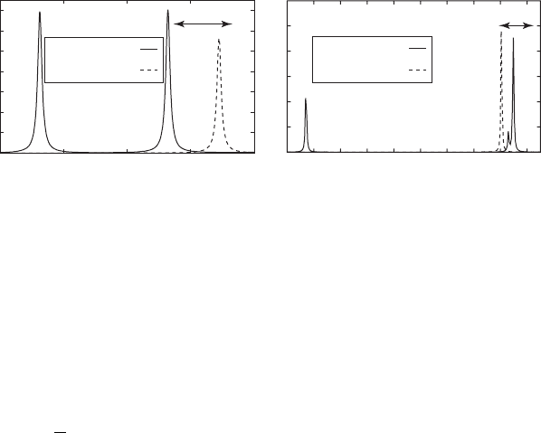
Figure 23.5 shows the optical response for a GaAs-based [23] (left panel) and GaN-based [24]
(right panel) two-QD structure. Spectra are calculated by exact diagonalization of the corre-
sponding many-body Hamiltonian [23] . The fi gure compares the calculated excitonic (solid line)
and biexcitonic (dashed line) spectra. Peak “ a ” corresponds to the creation of an exciton in the
fi rst dot, peak “ b ” to the creation of an exciton in the neighbouring dot – and corresponding exci-
ton–biexciton transitions are also seen (in the calculations of these exciton–biexciton lines, the
fi rst exciton is always created in QD
a
). As expected, the ground-state biexcitonic transition is blue
shifted for GaAs and red shifted for the GaN-based structure. Owing to the strong built-in electric
fi eld, the difference in energy between the two lowest excitonic transitions is one order of magni-
tude larger in GaN-based structures than in the GaAs ones.
exc. abs. sp.
biexc. abs. sp.
Δε
Δε
Ener
g
y (meV) Ener
g
y (meV)
ab
Absorption (a. u.)
ba
ab ab
GaN/AlN
GaAs/AlAs
1680 1685 1690 3180 3200 3220 3240 326016751670
exc. abs. sp.
biexc. abs. sp.
Figure 23.5 Excitonic (solid line) and biexcitonic (dashed line) absorption spectra for a GaAs-based (left panel)
and GaN-based (right panel) two QD structure [28] . An in-plane fi eld E 75 kV/cm has been applied to the GaAs-
based structure.
We now describe how to perform a quantum gate in this system. Let us consider an encod-
ing in which
|0 〉
l
, corresponds to the absence of ground-state exciton in QD
l
and
|1〉
l
to the pres-
ence of ground-state exciton in QD
l
. The whole computational space is now spanned by the basis
||nn
ll
〉⊗〉
, with n
l
0, 1. By introducing the operator
ˆ
n
lll
||11〉〈
, the effective Hamiltonian
of the system can be written as:
Hn nn
ll
l
ll
l
l
u
εε
ˆˆˆ
∑∑
′′
′
1
2
Δ
(23.5)
where ε
l
is the energy of the ground-state exciton in QD
l
and Δ ε
ll
is the biexcitonic shift between
excitons in QD
l
;
and QD
l
. Equation 23.5 was fi rst proposed in [29] and has the same structure
of the effective Hamiltonian used in NMR-based quantum computation. According to this
Hamiltonian, a conditional two-qubit operation, the CNOT gate, can be achieved by a laser
π -pulse exploiting the energy renormalization of the ground state excitonic transition due to the
biexcitonic shift. The corresponding conditional dynamics is schematically shown in Fig. 23.6 ,
for the case of two QDs with an exciton already present in QD
a
. In general a π -rotation of the tar-
get qubit
n
b
is achieved by a laser π -pulse centred at the energy ε
b
Δ ε
ab
if and only if the state of
the control qubit is
l
a
. Since Δ ε
ab
3 meV, this CNOT gate can be performed on sub-picosecond
timescales. In order to see how this gate can create entanglement, consider the factorizable state
CH023-I046325.indd 694CH023-I046325.indd 694 6/27/2008 6:36:30 PM6/27/2008 6:36:30 PM
Optically Driven Schemes for Quantum Computation Based on Self-assembled Quantum Dots 695
(| ) |αβ010〉|〉⊗〉
aab
. If the CNOT is performed on it, we obtain
αβ|| |00 11〉⊗ 〉 |〉⊗ 〉
ab ab
,
which is maximally entangled [23] .
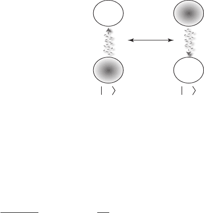
23.3.2.2 Foerster coupling
The Foerster interaction (which is also known as resonant energy transfer or dynamic dipole–
dipole coupling) was fi rst investigated in the context of sensitized luminescence of solids [30, 31] ,
but since then has been studied in many contexts including photosynthesis in biological systems
[32] and, of course, quantum information processing [33, 34] .
The process of resonant energy transfer of excitons is depicted schematically in Fig. 23.7 . The
easiest way to think of the process is as follows. Initially, an exciton is located on one of two adja-
cent quantum dots. It then recombines, emitting a photon, but this photon is quickly reabsorbed
by the second dot, and an exciton forms there. In fact, the photon is only ever a virtual particle,
so is not “ actually ” emitted. It can equivalently by thought of as an interaction between the tran-
sition dipoles of the two excitons and is thus sometimes called a dynamic dipole–dipole coupling.
In order to calculate the size of the coupling, an envelope function approximation is used to
describe the electron and hole wavefunctions:
ψφ
ppp
U() () ()rrr
(23.6)
ε
b
Δε
ab
h
a
e
a
e
a
h
b
h
a
e
b
QD
b
QD
b
QD
a
QD
b
QD
a
2.5 nm
x, yx, y
E
QD
a
2.7 nm
2.5 nm
zz
QD
b
2.5 nm
E
QD
a
2.7 nm
2.5 nm
ε
b
e
a
e
a
h
a
h
a
z
2.5 nm
E
2.7 nm
z
2.5 nm
x, yx, y
E
2.7 nm
2.5 nm2.5 nm
Figure 23.6 Conditional dynamics of excitons for the case in which a ground state exciton is present in QD
a
. We
consider a suitable GaN-based structure. Due to the biexcitonic shift Δ ε
ab
between QD
a
and QD
b
, a ground state
exciton is excited in QD
b
if and only if the laser π -pulse is resonant with the renormalized transition energy
ε
b
Δ ε
ab
of QD
b
.
CH023-I046325.indd 695CH023-I046325.indd 695 6/27/2008 6:36:31 PM6/27/2008 6:36:31 PM
696 Handbook of Self Assembled Semiconductor Nanostructures for Novel Devices in Photonics and Electronics
where φ
p
( r ) is an envelope function describing the changing wavefunction amplitude of confi ned
states for particle type p over the dot region, and U
p
( r ) is the Bloch function which has the perio-
dicity of the atomic lattice. The matrix element describing the coupling is given by [33] :
V
e
R
OO
R
F
r
2
0
3
2
2
2
4
3
πee
III a a
||〈〉 〈〉
⎛
⎝
⎜
⎜
⎜
⎞
⎠
⎟
⎟
⎟
⎟
rrR()
(23.7)
where the term r
a
represents the atomic position operator expectation value:
〈〉
∫
rrrrr
a
UUd
eh
cell
() ()
(23.8)
which is the same for both dots and
Od
space
ie
i
h
i
φφ
∫
() ()rrr
(23.9)
is the overlap of electron and hole envelope functions on the appropriate dot i. Varying the choice
of quantum dot size and materials can signifi cantly affect the size of the overlap integral, allow-
ing the grower to tailor the size of this interaction. The distance between dots R also plays an
important part in determining the magnitude of the interaction, which varies as 1 /R
3
. A typical
spacing is around 5 nm [35] , and for other typical parameters, V
F
is of order 1 meV. This energy
sets a timescale for the transfer of an exciton on resonance of around 1 ps.
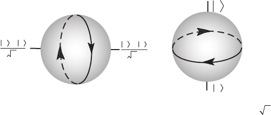
In order to understand how we can use Foerster transfer to perform an entangling gate, let us
consider the Hamiltonian for an exciton on either the right dot (state
|0 1〉
) or the left dot (state
|10〉
), coupled by the Foerster matrix element V
F
:
Hε ε |||||10 10 01 01 01 10〉〈 〉〈 〉〈|( ) ( ..)δ VHc
F
(23.10)
where e is the exciton energy for the left dot, and δ is the difference between the exciton creation
energies of the dots. δ 0 represents the resonant condition, and in this case the eigenstates of
the system are
21001
12
/
(| | )〉〉
. On the other hand, if δ V
F
, the eigenstates are
|0 1〉
and
|10〉
.
These two situations can again be pictured in the Bloch sphere representation, and this is shown
in Fig. 23.8 .
If we could move between these two different regimes, a procedure for creating an entangled
state would be as follows:
● Cool the double dot to its ground state (
|0 0 〉
).
● In the δ V
F
regime, apply a π pulse to the left dot, and so create the
|10〉
state.
● M o v e non-adiabatically to the δ 0 regime, and allow the system to evolve naturally. This
natural evolution is precession around the axis connecting the eigenstates (which now lie
in the equator of the Bloch sphere); the state is rotated towards the equator.
01 10
V
F
Figure 23.7 Drawing depicting Foerster coupling between two quantum dots. Excitons are shown in grey. If the
dots are resonant, an exciton on one dot will recombine, emitting a virtual photon that creates an exciton on the
second dot.
CH023-I046325.indd 696CH023-I046325.indd 696 6/27/2008 6:36:31 PM6/27/2008 6:36:31 PM
Optically Driven Schemes for Quantum Computation Based on Self-assembled Quantum Dots 697
● Move back to the δ V
F
regime once the state of the system is in the equatorial plane of
the Bloch sphere. This state is maximally entangled and remains so.
Further, in a completely analogous way, a general entangling gate can be performed.
However, we must be able to move between the two regimes to do this. One possible method
could be to apply an electric fi eld to both dots, which as we have seen shifts the hole in one direc-
tion and the electron in the other. This reduces the overlap integral between them, and therefore
the Foerster coupling. However, this can only be done slowly in practise, and the degree of modu-
lation is typically only a few per cent (see [34] ). It is more practical to tune the energies of the
excitons to vary δ – and thus change the effectiveness of the Foerster coupling. This can be done
using the AC Stark effect [36] when a detuned laser is applied to the excitonic transition, which
rather than altering the state of the system changes its energy. The exciton creation energy is
Stark shifted by an amount:
Δ
Ω
e
2
4ν
(23.11)
where Ω is the exciton–laser coupling and ν is the laser detuning. Each of the two dots have non-
identical Ω and ν and so shift by different amounts, even when illuminated by the same laser.
By applying fast laser pulses it is possible to tune two dots in and out of resonance on the sub-
picosecond timescale.
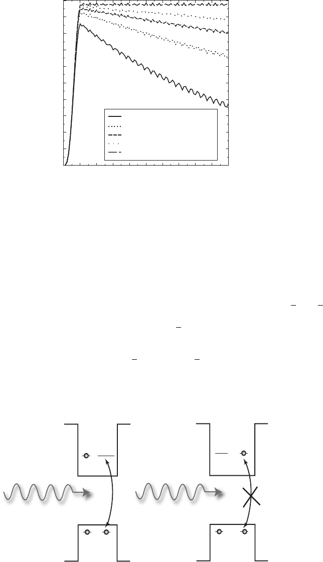
Figure 23.9 shows a simulation of quantum dynamics during a gate. We have plotted the
“ entanglement of formation ” as a function of time; this takes a value of unity for a maximally
entangled state, and zero for a completely unentangled one.
2
The plot shows that a maximally
entangled state can indeed be created using the recipe outlined above.
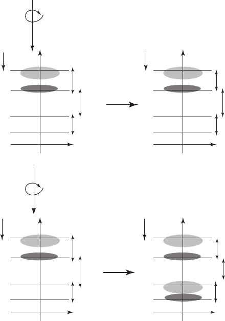
23.4 Spin representation
We now turn to self-assembled quantum dots in which an extra electron has been added through
either doping or the application of an external potential. Again, we look at the two requirements
for quantum computing: arbitrary single-qubit manipulation and an entangling two-qubit gate.
23.4.1 Single-qubit gates
The simplest method for performing arbitrary manipulation of a single electron spin proceeds
along similar lines to the manipulation of a single-exciton discussed in section 23.3.1. Typically,
the spin would be placed in a magnetic fi eld in order to induce a Zeeman splitting of the magnetic
sublevels. This splitting is typically on the micro-electron-volt level, and so the radiation needed
to resonantly excite the spin is a few GHz. The coupling is also much weaker than before, since it
proceeds via the magnetic (and not the electric) transition dipole. This means that the gates take
10
01
01
10
2
01
10
2
δ
V
F
V
F
δ
Figure 23.8 Bloch sphere picture of the |10, |01 subspace in different parameter regimes. By moving between
one regime and the other quickly, an entangling gate is effected. See text for details.
CH023-I046325.indd 697CH023-I046325.indd 697 6/27/2008 6:36:32 PM6/27/2008 6:36:32 PM
698 Handbook of Self Assembled Semiconductor Nanostructures for Novel Devices in Photonics and Electronics
much longer to perform than the optical gates discussed earlier. However, it turns out that it is
possible instead to use optical radiation to rotate a spin, and as we shall now show, this can be
much quicker than using microwaves.
In order to understand how this works, we must fi rst introduce the concept of Pauli blocking.
We show the basic principles of operation in Fig. 23.10 . The qubit has a spin of either
1
2
or
1
2
,
and we label these as qubit state
1
and
0
, respectively. The valence states are full, with the
highest lying electrons (lowest lying holes) having spin
3
2
. If a laser is applied with σ
polar-
ization, tuned to the transition energy between lowest hole and lowest electron, it can only be
absorbed if the QD system changes its angular momentum by 1. The only possible way this can
happen is if an electron is promoted from the
3
2
state to the
1
2
state. Owing to the Pauli exclu-
sion principle, such a transition is not possible if the system exists in qubit state
|0 〉
. On the other
hand,
|1〉
will happily couple to a three-particle entity called a trion (two electrons plus one hole).
|3/2> |3/2>
|1/2>
|1/2>
|1/2>
|1/2>
|3/2> |3/2>
1
σ
σ
0
Figure 23.10 Schematic diagram showing the Pauli-blocking effect. The left-hand drawing shows the excess
electron in the spin-up state (qubit |1), the right shows the electron spin down (qubit |0 ). Under illumination with
σ
light, a trion state ( |X) couples to |1, but not |0 .
0 5 10 15 20
No decay
25 30 35 40 45 50
t/ps
0.0
0.1
0.2
0.3
0.4
0.5
0.6
0.7
0.8
0.9
1.0
Entanglement of formation
t
1
331 ps, t
2
100 ps
t
1
1.65 ns, t
2
500 ps
t
1
3.3 ns, t
2
1 ns
t
1
826 ps, t
2
250 ps
Figure 23.9 Entanglement of formation as a function of time for a Foerster coupled double dot system under the
action of a laser [50] . The laser is pulsed on for 5 ns, and the AC Stark effect causes the dots to come on to resonance,
thus effecting an entangling operation. The entanglement is degraded when exciton decay is simulated, the decay being
characterized by time τ
i
for dot i . More details of the simulation are given in [50] .
CH023-I046325.indd 698CH023-I046325.indd 698 6/27/2008 6:36:32 PM6/27/2008 6:36:32 PM