Henini M. Handbook of Self Assembled Semiconductor Nanostructures for Novel devices in Photonics and Electronics
Подождите немного. Документ загружается.

Quantum Dot Infrared Photodetectors by Metal-Organic Chemical Vapour Deposition 639
of our QDIP were 1.0 1 0
10
cmHz
1/2
/W at a bias of 0.4 V at T 77 K and 1.0 1 0
9
c m H z
1/2
/
W at a bias of 0.3 V at T 1 0 0 K .
21.4.1.6 Quantum effi ciency
The internal quantum effi ciency of our QDIP was extracted using Eq. 21.15 in section 21.2 and
was found to be less than 0.1%.
21.4.2 InAs/AlInAs/InP QDIP
As shown above, the dark current of our InAs/InGaAs/InP QDIP is still very high. A high band
gap material such as AlInAs can act as a current blocking layer (CBL) and reduce the dark cur-
rent and improve the performance in the In(Ga)As/GaAs QDIP system. In this section, a device
structure with AlInAs CBL is used to reduce the dark current [21] .
3 2 1
0123
1E7
1E8
1E9
1E10
Peak detectivities at 77 K and 100 K
77 K
100 K
Detectivity (cmHz
1/2
/W)
Bias (V)
Figure 21.18 Specifi c detectivity vs bias for the ten stack InAs/GaInAs/InP QDIP at 77 K and 100 K.
3 2 10123
1E-13
1E-12
1E-11
1E-10
Noise currents at 77 K and 100 K
77 K
100 K
Noise current (A/Hz
1/2
)
Bias (V)
Figure 21.17 Noise current measured as a function of bias for the ten stack InAs/GaInAs/InP QDIP at 77 K and
100 K.
CH021-I046325.indd 639CH021-I046325.indd 639 6/27/2008 5:48:11 PM6/27/2008 5:48:11 PM
640 Handbook of Self Assembled Semiconductor Nanostructures for Novel Devices in Photonics and Electronics
First, a 0.5 μ m undoped InP buffer was grown at 590°C followed by a 0.5 μ m bottom InP con-
tact layer doped with dilute SiH
4
to n 1 10
18
cm
3
. Next, the active region was grown at
500°C. The active region consisted of 10 periods of the following structure: 400 Å InP barrier,
10 Å GaAs, InAs QDs, and 30 Å Al
0.48
In
0.52
As CBL. For InAs QDs, the nominal growth rate was
0.42 ML/s and the growth time was 12 seconds. After the QD layer was deposited, 60 seconds
of ripening time was given with dilute AsH
3
fl owing. The InAs QDs were doped with dilute SiH
4
(200 ppm) with a fl ow rate of 35 sccm. Finally, a 0.2 μ m n -type InP ( n 1 1 0
18
c m
3
) top con-
tact layer was grown at 590°C.
21.4.2.1 Dark current
The dark current ( I
d
) of a QDIP mesa was measured as a function of bias ( V
b
) at different tem-
peratures, as shown in Fig. 21.19 . Also shown is the 300 K background photocurrent with
a 45 ° fi eld of view (FOV). The background-limited performance (BLIP) was obtained at 100 K
for the 1 . 9 V V
b
3.7 V range. A very low dark current was observed for this QDIP due to
the Al
0.48
In
0.52
As CBL. At T 77 K, a dark current below the pA range was observed between
0.8 V and 1.8 V. An asymmetric I–V relationship was also observed in this QDIP, especially at
lower temperatures. The asymmetry of the dark current for our QDIP can be attributed to sev-
eral factors. First, it could be due to the asymmetry of the device structure as every GaAs/InAs/
AlInAs/InP period of the active region is asymmetric. Second, the InAs QD has a lens shape
which is not symmetric in the growth direction. Third, dopant diffusion into the quantum dot
layer during the material growth might create a small built-in electric fi eld. A complete under-
standing of the dark current characteristics of our QDIP needs further theoretical and experi-
mental investigation.
8 6 4 202468
10
1
10
2
10
3
10
4
10
5
10
6
10
7
10
8
10
9
10
10
10
11
10
12
10
13
10
14
10
15
10
0
300 K BG
Dark current (A)
Bias (V)
From bottom to top
273 K
250 K
220 K
190 K
160 K
140 K
110 K
100 K
77 K
Figure 21.19 Dark current measured as a function of bias for InAs/GaAs/AlInAs/InP QDIP at different tempera-
tures. Also shown is the 300 K background photocurrent with a 150 ° fi eld of view (dashed line).
21.4.2.2 Spectral response
The spectral response of the QDIP was tested on an FTIR spectrometer. Photoresponse peaked at
6.4 μ m with a cut-off at 6.6 μ m (see Fig. 21.20 ). The spectral width ( Δ λ / λ
peak
) was 12%, which
indicated bound-to-bound intersubband absorption. The shape, peak and cut-off of this QDIP
showed negligible change with varying temperature (from T 7 7 K t o T 160 K) and bias (from
V
b
1 V t o V
b
3 V).
CH021-I046325.indd 640CH021-I046325.indd 640 6/27/2008 5:48:12 PM6/27/2008 5:48:12 PM
Quantum Dot Infrared Photodetectors by Metal-Organic Chemical Vapour Deposition 641
21.4.2.3 Responsivity
Peak responsivity ( R
p
) at both 77 K and 100 K are shown in Fig. 21.21 . An asymmetry was also
observed for the peak responsivity, both at 77 K and 100 K. The asymmetry of the responsivity is
caused by the asymmetry of the potential in the QD itself. At T 77 K and bias of 5 V, a peak
responsivity of 1.0 A/W was observed for our QDIP.
510152025
0.0
0.5
1.0
Photoresponse (a.u.)
Wavelength (μm)
T 77 K
Bias 1.0 V
λ
peak
6.408 μm
λ
cut-off
6.637 μm
Figure 21.20 The relative spectral response measured at bias of 1 V and temperature of 77 K.
8 6 4 20246
10
3
10
2
10
1
10
0
10
1
10
2
10
3
100 K
77 K
Responsivity (mA/W)
Bias (V)
Figure 21.21 Peak responsivity as a function of bias for the QDIP at 77 K and 100 K.
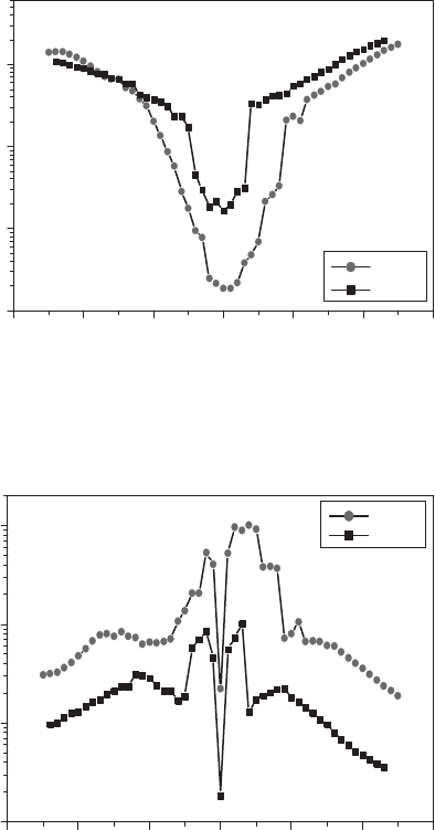
21.4.2.4 Noise current
As shown in Fig. 21.22 , very low noise was observed and was almost constant for biases
1 . 0 V V
b
2.5 V at 77 K and 0.8 V V
b
2.3 V at 100 K. Beyond these ranges, the noise
was dominated by generation–recombination noise of the dark current. Based on the measured
noise current and dark current ( i
d
), we extracted the gain g of the device using i
n
2
4 egI
d
for unit
bandwidth. The gain of the device depends strongly on the bias and increases from 5 to 5000
when the bias changes from 1.2 V to 3.5 V. The high value of the gain in a given voltage
range is a unique feature of this QDIP technology. The gain in our QDIP devices is much higher
than the gain measured in typical quantum well infrared detectors.
CH021-I046325.indd 641CH021-I046325.indd 641 6/27/2008 5:48:13 PM6/27/2008 5:48:13 PM
642 Handbook of Self Assembled Semiconductor Nanostructures for Novel Devices in Photonics and Electronics
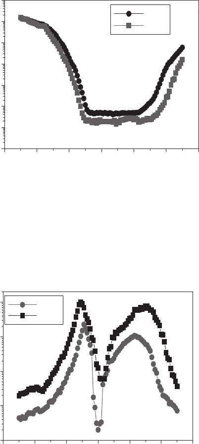
21.4.2.5 Detectivity
The detectivities of our QDIP as a function of bias at both T 77 K and T 100 K are shown in
Fig. 21.23 . The highest detectivities of our QDIP were 1.0 1 0
10
c m H z
1/2
/W at a bias of 1 . 1 V
and 2.3 1 0
9
cmHz
1/2
/W at a bias of 0.9 V for T 77 K and T 100 K, respectively.
10
8
10
9
10
10
10
11
10
12
10
13
10
14
10
15
6 4 20246
100 K
77 K
Noise (A/Hz
1/2
)
Bias (V)
Figure 21.22 Noise current as a function of bias at 77 K and 100 K.
100 K
77 K
6 4
2
0246
Detectivity (cmHz
1/2
/W)
Bias (V)
10
10
10
9
10
8
10
7
10
6
Figure 21.23 Peak detectivity as a function of bias at 77 K and 100 K.
21.4.2.6 Quantum effi ciency
The internal quantum effi ciency ( η ) of our QDIP was calculated and was found to be less than
0.1%. The very low quantum effi ciency so far is due to the (i) low oscillator strength for s -polarized
light, (ii) less-than-unity fi ll factor of the quantum dot layer and (iii) a thin active region of ten
layers of QDs. A low oscillator strength must be expected for s -polarized light in a fl at (50 nm by
5 nm) lens-like QD at this wavelength. The quantum effi ciency can be improved by increasing dot
density, optimizing the dot shape, size and uniformity [22] .
CH021-I046325.indd 642CH021-I046325.indd 642 6/27/2008 5:48:14 PM6/27/2008 5:48:14 PM
Quantum Dot Infrared Photodetectors by Metal-Organic Chemical Vapour Deposition 643
21.4.3 MWIR InP-based QDIP
Our world fi rst InP-based InAs QDIPs with high detectivity have a peak detection wavelength of
6.4 μ m. The wavelength 6.4 μ m is outside the MWIR(3 ~ 5 μ m) or LWIR (8 ~ 12) μ m window
where there is low absorption in the atmosphere. As has been shown in the previous section, the
size and shape of the quantum dot can be changed by varying the growth conditions. In this sec-
tion, the peak detection wavelength of QDIP is tailored by dot engineering in order to achieve an
MWIR QDIP.
21.4.3.1 Optimization of the single-layer QD growth
In order to have QDs that will detect shorter wavelength in the MWIR range, the QD growth
conditions were thoroughly optimized again as in section 21.3, but specifi cally for the goal to be
smaller size, high density, and high uniformity QDs. Growth parameters including growth tem-
perature, growth rate, V/III ratio and ripening time have been optimized.
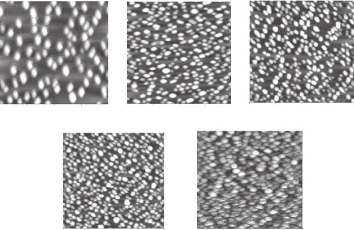
First, growth temperature was studied again but in a broader range between 440
o
C and 520
o
C
with an interval of 20
o
C. The AFMs of a single-layer QD grown at these temperatures are com-
pared in Fig. 21.24 . It is clearly seen that the dot size decreases and the dot density increases with
the decrease of the growth temperature. The growth temperature of 440
o
C was chosen.
Next, the growth rate of the QD was studied. The growth rate was varied by varying the
fl ow rate of the group III precursor, in this case TMIn. Three fl ow rates were used: 50, 100 and
150 sccm. The corresponding growth time was adjusted to make the total amount of material
deposited (the product of the TMIn fl ow rate and growth time) the same. The rest of the growth
conditions were identical. The dot density was checked with AFM and Fig. 21.25 shows the dot
density as a function of the fl ow rate of TMIn. It is shown that higher growth rate gives higher
dot density. Although 150 sccm gives a slightly higher dot density, PL shows that 100 sccm has
better quality. Thus 100 sccm was used for optimization after.
0 0.25 0.50
0.75
1.00
520°C
0 0.25 0.50 0.75 1.00
m m
460°C
1.00
0.75
0.50
0.25
0
440°C
0 0.25 0.50 0.75 1.00
1.00
0.75
0.50
0.25
0
500°C
0.250 0.50 0.75 1.00
480°C
0 0.25 0.50
0.75
1.00
Figure 21.24 AFM images of single-layer InAs QDs grown at different temperatures.
CH021-I046325.indd 643CH021-I046325.indd 643 6/27/2008 5:48:16 PM6/27/2008 5:48:16 PM
644 Handbook of Self Assembled Semiconductor Nanostructures for Novel Devices in Photonics and Electronics
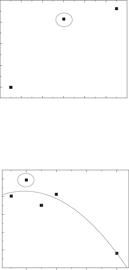
The V/III ratio was optimized by varying the fl ow rate of the group V precursor: 5% dilute
arsine. The fl ow rates of 25, 50, 75, 100 and 200 sccm were used. The fl ow rate of TMIn was
100 sccm. Dilute arsine gives the highest dot density of 50 sccm as shown in Fig. 21.26 and was
chosen for the growth after.
300
40 60 80 100 120 140 160
350
400
450
500
Dot density (m
2
)
Flow rate of TMIn (sccm)
Figure 21.25 Dot density as a function of the trimethylindium fl ow rate.
300
350
400
450
250
100 15050 200
500
Dot density (m
2
)
Flow rate of dilute arsine (sccm)
Figure 21.26 Dot density as a function of V/III ratio.
Next, the ripening time is optimized. The ripening time is the time that needs to elapse after
the dot material was deposited and before it is covered by the next layer. Usually it is used to allow
the dot to form, or to “ ripen ” . Ripening times of 60, 30, 10 and 0 s were used to study its effect
on the dot formation. For this optimization, the method used so far, of single-layer uncapped QDs
scanned by AFM, is no longer a good characterization technique because during the cooling down
after growth, the QDs on the surface may still change when it is hot. Instead, a cap layer after QD
growth (as in the device growth) was to be grown after ripening, then the samples were studied
with photoluminescence (PL).
CH021-I046325.indd 644CH021-I046325.indd 644 6/27/2008 5:48:20 PM6/27/2008 5:48:20 PM
Quantum Dot Infrared Photodetectors by Metal-Organic Chemical Vapour Deposition 645
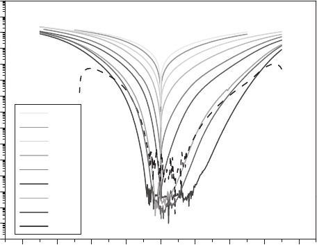
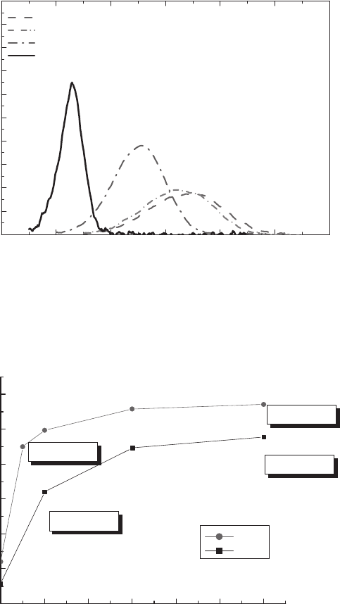
Figure 21.27 shows the room temperature PL of QDs grown at 440
o
C with different ripen-
ing times. Several trends can be seen here with the decrease of the ripening time from 60 s to
0 s. First, there is clearly a blue shift, which indicates smaller dot size. Second, the full width half
maximum (FWHM) decreases, indicating better uniformity. Finally, the intensity is higher which
indicates higher dot density and quality. The same study was also done for the QDs grown at a
higher temperature of 500
o
C and similar trends were observed but with a shift of the PL peak
toward a longer wavelength ( Fig. 21.28 ). This is clearly the result of the larger dot size at higher
growth temperature, as shown by Fig. 21.24 .
0.00
1000 1200
1400
1600
1800 2000 2200
0.02
0.04
0.06
0.08
0.10
0.12
0.14
0.16
0.18
0.20
1995: 60 s λ 1678 nm FWHM 143 meV A 11.71658 H 0.03474
1999: 30 s λ 1646 nm FWHM 134 meV A 11.81476 H 0.03816
2000: 10 s λ 1520 nm FWHM 120 meV A 18.11168 H 0.07617
2001: 0 s λ 1258 nm FWHM 72 meV A 13.71036 H 0.13004
RT PL of InAs QD grown @ 440C
Intensity (a.u.)
Wavelength (nm)
Figure 21.27 Room temperature PL of four InAs QD samples (#1995, 1999, 2000 and 2001) grown at 440
o
C
with ripening times of 60, 30, 10 and 0 s, respectively. Note the change of the wavelength λ , FWHM, integrated
intensity A (for area) and peak intensity H (for height) with the decrease in the ripening time.
PL peak wavelength from single QD layer
1200
20 30 40 50 60010
1300
1400
1500
1600
1700
1800
5.0 m QDIP
6.0 m QDIP
4.2 m QDIP
6.4 m QDIP
1771
1758
1697
1650
1320
1678
1646
1520
1258
PL peak wavelength (nm)
Ripening time (s)
500°C
440°C
Figure 21.28 PL peak wavelength as a function of the ripening time for QDs grown at 440
o
C and 500
o
C.
CH021-I046325.indd 645CH021-I046325.indd 645 6/27/2008 5:48:21 PM6/27/2008 5:48:21 PM
646 Handbook of Self Assembled Semiconductor Nanostructures for Novel Devices in Photonics and Electronics
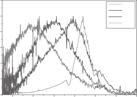
As can be seen in Fig. 21.28 , with the combination of the growth temperature and ripen-
ing time, the PL peak wavelength can be tuned in a wide range. However, detection in QDIPs is
caused by the intersubband transition rather than the interband transition in PL. Thus it is nec-
essary to check the tunability of dot detection wavelength with FTIR. Figure 21.29 shows that
peak detection wavelengths from 4 μ m to 6.4 μ m have been obtained by changing the growth
temperature and ripening time. At 500°C, the minimum wavelength that can be reached is
around 6 μ m with even 0 s ripening time. At 440°C, the 4 μ m and 5 μ m were obtained with 10
and 60 s ripening times.
0.2
0.4
0.6
0.8
1.0
0.0
1.2
4
5
6
78
3
9
4 m
5 m
5.9 m
6.4 m
1959
1625
2022
2009
Photoresponse (a.u.)
Wavelength (m)
Figure 21.29 Photocurrent spectra of QDIPs with different detection wavelengths.
21.4.3.2 Optimization of the multi-stack QD growth
As shown above, in order to have an MWIR QDIP, at least the QD and the adjacent layer have to
be grown at 440°C. One concern is that if the InP barrier is grown at such a low temperature
(note the optimum growth temperature for InP in this work is around 590°C, as shown in the
previous section) the barrier quality would be poor. This will have two consequences: fi rst, the
surface after the barrier growth will be rough (as proven by the AFM image of the surface of a
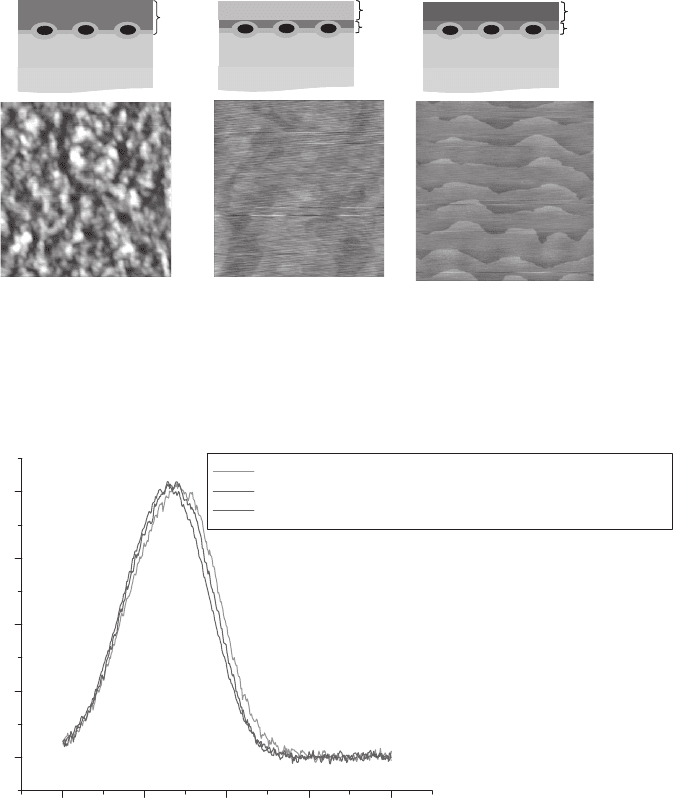
40 nm InP barrier grown at the 440°C on the left in Fig. 21.30 ). As a result, the next QD layers
will be grown on a much different surface compared with the fi rst QD layer. This will cause the
non-uniformity of QDs at different layers and the degradation of quality with the increase of the
QD layers. Second, the barrier grown at low temperature may have poor electronic and optical
quality. Hall measurements of the InP grown at 500°C and 440°C have shown orders of magni-
tude in higher background concentration compared with that grown at 590°C. This may lead to
high dark current. In order to solve this problem, a two-temperature barrier growth technique
is used. As shown in Fig. 21.30 , after the QD growth, a thin InP layer with a thickness of 10 nm
is grown at the same temperature as the QD and then the temperature is ramped up and the rest
of the barrier is grown at a higher temperature, 500°C and 590°C, respectively. The AFM scans
show clearly that with this technique, the morphology improves: the roughness (RMS) of the
three samples is 9 Å, 3.9 Å and 1.24 Å, respectively. Atomic steps are seen for the 500°C barrier
(in the middle) and are very clear at 590°C (on the right). The surface for the InP barrier grown
with 590°C is almost the same as the InP before the fi rst QD layer, which indicates the reproduc-
ibility of QD at the next layer.
With this two-temperature technique, another concern arises: will the high temperature affect
the QD by annealing? In order to check this effect, PLs of the above three samples were measured
and the result is shown in Fig. 21.31 . The two-temperature growth causes an almost negligible
CH021-I046325.indd 646CH021-I046325.indd 646 6/27/2008 5:48:21 PM6/27/2008 5:48:21 PM
Quantum Dot Infrared Photodetectors by Metal-Organic Chemical Vapour Deposition 647
blue shift and almost the same FWHM, indicating there is almost no effect of the high tempera-
ture on the dot properties such as size, shape and composition.
21.4.3.3 Device results
With the QD growth conditions optimized, three devices with different QD growth conditions were
grown. An Emcore LP-MOCVD reactor was used to grow QDIP device structures. Trimethylindium
and triethylgallium were used as group III precursors while pure phosphine, pure arsine and
5% dilute arsine were used as group V precursors. The typical device structures are as follows.
First, a 0.5 μ m undoped InP buffer layer was grown at 590
o
C followed by a 0.5 μ m bottom InP
contact layer doped with dilute SiH
4
to n 1 1 0
18
c m
3
, then the active region which is
a ten-period quantum dot layer separated by InP barriers, and a 0.2 μ m top Ga
0.47
In
0.53
As
contact layer doped with dilute SiH
4
to n 5 1 0
17
c m
3
. The structure of device A is
0.00
1400 1600 1800 2000 2200
0.05
0.10
0.15
0.20
Intensity (a.u.)
Wavelen
g
th (nm)
1-temp (440C): λ 1678 nm FWHM 112 meV
2-temp (440C 500C): λ 1656 nm FWHM 108 meV
2-temp (440C 590C): λ 1656 nm FWHM 112 meV
Figure 21.31 Room temperature PL single-layer InAs QD covered with 40 nm InP barrier grown at different
conditions.
RMS 0.900 nm
No atomic steps
RMS 0.391 nm
Atomic steps but less
regular
RMS 0.124 nm
Clear atomic steps as
good as bulk InP
SI InP substrate
InP buffer
40 nm InP barrier
440°C
SI InP substrate
InP buffer
30 nm InP
500°C
440°C
590°C
SI InP substrate
InP buffer
30 nm InP
440°C
Figure 21.30 Comparison of AFM for the InP barrier after InAs QD. Left: 40 nm InP barrier grown at the same
temperature of 440°C as QDs. Middle : 10 nm InP grown at 440°C plus 30 nm InP grown at 500°C. Right: 1 0 n m
InP grown at 440°C plus 30 nm InP grown at 590°C.
CH021-I046325.indd 647CH021-I046325.indd 647 6/27/2008 5:48:22 PM6/27/2008 5:48:22 PM
648 Handbook of Self Assembled Semiconductor Nanostructures for Novel Devices in Photonics and Electronics
similar to that of the InAs/AlInAs/InP QDIP discussed above in section 21.4.2. Its active region
was grown at 500
o
C. The active regions of the other two devices (device B and device C) were
grown using the two-temperature technique. The InAs QDs of device B and C were grown at
440
o
C. The nominal growth rate was 0.84 ML/s and the growth time was 6 s. The InAs QDs of
device B were grown on InP barriers which were grown at 590
o
C. On the other hand, the QDs
of device C were grown on 3 nm Al
0.48
In
0.52
As/InP barriers which were grown at 590
o
C. Before
the deposition of InAs layers in device B and C, thin 1 nm GaAs layers were inserted on the InP
or Al
0.48
In
0.52
As in order to produce more uniform QDs as in device A [23] . The growth inter-
ruption time after the QD growth was 30 s under dilute AsH
3
fl owing. After the 30 s interruption,
the fi rst 10 nm InP capping barriers were grown at 440
o
C and the remaining 30 nm InP barri-
ers were grown at 590
o
C. The reason why we used two-temperature barrier growth is because
we were able to improve the InP barrier quality which in turn leads to a decrease in the dark
currents.
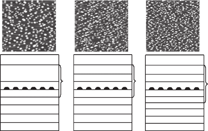
Device A
S.I. InP substrate
100Å InP
500°C 10Å GaAs
500°C InAs QDs
500°C 400Å InP
10
0.5 m InP buffer layer
0.2 m Ga
0.47
In
0.53
As
0.5 m n
InP
S.I. InP substrate
100Å InP
440°C 10Å GaAs
440°C InAs QDs
440°C 100Å InP
590°C 300Å InP
10
0.5 m InP buffer layer
0.2 m Ga
0.47
In
0.53
As
0.5 m n
InP
Device B
S.I. InP substrate
100Å InP
30Å AI
0.48
In
0.52
As
440°C 10Å GaAs
440°C InAs QDs
440°C 100Å InP
590°C 300Å InP
10
0.5 m InP buffer layer
0.2 m Ga
0.47
In
0.53
As
0.5 m n
InP
Device C
Figure 21.32 The 1 μ m 1 μ m AFM images of the single layer of uncapped InAs QDs corresponding to the struc-
tures of device A, B and C. In the AFM images, the data scale of the height is 10 nm.In the device structures, the shown
temperature is the growth tem1perature and if the temperature is not shown, the growth temperature is 590
o
C .
The schematic diagrams of device A, B, and C and 1 μ m 1 μ m AFM images of QDs correspond-
ing to each device are shown in Fig. 21.32 . The density of InAs QDs is around 3~5 1 0
10
c m
2
.
The InAs QDs of device A have a lens-like shape with a typical base diameter of 50 nm and a
height of 5 nm, and those of device B and C have a similar shape with a typical base diameter of
50 nm and a height of 4 nm which is smaller than the height of QDs of device A. The decrease of
the height is caused by the different growth temperature and growth rate of QDs.
To test the performance of the QDIPs, 400 μ m 400 μ m detector test mesas were fabricated as
before. The samples were then mounted to a copper heat-sink and attached to the cold fi nger of a
liquid nitrogen cryostat equipped with a temperature controller.
The spectral response of the QDIP was tested by FTIR. The source light was normally incident.
The bias is applied to the top contact and the bottom contact is always grounded. In Fig. 21.33 ,
CH021-I046325.indd 648CH021-I046325.indd 648 6/27/2008 5:48:23 PM6/27/2008 5:48:23 PM