Gupta D. (Ed.). Diffusion Processes in Advanced Technological Materials
Подождите немного. Документ загружается.

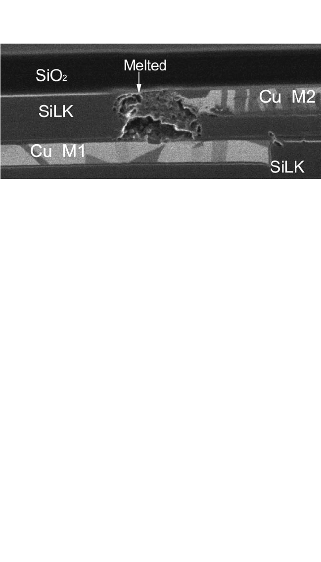
Figure 9.48 is a FIB image of the 0.21-mm-wide M2 line from the short-
lifetime group; it shows a void at V1M2 (open fail). The failure time of
64 hours at 298°C in the short-lifetime group is consistent with the time
to grow a 0.3-mm-long void at the cathode end of the 0.21-mm-wide line
with a blocking boundary as measured in CuSiO
2
structures. However, in
the case of the long-lifetime group, the voids were not observed at either
end of the 0.21-mm-wide M2 in most of the samples. No visible voids at
the V1 viaM1 interface are seen, as shown in Fig. 9.49(a), even though
the line was stressed for 585 hours. However, a void in the 3-mm-wide M1
short line is shown in Fig. 9.49(b). Voids in the 3-mm-wide M2 lines are
also often observed. For an electromigration drift velocity (Cu mass
migration rate) at 298°C of 0.006 mmh for the 0.21-mm-wide line, after
a lifetime of 600 hours, we would expect to see a 3.5-mm-void in the fine
M2 test line of Fig. 9.49(a) if the liner at the V1M1 interface were a
blocking boundary. In fact, no voids were observed near the M1V1
viaM2 interfaces in most of the tested samples. This result suggests that
the migration of Cu in the fine M2 line is replenished by the wide M1 line
through the V1 via. However, voids were found in the 3-mm-wide M1 and
M2, and some were observed at the end of the M1 section where there was
little or no electrical field, as shown in Fig. 9.49(b). Similar behavior has
been reported in AlSiO
2
[104, 117, 118]
and CuSiO
2
[40, 45]
During electromi-
gration, the Cu atoms will drift along the CuSiN
x
interface (the top Cu
surface), and the depletion of atoms is responsible for creating the voids.
Thus, voids would be expected to occur at the cathode ends of the fine M2
lines. However, a large portion of the tested samples showed no voids at
the fine M2V1 via interface in the long-lifetime group. The mass trans-
port of Cu toward the anode along the top M2 surface generates excess
472 DIFFUSION PROCESSES IN ADVANCED TECHNOLOGICAL MATERIALS
Figure 9.48 FIB image of a failed sample from the short-lifetime group, showing
an open failure at the M2/V1.
Chapter-09 11/29/04 6:51 PM Page 472
ELECTROMIGRATION IN CU THIN FILMS, HUETAL. 473
vacancies and tensile stress near the cathode. The vacancy concentration
and stress gradients generate a vacancy flux that moves to vacancy sinks
such as interfaces, grain boundaries, or the ends of the M1 and M2 lines
to form voids. Some vacancies pile up at the end of the M2 and some
migrate through to M1, resulting in short and long lifetimes, respectively.
This may be rationalized by the following discussion.
If the liners at the V1M1 interfaces were good blocking boundaries,
mass accumulation at the anode end of the M1 lines should occur. This
electromigration-induced mass accumulation would generate a stress gra-
dient in a line that can cancel out the electromigration driving force,
Z
*
erj Ω(∆sL
c
), where Ω, ∆s, and L
c
are the Cu atomic volume,
electromigration-induced stress, and critical length, respectively. No dam-
age should occur in a metal line length below L
c
. The estimated value of
L
c
is 20 mm for an unpassivated Cu line with j at 2.6 mAmm
2
(jL
c
of
530Acm).
[91]
However, the observation of voids in 12-mm-long M1 lines
with 2.6 mAmm
2
supports the notion that thin liners at M1V1 interfaces
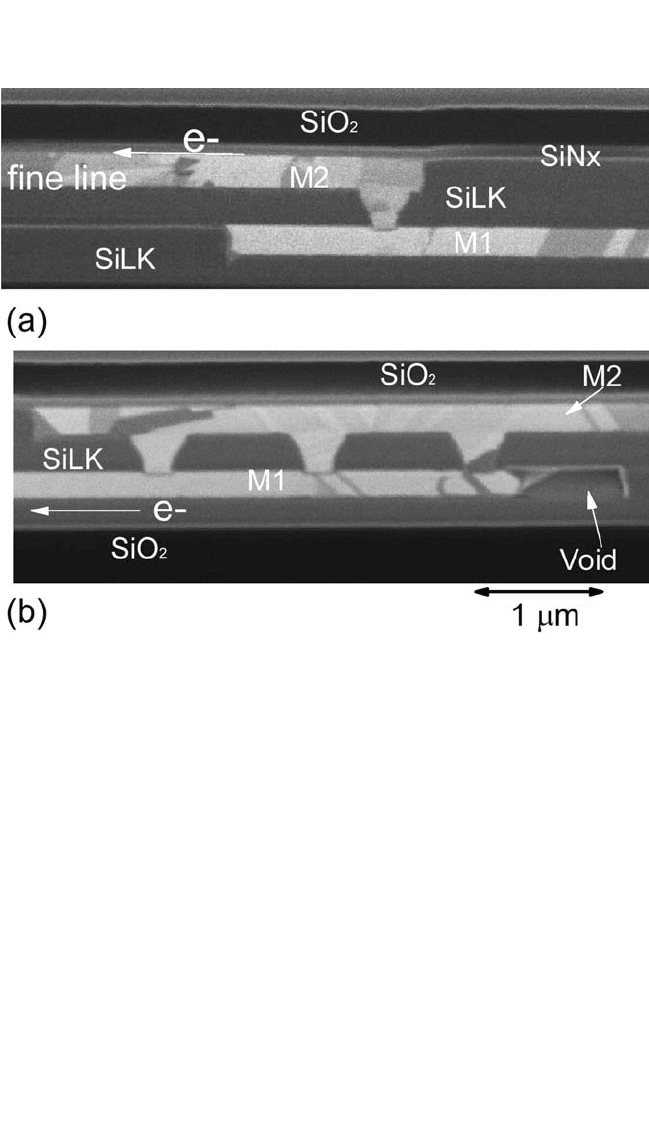
Figure 9.49 FIB images of a line tested at T = 298°C for 585 hours. (a) M1/V1/M2
fine test line interface; (b) wide M2 and M1 lines.
Chapter-09 11/29/04 6:51 PM Page 473

used in the present test structure cannot withstand the incoming Cu elec-
tromigration flux and Cu migration becomes continuous through M1 to
V1. Then the failure mechanisms in this structure are similar to that of
testing a fine test line connecting two large reservoirs at both ends of the
line; that is, continuous or partial flow will enable a very long lifetime.
However, with the anode end of the line connected to a blocking
boundary, such as a thicker liner or W via, high threshold values of jL
c
,
8000 Acm,
[77]
4000 Acm,
[123]
3000 Acm,
[124]
and 7000 Acm
[125]
for
lines with electron flow to a blocking boundary have been obtained.
Electromigration in two-level Cu dual-damascene lines in a low-
dielectric-constant material (SiLK dielectric) has been discussed. The fail-
ure distribution cannot be fitted to a single log-normal distribution. At
least two distinguishable lifetime groups were observed. The short-
lifetime group is consistent with the time required to grow a line void at
the end of the 0.21-mm-wide test line. The results are also in a good agree-
ment with the lifetimes obtained from the CuSiO
2
system. The samples
with lifetimes in the long-lifetime group suggest that the migration of Cu
in the M2 is replenished by Cu from the M1 through the V1M1 interface.
These observed results suggest that the fundamental CuSiLK dielectric
electromigration failure modes are similar to CuSiO
2
and that the
observed bimodal distribution is not the result of using a low-dielectric-
constant material. A thin liner at the Cu viaCu line interface that cannot
withstand the incoming Cu fluxes can also eliminate the short-length
effect in a Cu line.
9.13 Reduced Cu Interface Diffusion
As discussed in Secs. 9.10 through 9.12, the electromigration Cu life-
time is most dependent on atomic transport at the Cu/dielectric interface.
Some investigators have, however, reported that the Cu/liner interface is
the dominant fast path. There may be significant differences in the inte-
gration processes and materials, leading to differences in the interfaces.
However, in both cases, the fraction of total Cu atoms situated on inter-
faces increases as the dimension of the interconnection is scaled down.
Accordingly, the Cu electromigration lifetime and the allowed current
density specification in Cu conductors may be reduced in every new gen-
eration of interconnect. The ability to significantly extend Cu conductor
technology to smaller dimensions can be realized by altering or modify-
ing the Cu/dielectric interface to reduce the Cu transport properties; for
example, 50-nm-thick CoP
[126]
or 100 to 200-nm-thick CoWP
[127, 128]
selectively deposited electroless films can serve as diffusion barrier lay-
ers. Recently, improved electromigration Cu lifetime was reported from
474 DIFFUSION PROCESSES IN ADVANCED TECHNOLOGICAL MATERIALS
Chapter-09 11/29/04 6:51 PM Page 474
ELECTROMIGRATION IN CU THIN FILMS, HUETAL. 475
testing Cu lines with a thin (10 to 20 nm) surface layer of electroless
CoWP, CoSnP, or Pd.
[129]
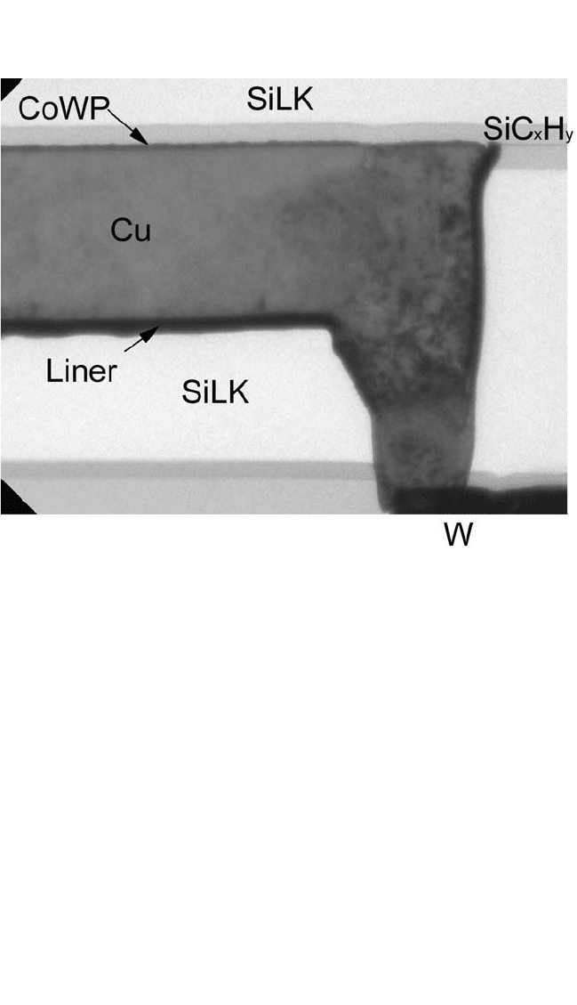
Figure 9.50 shows a TEM image of a 10-nm-
thick CoWP film on top of a Cu M1 line. The amorphous a-SiC
x
H
y
cap-
ping layer and a low-dielectric-constant (k 2.6) SiLK dielectric are
also shown. Asmooth, uniform layer of CoWP and large Cu grains were
observed. From this TEM sample, an x-ray energy dispersive spec-
troscopy (EDS) line scan was taken across the top Cu M1 surface.
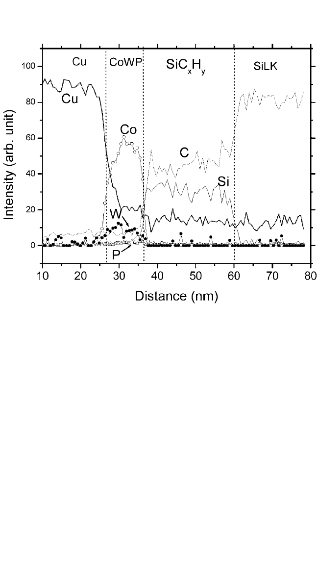
Figure 9.51 shows a plot of x-ray intensity as a function of element and
probe position for the line scan. The scan started in the Cu line near the
top surface, proceeded across the CoWP and amorphous SiC
x
H
y
layers,
and ended in the SiLK dielectric. In Fig. 9.51, the boundaries of these
layers are labeled. The EDS line scan shows that the Cu signal extends
somewhat into the CoWPlayer, suggesting that Cu is mixed into the cap.
The Cu signal remains above background noise counts even in the amor-
phous SiC
x
H
y
and SiLK dielectric layers because the samples were
mounted on a membrane on a Cu grid. Spurious X-rays hitting the Cu
grid provided a background Cu signal. The CoWPgrain size was measured
Figure 9.50 TEM cross-section image of a Cu interconnect coated with CoWP
using a Fig. 9.3(d) test structure.
Chapter-09 11/29/04 6:51 PM Page 475
to be 15 to 20 nm from a series of plan-view TEM images. The RBS
analyses determined the composition of the CoWP metal cap to be
Co(3% W, 6% P). Electromigration was performed on test structures of
either single-damascene Cu lines in SiO
2
on W or dual-damascene Cu
lines in SiLK on W. The metal linewidths ranged from 0.1 to 2 mm. The
current densities in the via bottom and line were 120 and 35 mA/mm
2
,
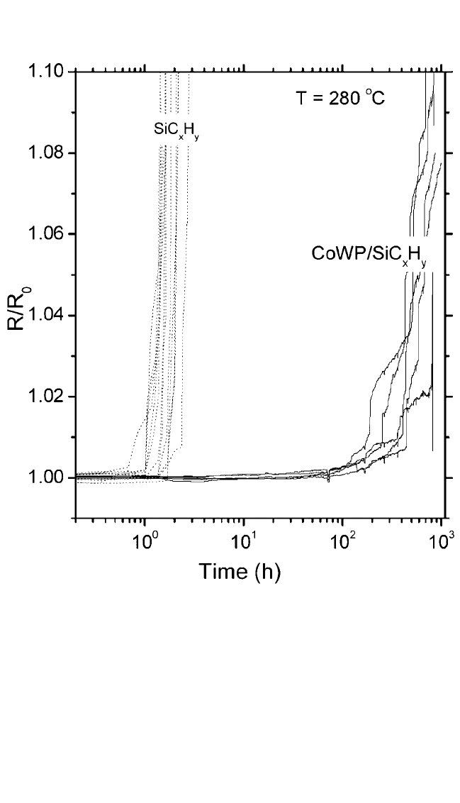
respectively. Figure 9.52 shows typical dual-damascene Cu test line
resistance as a function of time for 2-mm-wide polycrystalline lines
tested with CoWPa-SiC
x
H
y
and a-SiC
x
H
y
-only thin cap layers in SiLK
dielectric at a sample temperature of 350°C. The data clearly show a
remarkable improvement in lifetime for samples with CoWP coatings.
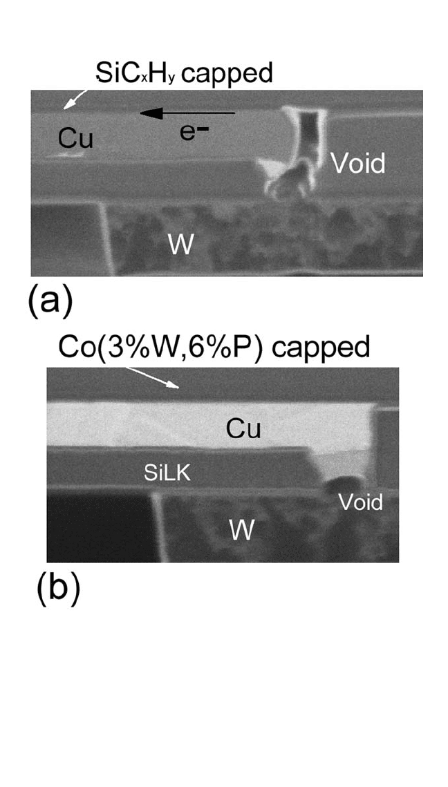
Voids were observed in the via bottom and/or the line in dual-damascene
Cu lines with an a-SiC
x
H
y
-only cap. However, only via bottom voids
were observed in the case of a CoWPcap. Figure 9.53(b) shows a via bot-
tom void for a Cu dual-damascene line with a CoWP cap.
476 DIFFUSION PROCESSES IN ADVANCED TECHNOLOGICAL MATERIALS
Figure 9.51 Intensities of elements from EDS measurements.The electron probe
moved from the top surface of a Cu damascene line, through the CoWP and amor-
phous SiC
x
H
y
coating layers, and ended in the SiLK dielectric.The vertical dotted
lines indicate the boundaries between the layers.
Chapter-09 11/29/04 6:51 PM Page 476
ELECTROMIGRATION IN CU THIN FILMS, HUETAL. 477
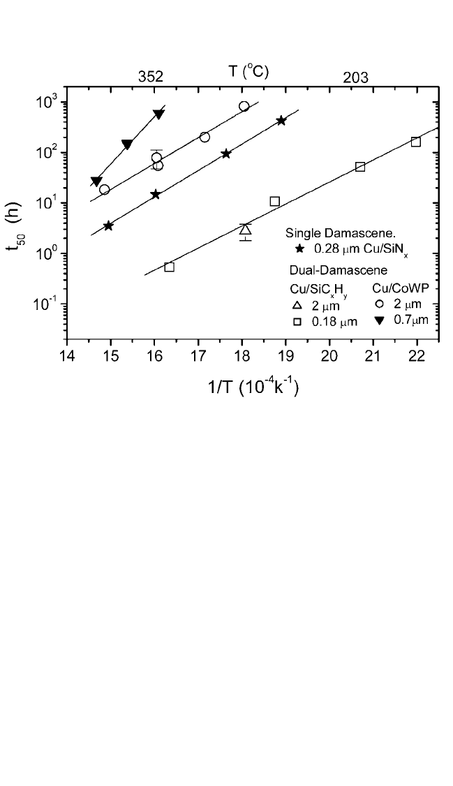
Figure 9.54 shows an Arrehenius plot of the median lifetimes of Cu
damascene lines with various capping layers. For comparison, the data
points from the samples of 0.27-mm-wide single-damascene lines capped
with SiN
x
are also included in Fig. 9.54. The solid lines are the least-
squares fits. The value of electromigration activation energy for 2-mm-
wide dual-damascene CoWPcapped polycrystalline lines was found to be
1.0 ± 0.1 eV. In the case of lines with bamboo-like grains, the activation
energies of 0.90 ± 0.05 eV, 1.0 ± 0.1 eV, and 1.9 ± 0.2 eV were obtained
Figure 9.52 The resistance of a damascene Cu conductor, with and without a thin
metal film on the top surface, versus time.
Chapter-09 11/29/04 6:51 PM Page 477
for a 0.18-mm-wide a-SiC
x
H
y
capped dual-damascene line, 0.27-mm-wide
SiN
x
capped single-damascene line, and a 0.7-mm-wide CoWP capped
dual-damascene line, respectively. Significant lifetime improvement for
the samples with CoWP capping compared to SiN
x
or a-SiC
x
H
y
capping
suggests that CoWP coating significantly reduces Cu diffusion along the
478 DIFFUSION PROCESSES IN ADVANCED TECHNOLOGICAL MATERIALS
Figure 9.53 FIB images of Cu lines electromigration stressed with a bottom via
current density of 12 10
6
A/cm
2
and at a sample temperature of 280°C.
(a) 2.8 hours with SiC
x
H
y
; (b) 1100 hours with CoWP coating.
Chapter-09 11/29/04 6:51 PM Page 478
ELECTROMIGRATION IN CU THIN FILMS, HUETAL. 479
Cu/cap interface. The similar lifetimes obtained for 0.18-mm-wide
bamboo-like and 2-mm-wide polycrystalline lines with a SiC
x
H
y
cap
indicated that the dominant diffusion path in these lines is along the
CuSiC
x
H
y
interface, not grain boundaries. However, in the case of CoWP
capped samples, the measured activation energy of 1.0 eV for the 2-mm-
wide lines is in good agreement with the activation energy of Cu grain
boundary diffusion.
[81–83]
Furthermore, the data in Fig. 9.54 show a drastic
increase in Cu lifetime from the 2-mm-wide line to the 0.7-mm-wide
bamboo-like line. These results suggest CoWP capping caused a great
reduction in Cu interface diffusion and the Cu mass motion in CoWP
capped 2-mm-wide polycrystalline lines was primarily influenced by Cu
grain boundary diffusion. The 2-mm-wide CoWP line had an average
grain size d of ∼1.2 mm, while the 0.28-mm-wide silicon nitride capped
lines had a metal line thickness h of 0.25 mm. We would expect a factor
of 5 reduction in void growth rate from dh in Eq. (4) if the dominant
migration path were from the Cu/silicon nitride interface for the 0.28-mm-
wide uncapped line and from grain boundaries for the 2-mm-wide CoWP
line, even though similar activation energies were obtained in both cases.
Figure 9.54 Plot of median lifetime t
50
vs. 1/T for Cu lines with various capping
layers.
Chapter-09 11/29/04 6:51 PM Page 479

In addition, the existence of single-crystal grains capped with CoWP in
the 2-mm-wide line would create a blocking path for grain boundary dif-
fusion, which would further increase the lifetime for the samples with a
CoWP cap. Therefore, we would expect more than the factor of 5 in the
2-mm-wide CoWP capped line samples as compared with the 0.28-mm-
wide Cu/SiN
x
capped bamboo line. The observed activation energy of 1.9
eV for the bamboo-like lines capped with CoWP is close to the value of
2.07 to 2.2 eV for Cu bulk diffusion.
[72, 84]
For these data, it is not known
if the diffusion path in a bamboo-like grain line structure capped with
CoWP is along the CuTa, CuCoWP interfaces or in the bulk Cu. The
existence of voids at the bottom of the via could suggest that diffusion in
the Cu-Ta interface or in Cu bulk was dominant, but this voiding could
have been caused by top-interface Cu diffusion and vacancy migration to
the via bottom (vacancy sink).
[11]
The mechanism of reduction of the interface diffusion by substitution
of Cu/metal for CuSiN
x
or Cu/amorphous SiC
x
H
y
interfaces is not totally
understood, although it is tempting to speculate that the Cu migration is
affected by the number of interfacial defects, the interface bond strength,
and/or the surface migration energy of Cu atoms directly in contact with
the cap material. Increased improvement in electromigration resistance is
expected to translate to exceptional flexibility for the circuit designers,
effectively removing electromigration as the limiting factor for use of
high currents. The results of the tests further support the hypothesis that
the uncoated surfaces or interfaces of Cu with the dielectric are the major
sources of electromigration and thus reliability degradation.
In summary, an investigation of Cu electromigration in Cu damascene
interconnections with and without thin CoWP coatings on the top surface
of the Cu line showed that electromigration failure lifetimes can be dras-
tically improved. The diffusion of Cu at the top surface of a Cu damascene
line was greatly reduced in the samples with CoWP cap so that the Cu
electromigration lifetime was markedly improved. The activation energy
for electromigration in Cu damascene lines capped with CoWPwas found
to be 1.9 and 1.0 eV for bamboo-like and polycrystalline grain structures,
respectively, and 0.90 eV for SiC
x
H
y
cap-only samples.
9.14 Conclusion
This chapter has discussed electromigration in three-level and two-
level Cu single- and/or dual-damascene lines. The mass transport in Cu
interconnects occurs mainly by interface diffusion. Fast diffusion along
either the Cu/metal liner or Cu/dielectric interface has been reported.
These results suggest that the fast diffusion paths in Cu interconnects
480 DIFFUSION PROCESSES IN ADVANCED TECHNOLOGICAL MATERIALS
Chapter-09 11/29/04 6:51 PM Page 480

ELECTROMIGRATION IN CU THIN FILMS, HUETAL. 481
are very sensitive to the nature of the interface, which is dependent on
the selected fabrication materials and processes. The main observations
follow:
1. Similar electromigration activation energy and void growth
rate were found for the via bottom and the line voids.
2. Line void growth rate is related to 1/(metal line thickness).
3. Bimodal failure distributions were found for Cu dual-
damascene lines on W.
4. Via bottom void growth rate is related to the via current
density.
5. A drastic reduction of the void growth rate found for a thin
metal (CoWP, CoSnP, Pd) layer capped on Cu line surfaces
with a bulk-like activation energy for a bamboo-like Cu line
suggests that the fast diffusion in Cu lines is along the Cu/
dielectric interface rather than the Cu/Ta interface.
Primarily, two types of void growth in Cu lines are observed, grain
thinning and edge displacement, even though mass transport is along the
top surface of the line. The grain thinning phenomenon is void growth by
thinning a single-crystal Cu grain from the top surface down, one grain at
a time, thereby removing the Cu grains in layers. Edge displacement void-
ing pertains to a vertical void growth where Cu atoms from the bottom of
the line/via edge feed Cu atoms drifted away from the top interface. Thus,
the Cu lifetime distribution for via-to-line current flow will differ for the
cases of via above and via below the Cu line. These differences can be
seen particularly for the case of a via fully landed inside a line with elec-
tron flow from via to line and a blocking boundary at the bottom of the
via. Grain thinning void growth can quickly separate the via from the line,
which will then cause a sharp resistance change at early failure lifetimes.
Edge-displacement voids will take more time to grow across the line
under the via to cause failure. Therefore, in this case, edge-displacement-
void growth will have a longer lifetime than grain-thinning-void growth.
On the other hand, for a Fig. 9.3(b) test structure, grain-thinning-void
growth would have a longer lifetime if the grain in the line on top of the
W via were larger than the W via diameter. The Cu lifetime distribution is
further complicated by partial blocking boundaries at the line/via inter-
face, such as the quality and thickness of the liner. Observations of very
long electromigration lifetime have suggested that a thin liner at the
via/line interface allowed Cu atoms to diffuse from one Cu line level to
the other level, despite a Cu via bamboo microstructure.
The fraction of the total Cu atoms present at interfaces increases as the
dimensions of the Cu interconnections are scaled down, which suggests
Chapter-09 11/29/04 6:51 PM Page 481