Gupta D. (Ed.). Diffusion Processes in Advanced Technological Materials
Подождите немного. Документ загружается.

where C is a constant. In the present case, the via overlap region,∆L
cr
, was
made to be about equal to the via diameter or linewidth. Test results from
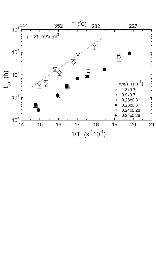
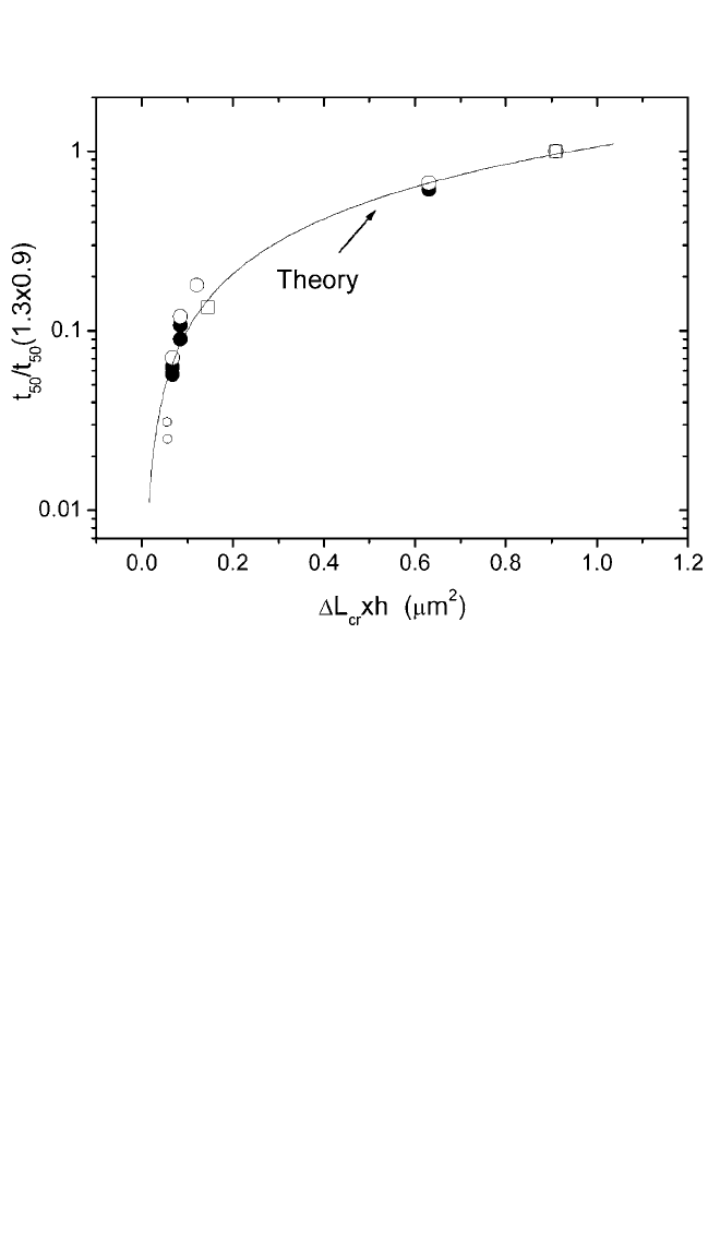
1.3- to 0.24-mm-wide lines, shown in Fig. 9.39, validate the model. In
Fig. 9.40, the relationship between the lifetime ratio of t
50
(w) to t
50
at the
1.3-mm-wide and 0.9-mm-thick line is plotted as a function of ∆L
cr
h.
The t
50
clearly decreases with the decrease in the area ∆L
cr
h. The activation
energy for electromigration Q for these electroplated Cu lines appears to be
constant at about 1 eV. The dependencies on interface transport and line
area are consistent with reports of electromigration failure mechanisms in
Cu lines deposited by PVD and chemical vapor deposition techniques.
[26]
9.11.2 Dual-Damascene Line
Let us consider the case of dual-damascene Cu lines and Cu mass
transport occurring primarily at the top-surface interface and not at grain
boundaries nor the Cu/liner interface. If diffusion at the top Cu/silicon
nitride interface is dominant in Cu damascene lines, the lifetimet for a
single Cu damascene line with a blocking boundary is given by Eq. (18).
462 DIFFUSION PROCESSES IN ADVANCED TECHNOLOGICAL MATERIALS
Figure 9.39 Plot of t
50
vs. 1/T with various line areas for Cu.
Chapter-09 11/29/04 6:50 PM Page 462
ELECTROMIGRATION IN CU THIN FILMS, HUETAL. 463
From Sec. 9.11.1, the Cu electromigration lifetime for a single-damascene
line with a fixed line current density, j
Line
, was shown to be proportional to
the via width (∆L
cr
) times the metal line thickness (h). When ∆L
cr
and h
are scaled down in each new generation, the prediction of Eq. (18) for Cu
electromigration lifetime will be reduced. The trend can be reversed, if we
could modify parameters in Eq. (18), such as the via size (∆L
cr
), metal
thickness, and, especially, interface diffusivity (D
s
).
For Cu dual-damascene lines connected to W underlying lines, multi-
ple failure modes are shown in Sec. 9.7.2. This behavior was found to cor-
relate to the variations of void location where voids are formed in the line
and/or the bottom of the via. Void growth was also attributed to Cu atom
diffusion along the fast diffusion path, the CuSiN
x
interface in these sam-
ples. The drift of Cu atoms along the CuSiN
x
interface at the cathode end
of the line by an electron current generates excess vacancies and con-
comitantly a high tensile stress. The forces from the large vacancy con-
centration and stress gradients generate the vacancy flux. These excess
vacancies easily migrate through the Cu bulk, because of their low migra-
tion energy, and flow to relieve the stress gradient to vacancy sinks, such
Figure 9.40 Normalized lifetimes: t
50
t
50
(1.3 0.9 mm
2
) as a function of line area
estimated from data in Fig. 9.39.
Chapter-09 11/29/04 6:50 PM Page 463

as via bottoms, interfaces, grain boundaries, or the ends of the lines, where
voids may be formed. The short-lifetime group, for example, is found to
result from void growth at the via bottom. The initial Cu line/via stress
generated from the thermal expansion mismatch between Cu and its sur-
rounding materials and the grain orientation near or at the cathode end of
the line/via may play an important role in determining the direction and
accumulation sites of the vacancy wind. The anisotropic variation in
mechanical properties for Cu may have a large effect. The value of
Young’s modulus for copper in the 111 direction is 2.9 times higher
than that in the 100 direction;
[121]
thus a mixture of 111 and
100 orientated grains at the cathode end of the line/via will generate
higher local stress gradients as well as higher overall stress than would be
generated by all 100 orientated grains.
The early failure mode determines the electromigration lifetime of the
IC chips. Thus it is important to know the relationships among via size,
linewidth, and thickness in the scaling rule of dual-damascene Cu inter-
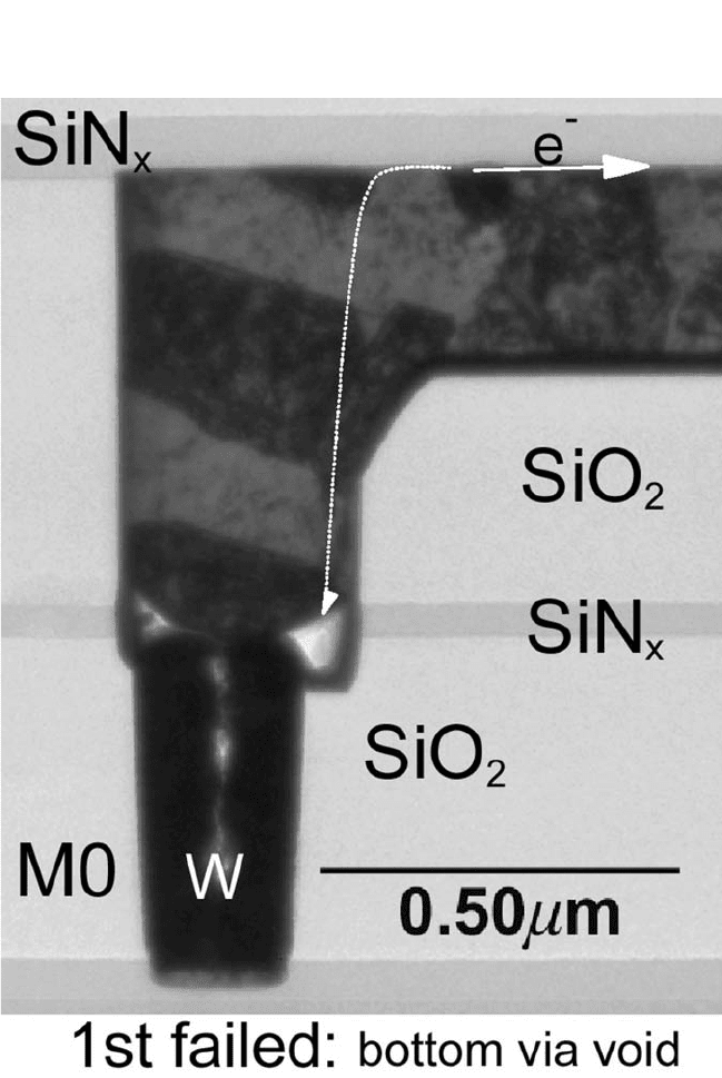
connections. The via bottom void results from the collection of vacancies
produced by electromigration at the top CuSiN
x
interface, as shown in
Fig. 9.41. This TEM image shows the via bottom void at a Cu via and W
interface. Since the electromigration flux is constrained to the top inter-
face within an area of d
s
w, the electromigration lifetime of the via bottom
void, the first lifetime group,can be written as:
t
via
(A
via
∆L
via
) kT(d
s
wD
s
j
Line
eZ
*
r) (20a)
or
t
via
(h∆L
via
) kT(d
s
D
s
j
via
eZ
*
r). (20b)
Here A
via
and ∆L
via
are the area of the bottom via and the critical void
height that causes failure, respectively; j
via
is the current density at the via
bottom; and j
Line
is the current density in the line. Equations (20a) and
(20b) show that the scaling of lifetime for via bottom voids in a dual-
damascene line on a Cu blocking boundary is controlled by either j
via
or
A
via
w for a constant line current density. They show that lifetime
decreases as the linewidth increases for constant j
Line
and constant A
via
.
Figure 9.42(a) and (b) shows the lifetime cumulative probability
plot for dual-damascene 0.27- and 0.90-mm-wide Cu lines stressed at a
sample temperature of 296°C and currents of 2 and 3.2 mA, respec-
tively, using the test structure shown in Fig. 9.3(c). In this case, both
lines are connected to a single Cu via, 0.32 mm in diameter, and a W
underlying line. The cumulative percentage failure distribution is fitted
to a bimodal function. The median lifetimes of the first-failure group (t
1
)
464 DIFFUSION PROCESSES IN ADVANCED TECHNOLOGICAL MATERIALS
Chapter-09 11/29/04 6:50 PM Page 464
ELECTROMIGRATION IN CU THIN FILMS, HUETAL. 465
Figure 9.41 Cross-section TEM image of the first failed sample showing the via
bottom voids. The dotted line shows the possible direction of excess vacancy
flow. The solid line arrow shows the direction of biased mass motion and elec-
tron flow.
Chapter-09 11/29/04 6:50 PM Page 465
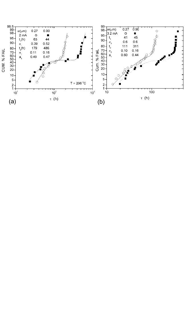
corresponding to void formation at the via bottom (see Fig. 9.43) are 63
and 44 hours with 2 mA, and 41 and 45 hours with 3.2 mA, for 0.27- and
0.9-mm-wide lines, respectively. Since A
via
andwj
Line
are the same for
both linewidths, and both linewidths have similar t
1
, Eq. (19a) is veri-
fied. The second lifetime group (t
2
) was caused by voids formed in both
the line and via or in the line only. The lifetimes of 486 and 311 hours
were obtained from the 0.9-mm-wide lines for 2 and 3.2 mA, respec-
tively, and 179 and 111 hours from the 0.27-mm-wide lines for 2 and
3.2 mA, respectively. The three times longer median lifetime in the second
lifetime group for the 0.90-mm-wide lines compared to the 0.27-mm-
wide lines is due to a lower line current density (3.3 times lower) in the
wide lines, as in Eq. (18), and the slight variation in line shape above a
single Cu via.
Figure 9.43(a) and (b) shows the FIB images from the tested lines in
the first lifetime group for 0.27- and 0.9-mm-wide lines, respectively,
taken at an ion beam angle of 45 degrees. The samples were sectioned
using FIB along the line in (a) and across the lines in (b), respectively.
Similar void sizes and shapes were observed for both linewidths.
Although the current density in a 0.9-mm-wide line is about one-third of
the value of a 0.27-mm-wide line, the fluxes at the top surface and void
size at the via bottom are about the same, which resulted in similar life-
times, as predicted by Eq. (19).
466 DIFFUSION PROCESSES IN ADVANCED TECHNOLOGICAL MATERIALS
Figure 9.42 Cumulative percentage failure of 0.27- and 0.90-mm-wide dual-
damascene Cu lines on W. Both lines are connected to a single via, 0.32 mm in
diameter. The dual-damascence lines were tested with (a) 2 and (b) 3.2 mA at
296°C. Solid and dotted curves are the best fits of the data to a bimodal function.
The parameters t
1
, s
1
and t
2
, s
2
are the median time to failure and the deviation
for the first and second log-normal distribution function, respectively; a
1
is the
amplitude of the first log-normal function.
Chapter-09 11/29/04 6:51 PM Page 466
ELECTROMIGRATION IN CU THIN FILMS, HUETAL. 467
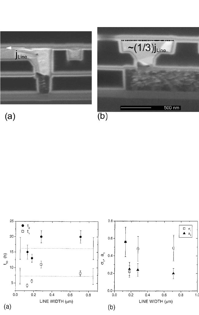
To further validate the proposed model, electromigration in Cu dual-
damascene lines on W in SiLK dielectric with various linewidths and via
bars was investigated. Figure 9.44(a) and (b) shows no large variation in the
values of t
1
, t
2
, s
1
, and a
1
for metal linewidths from 0.13 to 0.73 mm, even
with constant j
Line
, when the via bottom areas are roughly scaled with metal
linewidths. These results are in agreement with the prediction of Eq. (19b).
Figure 9.43 FIB images of early failure mode samples tested at 298°C. (a) Metal
linewidth of 0.24 mm; the arrow shows the direction of electron flow from right to
left. (b) Metal linewidth of 0.9 mm; the circles show the directions of electron flow
into the paper.
Figure 9.44 Plots of the dependence of linewidth on (a) median lifetime of the first,
t
1
, and second, t
2
, and (b) s
1
and a
1
fitting parameters from failure time bimodal
distribution functions of samples stressed with a via bar structure. A constant line
current density was applied.
Chapter-09 11/29/04 6:51 PM Page 467

468 DIFFUSION PROCESSES IN ADVANCED TECHNOLOGICAL MATERIALS
The bottom via areas estimated from FIB images are 0.13 0.12, 0.18 0.18,
0.25 0.20, and 0.65 0.23 mm
2
for 0.13-, 0.18-, 0.28-, and 0.73-mm-wide
lines, respectively. The variations in the values of t
1
are partly due to
the variations of the bottom via current densities, statistical error, and error
generated when measuring the via bottom Cu areas. Also, in this sample set,
error could have been generated by the lithography resolution when
attempting to pattern sub-0.18-mm-wide lines. The current density j
Line
in the
lines was 30 mAmm
2
, while via bottom current densities j
via
were estimated
to be 77, 62, 60, and 50 mAmm
2
for 0.13-, 0.18-, 0.28-, and 0.73-mm-wide
lines, respectively. The dotted lines are the mean values of t
1
and t
2
together
with their uncertainties. Comparing the data obtained from Fig. 9.42 and
Fig. 9.44(b), a slightly lower value of a
1
in CuSilK (0.2) than in CuSiO
2
(0.5) was obtained, which may be attributed to the different thermal expan-
sion mismatch between CuSiLK and CuSiO
2
. Figure 9.45(a) is a FIB
image of a tested sample in the first-failure group with a 0.13-mm-wide line.
Figure 9.45(b) and (c) shows serial images of the t
1
group from a 0.73-mm-
wide line taken 0.3 mm apart. In all three images, voids are observed at the
bottom of the Cu via, although via bottom voids are reduced in the CuSilK
dielectric compared to those in CuSiO
2
structures.
The electromigration lifetime of a dual-damascene line connected to
a completely blocking boundary W line with various Cu via sizes and
linewidths can be reasonably represented by a bimodal function. The
dominant Cu mass motion is along the Cu/dielectric interface. The first-
failure group had void formation at the via bottom and was found to be a
function of metal line thickness divided by the current density at the bot-
tom of the via or bottom via area divided by linewidth. The results from
stressing 0.13- to 0.90-mm-wide dual-damascene Cu lines are consistent
with our proposed model and suggest the importance of the via size used
in Cu interconnections, especially in wide lines.
9.12 Short-Length Effect
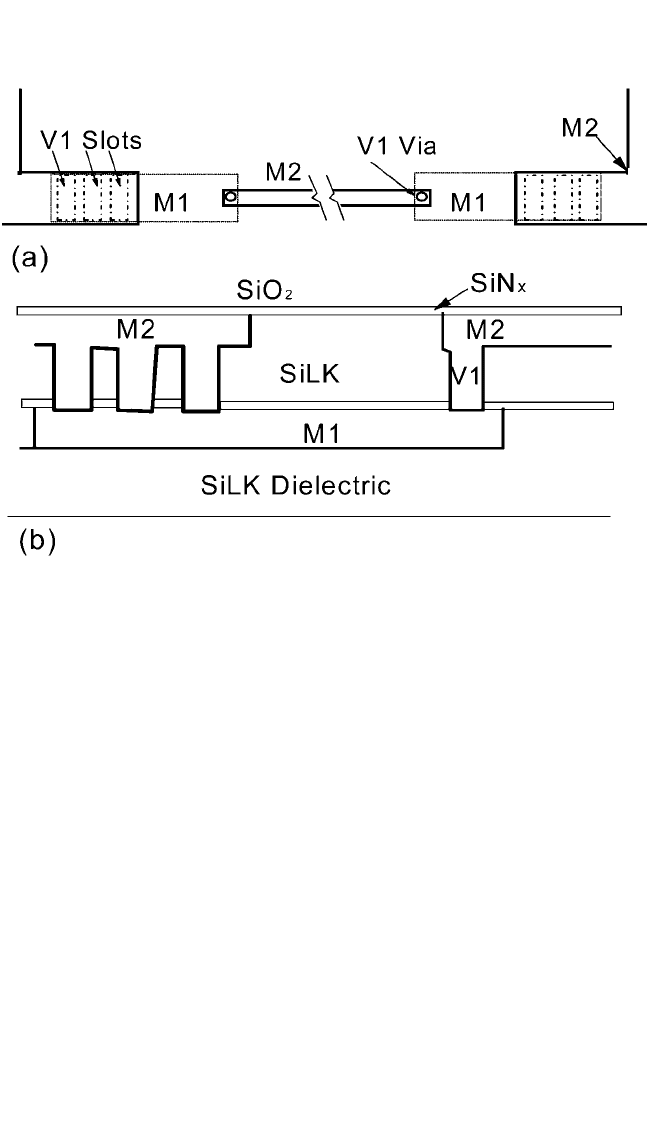
Atwo-level Cu interconnect structure, M1V1M2, was used for this
study.
[122]
Figure 9.46(a) and (b) shows the schematic diagrams of the test
structure. The thicknesses of M1 and M2 are 0.31 and 0.35 mm, respec-
tively. M1 is 3 mm wide and 12 mm long. M2 consists of one 0.21-mm-
wide fine test line and two 3-mm-wide lines on either side of the test line.
The fine M2 is 375 mm long. Each end of the 0.21-mm-wide M2 connects
to one end of the M1 through a V1 via. The top and bottom diameters of
the V1 via are 0.35 and 0.2 mm, respectively. The other end of the M1 is
connected to the 3-mm-wide M2 using three 3-mm-long V1 slots. The
widths of the top and bottom V1 slots are 0.46 and 0.2 mm, respectively.
The Cu M2 was passivated with SiN
x
SiO
2
. A dc current of 1.6 mA was
Chapter-09 11/29/04 6:51 PM Page 468
applied in the test lines, which resulted in current densities, j, in the 0.21-mm-
wide fine M2, 3-mm-wide M2 and M1 of 22, 2.3, and 2.6 mAmm
2
,
respectively. The samples were run at a temperature range from 253 to
365°C. All the electromigration tests were run in a vacuum furnace with
ELECTROMIGRATION IN CU THIN FILMS, HUETAL. 469
Figure 9.45 FIB images of the failed samples tested at 298°C, taken at an ion
beam angle of 45 degrees, for metal linewidths of (a) 0.13 mm;(b) and (c) 0.73 mm.
Voids located at the bottom of vias are shown.
Chapter-09 11/29/04 6:51 PM Page 469
an atmosphere of 10 to 30 torr of forming gas (N
2
-5% H
2
). The average
grain sizes were found to be roughly about 0.7 and 1.4 mm for the 0.21 and
3-mm-wide lines, respectively. The liner thicknesses at the M1V1 via
and M1V1 slot interfaces were measured from TEM micrographs to be
8 and 19 nm, respectively. The variation in the liner thickness is due to the
variation of the PVD step coverage in the various structures.
If the liner at the via/line interface provided complete blocking
boundaries for the Cu fluxes, the void growth rate would be the same as
the drift velocity, since the Cu atoms would drift away from the liner at
the contact interface (the cathode end of the line), creating a void. The Cu
would then drift to the liner at the anode end of the line, generating an
extrusion. The lifetime t is obtained by ∆L
f
t
0
n
d
dt, where t is the
amount of time required to grow a critical void size ∆L
cr
necessary for
∆RR
o
2%.
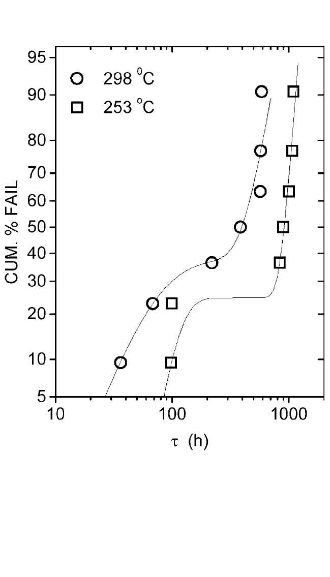
In the case of partial blocking boundaries, voids and extrusions in
metal lines occurred when there was an imbalance of Cu fluxes at a par-
ticular location, x, given by Eq. (10). Figure 9.47 presents data for cumu-
lative percent failure vs. lifetime. It shows two distinguishable groups of
failure times (short- and long-lifetime groups) that cannot be fit by a
470 DIFFUSION PROCESSES IN ADVANCED TECHNOLOGICAL MATERIALS
Figure 9.46 Schematic diagrams of the test structure. (a) Top view; (b) cross-
section view of one side of the test structure.
Chapter-09 11/29/04 6:51 PM Page 470
ELECTROMIGRATION IN CU THIN FILMS, HUETAL. 471
single log-normal distribution. This is similar to the case of CuSiO
2
. A
bimodal distribution function was used. The median lifetime of the short-
lifetime group was about an order of magnitude less than that of the long-
lifetime group. The samples were examined in a FIB microscope to
understand the correlation between void growth, open failure, and lifetime.
Figure 9.47 Plot of cumulative percentage failure vs. lifetime t. Solid lines are the
least-squares fits to the bimodal functions.
Chapter-09 11/29/04 6:51 PM Page 471