Ghodssi R., Lin P., MEMS Materials and Processes Handbook
Подождите немного. Документ загружается.

164 D.P. Arnold et al.
3.3.2.1 Nickel
Electroless nickel plating is one of the most popular catalytic electroless processes
in use today. It is commonly used in engineering coating applications for wear resis-
tance, hardness, and corrosion protection. It is also used in the electronics industry
on PCBs as a coating with an overlay of gold to prevent corrosion. The concept and
basic composition has not changed much since the inception of the process [58]. The
electroless nickel plating bath consists of a source of nickel ions (salts), a reducing
agent, complexing agents, and some additives.
Although many nickel salts such as nickel sulfate, nickel chloride, and nickel
acetate are available, nickel sulfate is preferred because of its low corrosiveness
and low cost. To enhance chemical reduction of nickel at the cathode, a reducing
agent is used such as sodium hypophosphite (NaH
2
PO
2
H
2
O), sodium borohydride
(NaBH
4
), and dimethylamine borane (DMAB). Complexing agents are used for
exerting a buffering action to prevent the pH change, preventing the precipitation
of nickel salts, and enhancing stable metal reduction. Note that because there are
several agents inserted in the bath, nickel from electroless plating is not usually
pure but contains other components such as phosphorus or boron.
Table 3.9 shows some bath compositions for electroless nickel deposition with
hypophosphite reducing agent (columns 1–4), borohydride r educing agent (columns
5–6), and dimethylamine borane reducing agent (columns 7–8) [61].
A step-by-step procedure for nickel electroless plating with a hypophosphite
reducing agent is given below and in Table 3.10 [9, 62], which essentially follows
the r ecipe of Table 3.9 (column 1) except for the amount of hydroxyacetic acid of
30.9 g/L and the process temperature of 65
◦
C. With this recipe, a deposition rate
of approximately 70 nm/min (4.2 μm/h) is obtained on a printed circuit board and
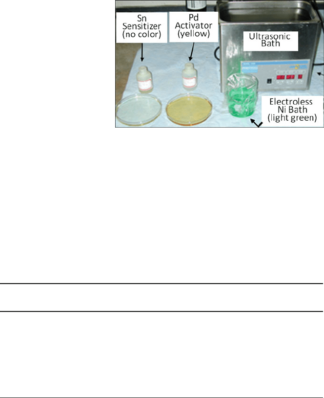
a Si substrate. The equipment necessary for electroless nickel plating is shown in
Fig. 3.14, consisting of an Sn sensitizing bath, a Pd activation bath, an electroless
nickel bath, and an ultrasonic bath.
Bath Preparation
1. Mix 10 g of SnCl
2
and 10 g of HCl. Take 0.375 mL of the solution and mix it
with 120 mL of deionized water to prepare the Sn(II) solution.
2. Mix 10 g of Pd and 10 g of HCl. Take 0.5 mL of the solution and mix it with 100
mL of deionized water to prepare the Pd(II) solution.
3. Measure 129.62 g NiCl
2
, 105.97 g NaH
2
PO
2
·H
2
O, and 61.8 g HOCH
2
COOH
into a 1 L beaker. Fill the beaker with deionized water to 1 L. Mix using a motor-
ized mechanical propeller for at least 2 h. (Note that a magnetic stirring bar is not
recommended because the bath contains ferromagnetic Ni.) This stock solution
can be stored for a month or two without noticeable degradation.
4. Add NH
4
OH to obtain a pH level of 4–6. Mix well for 2 h in a similar way to that
described above. This pH adjustment should be performed immediately before
performing electroless plating.

3 Additive Processes for Metals 165
Table 3.9 Example baths for electroless nickel deposition using various hypophosphite reducing agents
Hypophosphite reducing agent
Borohydride reducing
agent
Dimethylamine borane
reducing agent
Bathconstituentsandparameters 12345678
Nickel chloride (NiCl
2
·6H
2
O)(g/L) 303030 2024170
Nickel sulfate
(NiSO
4
·6H
2
O) (g/L)
25 30
Sodium hypophosphite (NaH
2
PO
2
·H
2
O) (g/L) 10 10 10 25
Hydroxyacetic acid (HOCH
2
COOH) (g/L) 35
Sodium citrate (Na
3
C
6
H
5
O
7
·2H
2
O) (g/L) 12.6 84
Sodium acetate (NaC
2
H
3
O
2
)(g/L) 5
Sodium borohydride (NaBH
4
) (g/L) 0.67 0.4
Ethylenediamine (C
2
H
4
(NH
2
)
2
) (g/L) 44
Sodium hydroxide (NaOH) (g/L) 40
Ammonium hydroxide (NH
4
OH, 28% NH
3
) (mL/L) 120
Dimethylamine borane ((CH
3
)
2
NHBH
3
)(g/L) 37 3.5
Malonic acid (C
3
H
2
O
4
Na
2
, disodium salt) (g/L) 34
Ammonium chloride (NH
4
Cl) (g/L) 50
Boric acid (H
3
BO) (g/L) 25
Sodium pyrophosphate (Na
4
P
2
O
7
·10H
2
O) (g/L) 50
Base for neutralizing NaOH NaOH NH
4
OH NH
4
OH NaOH NH
4
OH NaOH NH
4
OH
pH 4–6 4–6 8–10 10–11 11 11 4.25 5.5
Temperature (
◦
C) 90–100 90–100 95 70 97 60 18 77
Deposition rate (μm/h) 15 7 6.5 15 8.8 1.3 2.3 21
References [62][63][58][64][65][65][66][67]

166 D.P. Arnold et al.
Fig. 3.14 Preparation of
electroless nickel plating
Electroless Nickel Plating Procedure
1. Rinse a substrate in acetone, then methanol, then deionized water, and then
sensitize it in the Sn(II) solution for 2 min.
2. Rinse the sample in deionized water for 30 s.
3. Catalyze the sample in the prepared Pd(II) solution for 2 min.
4. Rinse the sample in deionized water for 30 s.
5. Submerge the sample in the prepared electroplating bath at 65
◦
C in an ultrasonic
environment.
Table 3.10 Ingredients of electroless nickel bath with hypophosphite reducing agent [9]
Bath constituents and parameters Molarity (mol)
Molecular
weight Mass (g/L)
Nickel chloride
(NiCl
2
·6H
2
O)
0.23 129.62 30
Sodium hypophosphate
(NaH
2
PO
2
·H
2
O)
0.09 105.97 10
Hydroxyacetic acid
(HOCH
2
COOH)
0.5 61.8 30.90
pH 4–6 (using NH
4
OH or NaOH for adjustment)
Temperature 65
◦
C
3.3.2.2 Copper
Some electroless copper plating recipes use formaldehyde or its derivatives as a
reducing agent. However, such plating baths produce toxic f ormaldehyde vapor dur-
ing the process and require high pH (~12.5). An alternative bath uses hypophosphite
as the reducing agent. Table 3.11 shows some bath compositions for electroless cop-
per deposition with formaldehyde reducing agent (columns 1–3) and hypophosphite
reducing agent (column 4) [61, 68].

3 Additive Processes for Metals 167
Table 3.11 Example baths for electroless copper deposition using formaldehyde reducing agent
and hypophosphite reducing agent
Formaldehyde reducing
agent
Hypophosphite
reducing agent
Bathconstituentsandparameters 1234
Copper sulfate (CuSO
4
·5H
2
O) (g/L) 3.6 30 10 3.83
Nickel sulfate (NiSO
4
·6H
2
O) (g/L) 0.53
Boric acid (H
3
BO
3
) (g/L) 30.9
Sodium hypophosphite (NaH
2
PO
2
·H
2
O) (g/L) 28.6
Sodium potassium tartrate (KNaC
4
H
4
O
6
·4H
2
O)
(g/L)
25 99
Sodium hydroxide (NaOH) (g/L) 3.8 50 10
Sodium carbonate (Na
2
CO
3
) (g/L) 32
Formaldehyde (HCOOH (37%)) (g/L) 10 29 20.3
Sodium citrate (Na
3
C
6
H
5
O
7
·2H
2
O) (g/L) 15.3
Methyldichlorosilane (CH
3
Cl
2
SiH) (g/L) 0.25
Ethylenediaminetetraacetic acid (EDTA)
tetrasodium (N,N
-1,2-
Ethanediylbis[N-(carboxymethyl)glycene]
tetrasodium) (g/L)
20
Temperature (
◦
C) 22 25 63 65
Deposition rate (μm/h) 0.5 2.5 6.3 8.5
References [69][70][71][68]
The hypophosphite reduced electroless copper plating has advantages including
bath stability, no toxic gas generation, and operation in a lower pH environment.
However, because the deposited copper cannot catalyze the oxidation of hypophos-
phite, the bath needs a small amount of nickel for continuous plating and boric acid
for a high plating rate, resulting in impure copper deposition.
A step-by-step procedure for copper electroless plating with a hypophosphite
reducing agent [68] is given below as an example.
Bath Preparation
1. Mix 10 g of SnCl
2
and 10 g of HCl. Take 0.375 mL of the solution and mix it
with 120 mL of deionized water to prepare the Sn(II) solution.
2. Mix 10 g of Pd and 10 g of HCl. Take 0.5 mL of the solution and mix it with 100
mL of deionized water to prepare the Pd(II) solution.
3. Mix the electroless copper plating bath with hypophosphite reducing agent
following Table 3.11 (column 4).
4. Adjust the pH with either KOH or NaOH pellets to the desired pH level (Here it
is 9–9.5).
Note that all ingredients are mixed and dissolved in water together. The mixture
after step 3 can have a shelf life of about a month, but the mixture after step 4 tends

168 D.P. Arnold et al.
to plate a thin copper layer on the container wall in a few days. The pH adjustment
should be done right before electroless plating is performed. The solution should
have a clean blue color.
Electroless Copper Plating Procedure
1. Rinse substrate in acetone, then methanol, and then deionized water, and then
sensitize it in the prepared Sn(II) solution for 2 min.
2. Rinse the substrate in deionized water for 30 s.
3. Catalyze the substrate in the prepared Pd(II) solution for 2 min.
4. Rinse the substrate in deionized water for 30 s.
5. Submerge the substrate in the prepared electroless plating bath.
3.3.2.3 Gold
Because of its high chemical stability and mechanical ductility, gold becomes an
indispensable material in the electronics industry. Despite its importance, electro-
less gold plating [29] has been underdeveloped compared with electroless nickel or
copper. Useful electroless gold plating using borohydride or amine borane as the
reducing agent has been reported [72, 73]. A typical bath composition is shown in
Table 3.12.
Table 3.12 Ingredients of electroless gold bath with borohydride reducing agent [73]
Bath constituents and parameters Molarity (mol) Molecular weight Mass (g/L)
Potassium gold cyanide
(KAu(CN)
2
)
0.02 290 5.8
Potassium cyanide (KCN) 0.2 65 13
Potassium hydroxide (KOH) 0.2 56 11.2
Potassium borohydride (KBH
4
) 0.4 54 21.6
Temperature 75
◦
C
Deposition rate 0.7–3.5 μm/h (with stirring)
Bath Preparation (2.5× Concentration) [67]
1. Dissolve 28 g KOH and 32.5 g KCN in about 500 mL of deionized water.
2. Add54gKBH
4
and stir until dissolution.
3. Dissolve 14.4 g KAu(CN)
2
in about 250 mL deionized water.
4. Mix the above two solutions, and dilute to 1 L.
5. Filter through Whatman 41 filter paper or equivalent.
6. Dilute 1 volume of this solution with 1.5 volumes of deionized water to make a
2.5× bath.

3 Additive Processes for Metals 169
3.3.3 Comparison of Electroplating and Electroless Plating
Ni, Cu, and Au microstructures can all be fabricated by electroplating or electro-
less plating. Compared to electroplating, electroless plating contains the following
characteristics and advantages [61].
1. No power supply and electrical contact is necessary.
2. Deposition may occur on a nonconducting surface.
3. More uniform deposition can be formed on three-dimensional geometry without
electric field influence.
4. Deposits are often less porous.
There are disadvantages of electroless plating too. Often the electroless baths
require higher temperatures and have a relatively short lifetime. Electroless plating
is also prone to poor adhesion. Care should be taken when storing electroless plating
baths. A container made of plastic or glass is often found to be covered with elec-
troless plated metal after being stored on the shelf for a while. Also, for electroless
plating, the deposition rate is relatively slow, and metal layers thicker than a few
micrometers are not recommended. In addition, electroless plating metal in selected
regions can sometimes be quite challenging. For example, selective deposition on
a metal surface is fairly easy, but selective coating a polymer on SiO
2
is not very
effective (the bath will likely deposit on both the polymer and SiO
2
surfaces).
Costs of electroplating and electroless plating are fairly similar. The electroless
plating process requires a chemical reducing agent for metal ions to be converted
into the elemental conformation, therefore it is considered as a more expensive pro-
cess from the material cost point of view. However, this chemical cost is offset by the
advantage of not requiring equipment such as power supplies or switching circuits
for advanced current control.
There are clearly pros and cons associated with both electroplating and electro-
less plating. In situations where either electroplating or electroless plating could
theoretically be used, the decision for one or the other is often dependent on many
process integration issues. In general, electroless plating can be considered as a
complement to electroplating rather than a “competitor.”
3.4 LIGA and UV-LIGA Processes
One of the most distinctive MEMS processes is the construction of thick and high-
aspect-ratio three-dimensional (3-D) microstructures. High aspect ratio is modestly
defined as a height to width ratio of 2 to 1 or greater. Fabrication of these structures
often relies on X-ray or UV lithography of thick polymer layers.
4
The patterned
4
See Chapter 9 for m ore information on lithography.

170 D.P. Arnold et al.
polymeric structures can be used directly as a MEMS device or used as a mold for
metal electrodeposition. In this section, two fabrication approaches for achieving
high-aspect-ratio 3-D electroformed metallic structures are described: one with X-
ray lithography (LIGA), and the other with UV lithography (UV-LIGA or LIGA-
Like).
5
3.4.1 Process Explanation
Both LIGA and UV-LIGA processes share common fabrication steps except for the
initial step of polymeric mold fabrication. A general fabrication procedure for both
processes is described in this section.
Because these are surface micromachining processes, there is no strict crite-
rion for substrate selection. A variety of substrates such as Si, glass, ceramic, and
printed wiring board are available, however, an oxidized Si substrate is used as an
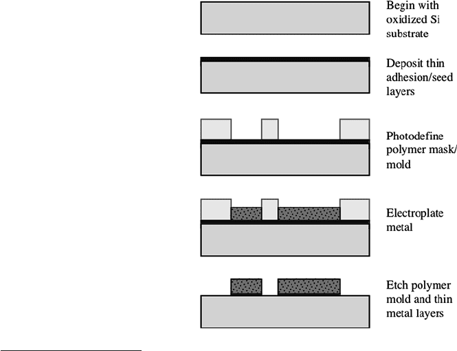
example here ( Fig. 3.15). An electrical seed layer typically consisting of Ti/Cu or
Cr/Cu is deposited on the substrate using either sputtering or evaporation. Cu does
Fig. 3.15 Basic
electroplating process to form
single-layer metal structures
5
The German acronym “LIGA” refers to a three-step process: X-ray-Lithography, Electroplating
(german: Galvanik), Polymer Replication (German: Abformung). Nowadays, “LIGA” is commonly
used in reference to the two-step process of lithography and electroplating (excluding the polymer
replication step).
3 Additive Processes for Metals 171
not stick well to most substrates so Ti or Cr is employed as an adhesion layer
(see Section 3.5.1). Typical thicknesses of Ti (or Cr) and Cu are 10–30 nm and
100–300 nm, respectively. After the seed layer deposition, a thick polymer layer
is coated, soft-baked, and lithographically patterned to form a micromold for a
subsequent electroplating. LIGA typically uses polymethylmethacrylate (PMMA)
or SU-8 (an epoxy-based polymer) for X-ray lithography, whereas UV-LIGA uses
various UV-sensitive photoresists including DNQ-novolak-based photoresist, SU-8,
polyimide, and others.
With the photoresist mold in place, the substrate is then electroplated. The elec-
troplated metal fills the mold confined by the sidewalls. Usually the electroplating
is stopped before it reaches the top of the mold. But sometimes it is electroplated
over the mold to form “mushroom”-type structures for some applications. After
electroplating, the polymer mold is removed using a solvent and/or plasma etching.
The electroplated structures are still electrically connected to each other through the
seed layer. The Cu and Ti seed layers are then sequentially time etched to isolate the
electroplated structures electrically and complete the process.
With the introduction in the 1990s of UV photopatternable high-aspect-ratio
polymers such as SU-8, high-quality sidewall and high-aspect-ratio molds could
be fabricated using UV lithography, as compared to X-ray lithography. The electro-
forming process using UV-patterned molds and subsequent electroplating has been
called UV-LIGA, LIGA-like, or often “poor man’s LIGA.”
The UV-LIGA process does not provide the extreme aspect ratios possible with
X-ray LIGA, but is sufficiently suitable for many applications. A good guideline
is that an aspect ratio of 6:1 can be fabricated by UV-LIGA. It is also restricted
to a maximum resist height of 800 μm or s o. Also submicron pattern dimensions
may not be effectively produced because of the wavelength of the UV source, for
example, i-line (λ = 365 nm). However, in addition to low cost in equipment, the
process has other advantages such as batch processability, manufacturability, and
relative simplicity, providing an affordable system set for laboratory and industrial
usage.
3.4.2 Electroplating in LIGA and UV-LIGA Microstructures
The height and surface profile of high-aspect-ratio electrodeposited metal structures
and the homogeneity of their thickness distribution are influenced by various factors,
which can interfere with each other. The main factors and important effects are
explained in this section.
The deposition rate is proportional to the current density. Therefore a higher cur-
rent density results in a thicker deposit. The distribution of the current density is
associated with the distribution of the electric field lines (primary current distribu-
tion). Because the metal surface is highly conductive, the field lines are normal to
the electrode surface. If the anode has a larger area than the cathode, the field line
density and current density are higher at the edge of the substrate, which causes a

172 D.P. Arnold et al.
thicker deposit at the edge of the s ubstrate (“macro bathtub effect”). I f the cathode
surface is patterned with resist structures, the electric field lines bend, and a current
concentration occurs at the edge of the structures [74, 75]. Therefore the electro-
plated layer is usually thicker near the edges of the electroplated features (“micro
bathtub effect”) and sometimes higher in narrow structures than in wide structures,
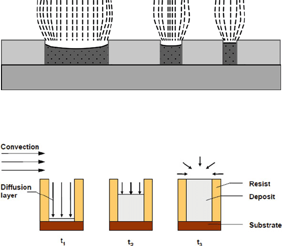
as shown in Fig. 3.16.
Another consideration for electroplating in high-aspect-ratio features is that the
transport mechanism of the metal ions depends on feature size and depth. As a
result, the electroplating rate may vary during the plating process [76]. Figure 3.17
shows three different states that occur in filling a mold structure by electroplating.
At the beginning of the deposition, the process is highly diffusion limited. As the
plated layer grows and the trenches begin to fill, the diffusion limitations begin to
wane. At an intermediate filling, the penetration range of the convection is reached.
This depends on the lateral size of the structure itself. In the case of structures with
sufficiently wide lateral dimensions, the flow velocity in the plating bath reduces the
extension of the diffusion layer, as described in Section 3.3.1.2. Very high-aspect-
ratio structures therefore show a reduced plating rate in the beginning of plating. In
this case, the electroplated layer would be thinner in narrow structures, as compared
to wider structures.
Fig. 3.16 Schematic of electrical field line distribution using resist-patterned substrates. The field
line density is higher within narrow structures and at the edge of wide structures, which affects the
height and surface profile of the electroplated microstructures
Fig. 3.17 Schematic of the diminishing influence of diffusion during metal growth. The diffusion
layer thickness depends on process progress and on the penetration range of convection. At t
3
,the
deposition rate is improved due to spherical diffusion
3 Additive Processes for Metals 173
All these effects cause inhomogeneous deposition rates over t he substrate as well
as within the features. To minimize these unwanted effects and improve the plating
uniformity, some rules are given in the following.
1) Use a shield or a wafer holder to homogenize the electrical field at the
macroscopic scale.
2) Use dummy plating areas over the whole substrate to promote a homogenous
current distribution.
3) Use microstructured dummy areas that surround the functional features.
4) Use moderate flow to get similar heights of diffusion layers.
5) Use moderate current density to avoid insufficient supply of ions at the bottom
of the microstructure.
6) Limit the deposition height to be about 2/3 of the mold height (see Fig. 3.17
for t
2
).
More rules for LIGA design can be found in [77].
To show the potential of the LIGA techniques, one example is given. Figure 3.18
shows (a) a SU-8 resist mold and (b) the replicated Ni–Fe structure. The electroplat-
ing produces the exact negative of the structural details and the sidewall roughness
of the resist mold. In Fig. 3.19 a commercially available micro gear system is
shown. Crucial features for this application are the high aspect ratio in combina-
tion with the parallel sidewalls of the r esist structure, which is typical for LIGA.
Other applications of LIGA are described in [78, 79].
3.4.3 Multilevel Metal Structures
Often multiple metal levels and vias are necessary to enable complex wiring inter-
connections or complex mechanical microstructures. Multilevel fabrication can be
achieved by extending the previously described process (see Section 3.4.1)using
multiple masking and electroplating steps. For wire connections, an interlayer
dielectric material must be selected to electrically insulate the metal layers from
each other to avoid unexpected short circuits. Considering that the top surface of
the first metal layer may be fairly rough (typical of many electroplated metals), the
dielectric must be able to conformally and completely coat the top and side surfaces
of the lower metal layer. Even the smallest pinhole defect in the interlayer dielec-
tric can cause the electrical insulation to fail. Commonly used interlayer dielectric
materials include PECVD or sputtered oxide/nitride, spin-on glass, or a chemically
stable spin-coated polymer such as polyimide or SU-8. The intended temperature of
operation must also be considered, because polymer dielectrics may not be suitable
at a 100
◦
C or more.
A fabrication process for achieving a two-layer metal structure is shown in
Fig. 3.20. The process begins by depositing the first metal l ayer as described in
Fig. 3.15. The interlayer dielectric is deposited and vias are opened to provide
