Ghodssi R., Lin P., MEMS Materials and Processes Handbook
Подождите немного. Документ загружается.

144 D.P. Arnold et al.
transported and deposited on the substrate wafers. The deposition rate is increased
as the sputtering power is increased, however, too much power causes damage on
the substrate. To counteract this effect, magnetron sputtering has been introduced to
increase the deposition rate. A magnet placed behind the target creates a field that
guides electron movement near the target, causing more efficient ionization of Ar
without excessively high voltages.
3.2.2.2 RF Sputtering
As an alternative to the DC supply, RF power systems can be used, as shown in
Fig. 3.2b. The RF sputtering system also requires a DC bias voltage to generate
plasma. After plasma is generated, however, the major driving force acting on the
argon ions is exerted by the alternating current source. Typically the 13.56 MHz
industry, science, and medicine (ISM) frequency band is used. Because alternating
currents can flow across dielectric materials, RF sputtering systems can deposit not
only electrically conducting materials, such as metals, but also dielectric materials,
such as SiO
2
,Si
3
N
4
, and glass, which are not achievable with DC sputtering due to
charging effects. Also, by reversing the electrical connections, the substrate can be
bombarded as opposed to the metal target. This process is often used to clean the
substrate surface before depositing the target material.
3.2.2.3 Step Coverage
In contrast to the evaporation process, sputtering provides reasonably conformal
coatings on uneven surfaces. This is particularly useful for the metallization of three-
dimensional (3-D) MEMS structures as well as the metal interconnect of integrated
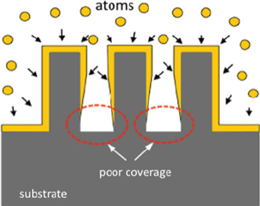
circuits. The step-coverage of a sputtered thin film in a via hole has been calcu-
lated [3, 4], where the profile shows a high deposition rate on the top surface and a
low deposition rate on the sidewall. As a result, the sidewall thickness tapers down
toward the bottom. For a very high aspect ratio, the bottom portion may not have
sufficient metal coverage due to limited mass transfer into the narrow entrance of the
via hole and the higher pressure environment in the chamber. This effect is depicted
in Fig. 3.3. This kind of poor coverage is more significant in high-aspect-ratio vias
or trenches as compared to high-aspect-ratio pillars or walls.
The step coverage can be improved by substrate heating to enhance surface
diffusion or by applying an RF bias to the wafers to introduce surface bombard-
ment resulting in redeposition on the sidewalls [1]. The heating approach may be
applicable to the metal interconnect process for ICs, where the insulating layer
is a temperature-tolerant material such as SiO
2
, however, it may not be directly
applicable for the metallization of 3-D MEMS structures where the structural mate-
rial is often a temperature-intolerant polymer. Step-coverage of thin films for very
high-aspect-ratio MEMS structures remains a challenging area. Alternatively, elec-
troless plating may be used for the thin film metallization of such high-aspect-ratio
polymeric structures.
3 Additive Processes for Metals 145
Fig. 3.3 Sputtered metal
deposition in a densely placed
high-aspect-ratio structure
3.2.2.4 Other Issues in Sputtering
One concern in thin-film deposition using sputtering (or evaporation) on a thick
3-D polymeric layer is that the residual solvent or moisture tends to degas under
high vacuum conditions, resulting in poor adhesion between the polymer and
thin-film metal layer. To prevent degassing effects, an additional hardbake step is
recommended before the sputtering or evaporation process can be used.
One feature found in many sputtering systems is the ability to “clean” the sub-
strate before the metal deposition by sputter etching. This cleaning step can improve
adhesion of the metal. Sputter etching can be implemented either by reversing the
electrical connections or by placing negative bias on the substrate with respect to
the plasma, resulting in increasing ion bombardment on the substrate. Increasing
the incident ion energy increases the adatom (Ar ion) mobility, which can aid in
cleaning the deep sidewalls of a 3-D structure, thereby improving step-coverage
in deep-etched features [5]. However, high sputter etch rates may cause substrate
damage.
Although sputtering of alloy is commonplace, there are several important issues
and approaches. In sputtering, the deposited film composition is usually fairly close
to that of the bulk target, so alloys can be rather easily obtained. However, different
elements in the target alloy may exhibit different sputter yields, causing composi-
tion variation. To achieve better control of stoichiometry, a multiple target system
may be used, where the power of each target can be individually controlled to alter
the final composition of the alloy layer. Also, by using a composite target with dif-
ferent regions of concentration or by changing electrical properties of the plasma,
the composition of the deposited layer can be controlled [6].
Moreover, sputtered compounds can intentionally have a very different com-
position from the sputter target by adding reactive gaseous precursors during the
deposition. Reactive sputtering is a process in which the normally inert sputter gas is
replaced by an inert/reactive mixture [1]. For example, TiN, one of the most popular
diffusion barrier layers in IC fabrication, can be deposited using reactive sputter-
ing. By controlling the partial pressure of nitrogen in the sputtering system, the
composition of TiN can be controlled.
146 D.P. Arnold et al.
Stress is also an important issue for sputtered films. A thin film deposited on a
substrate is subjected to either tensile or compressive stress as influenced by the base
layer and deposition conditions. One component of the stress – known as extrin-
sic stress – is due to thermal expansion mismatch of the film with the substrate.
This stress may be significant if the wafer temperature varies (intentionally or unin-
tentionally) from room temperature during the film deposition. In addition, large
intrinsic stresses may also occur depending on deposition rate, film thickness, and
the background chamber environment. In many cases, efforts are made to minimize
these stresses. Alternatively, for MEMS devices, these stresses can be put to good
use to realize devices such as bimorph actuators or stress-engineered 3-D structures
[7, 8].
3.2.3 Pulsed Laser Deposition
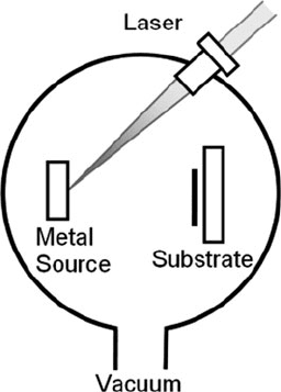
Pulsed laser deposition (PLD) is another method for depositing metals, although
much less often used for MEMS. As shown in Fig. 3.4, the system uses a high-
energy laser beam (typically 10
8
W/cm
2
) to strike a metal target within a vacuum
chamber. The laser beam melts, evaporates, and ionizes a region of the target. This
ablation process creates a vapor plume that transfers material to the sample wafer.
One major advantage of PLD for MEMS applications is precise stoichiome-
try/composition control and relatively fast deposition rates. Ideally the deposited
material possesses the same chemical composition as the metal target. High quality
crystalline deposits are also possible with substrate heating. The biggest drawback
is that most PLD systems can only provide uniform deposition over a small surface
area, sometimes only about one square centimeter. This decreases the utility of PLD
for volume manufacturing. Despite this drawback, PLD finds application where
Fig. 3.4 Schematic of pulsed laser deposition system
3 Additive Processes for Metals 147
precise stoichiometric control is paramount, especially for complex multielement
materials. For metallic systems, this alloy control is beneficial for realizing high-
performance magnetic materials and superconductors. PLD also finds widespread
application for many other complex nonmetallic films, such as oxides, nitrides, and
semiconductors.
The exact process and resulting film composition and structure are dependent on
the laser parameters, chamber pressure/atmosphere, sample temperature, and sam-
ple surface quality. The complex physical and chemical interactions are the subject
of ongoing research.
3.3 Electrochemical Deposition
Electrochemical deposition involves the reduction of metal ions from aqueous,
organic, or fused-salt electrolytes. The reduction of metal ions M
z+
in aqueous
solution is represented by
M
z+
(metal ion in solution) + ze
−
(electrons) → M (metal deposit)
Two processes can be used to provide the electrons for the reduction reaction:
(1) electroplating (or electrodeposition), where an external power supply provides
the electrons, or (2) electroless deposition, where a reducing agent provides the
electrons.
In MEMS electrochemical deposition is commonly used to deposit surface
coatings, or in the case of electroforming, for producing an entire microstructure
or device. In electroforming, microstructured molds of different materials (e.g.,
polymers/resist, silicon) are electrochemically filled with metals such as nickel,
copper, gold, or various metal alloys. More details can be found in Section 3.4.
3.3.1 Electroplating
The material properties of electroplated metals or alloys are strongly influenced
by the chemistry of the electrolyte (e.g., type and concentration of ions, pH, type
of additives), the physical parameters of the process (e.g., temperature, fluidics,
current), and the property of the substrate (surface quality, shape). Depending on
the metal to be plated and/or on the shape of the desired microstructures, the
electroplating process has to be adapted to the specific application. The basics of
electrochemical deposition can be found in several excellent books (e.g., [9–11])
and are summarized in this section. In addition, starting recipes are provided for
some of the most common electroplated metals for MEMS: nickel, copper, gold,
and some nickel alloys.
3.3.1.1 Electrochemical Reactions
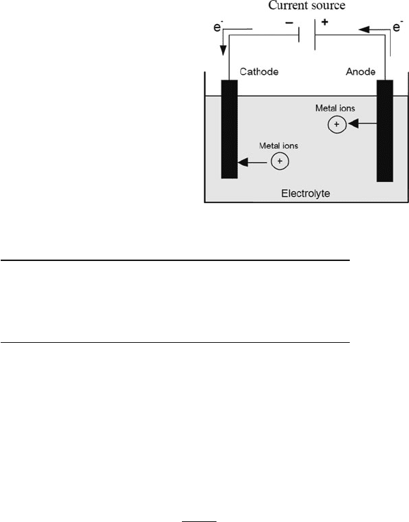
The general setup and operation of an electrochemical deposition cell are shown in
Fig. 3.5. Two electrodes are immersed into an electrolyte. By applying an electric
148 D.P. Arnold et al.
current, reduction (electron uptake) takes place at the cathode, and oxidation (elec-
tron liberation) occurs at the anode. In the case of electroplating, the substrate serves
as the cathode, and metal ions are reduced to form a solid lattice. The anode can be
soluble, meaning it is dissolved via oxidation during the electroplating process. The
two partial reactions are expressed by the following equations.
Fig. 3.5 Schematic of a
general electrochemical
deposition cell (using soluble
anode)
Reduction (cathode): M
z+
+ ze
−
→ M
Deposition of metal
Oxidation (anode): M → M
z+
+ ze
−
Dissolution of metal (for a soluble
anode)
The steady oxidation of the anode (a metal to be deposited) ensures a constant
replenishment of metal ions in the electrolyte. Sometimes inert anodes such as plat-
inum are used, for example, in gold electroplating. In this case, replenishment of
metallic ions in the electrolyte is solely provided by manual addition of metal salts
to the plating bath.
The theoretically deposited mass m
theo
can be calculated from the electrochemi-
cal Faraday’s law as
m
theo
=
M
∗
I
∗
t
z
∗
F
(3.1)
where M = Molar mass the deposited metal; I = Current; t = Time; z =
Valency; F = Faraday constant.
Other reactions also can occur due to decomposition of water. By the oxidation of
water, oxygen gas can be produced at the anode. By the reduction of water, hydrogen
gas can be released at the cathode. Other components of the electrolyte can also react
at the electrodes. The overall current is thus distributed to these different reactions.

3 Additive Processes for Metals 149
The percentage of the total current associated with the reduction of metal is defined
as the cathodic current efficiency γ and can be calculated by the quotient of the
effective deposited mass m
eff
and the theoretical deposited mass m
theo
,
γ =
m
eff
m
theo
. (3.2)
If hydrogen production at the cathode cannot be suppressed, it usually severely
reduces the current efficiency of t he deposition process. Another adverse effect is the
rise of the pH at the electrode surface, which leads to the buildup and incorporation
of metal hydroxides into the deposits, leading to a brittle deposit. The accumula-
tion of hydrogen bubbles, which adhere on the surface, can also cause pores in the
deposit.
3.3.1.2 Deposition Process
In the bulk electrolyte, cations are enclosed in a complex shell. This complex shell
consists of water molecules (hydration shell) or other complexing agents such as
sulfite or cyanide. Before applying a current, the ion concentration is homogeneous
at the electrode surface and in the bulk solution. When applying a current, the metal
ion is consumed at the electrode, and this depletion region extends farther away into
the bulk as the deposition proceeds.
Movement of the complexed metal ions in the electrolyte is governed by three
different mass transport mechanisms: migration, convection, and diffusion. In most
deposition processes the conductivity of the electrolyte is relatively high, and the
applied potentials are moderate. As a consequence, most of the electrical field
drops across the electrical double layer in front of the electrodes, and field-induced
migration is minimal. Therefore the predominant transport mechanisms are usually
convection (due to stirring or agitation), which dominates in the bulk electrolyte,
and diffusion, which dominates near the surface of the electrodes.
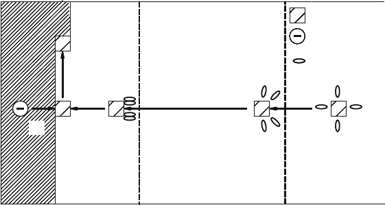
The reduction of the metal ions at the cathode is very complex and can be divided
into four parts: (1) diffusion of the solvated or complexed metal ions from the
bulk solution to the electrode surface, (2) dehydration and transport of the cations
through the electric double layer, (3) cationic reaction at the solution–solid inter-
face (ion uptake and electron transfer), and (4) surface migration and incorporation
of the adsorbed metal atoms into the metal lattice. Figure 3.6 depicts the overall
process.
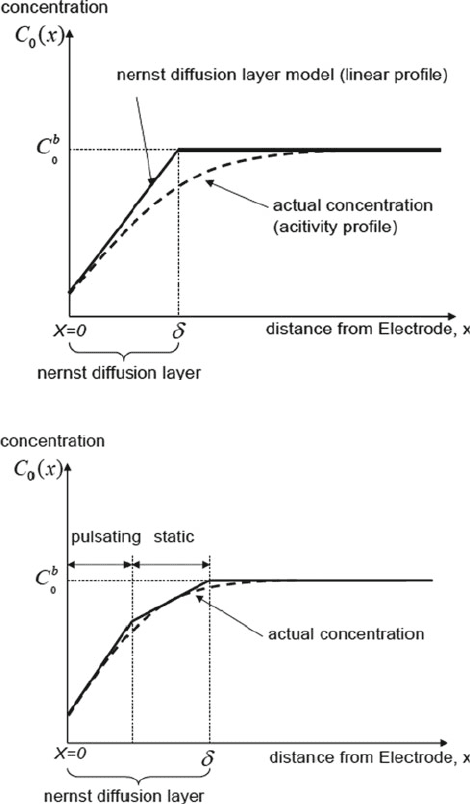
The ion diffusion is described as follows. The region immediately next to the
cathode is characterized by a fictitious Nernst diffusion layer, where the gradient
of ion concentration is assumed constant, as shown in Fig. 3.7. The thickness of
this layer δ is strongly influenced by convection (agitation) in the electrolyte, but
is typically on the order of tens to hundreds of micrometers. In stirred electrolytes
the thickness of the diff usion layer will be determined by this forced convection,
whereas in unstirred electrolyte baths the diffusion layer increases with time.
150 D.P. Arnold et al.
bulk solution
+++
diffusion layerelectric
double layer
cathode
(1)(2)
(4)
electron
+
cation
+++
water molecule
or complexing agent
+++
(3)
Fig. 3.6 Schematic diagram of the electrochemical deposition process
The deposition rate can be enhanced by increasing the current density, up until
the ion concentration at the cathode approaches zero. The current density at which
this occurs is called the limiting current density. The limiting current density (and
hence maximum deposition rate) can generally be increased by increasing the
cation concentration; by increasing the temperature, thus increasing the diffusion
coefficient; and by increasing the convection (e.g., stirring the solution), result-
ing in a smaller diffusion layer. Modifying the electrolyte chemistry, especially via
complexing agents, can also influence the limiting current density.
In the case of pulse-plating, the pulse current density is limited by the depletion
of ions in the pulsation layer, whereas the average current density is limited by the
concentration gradient in the outer stationary diffusion layer. Thus two diffusion
layers can be defined: a pulsation layer in the immediate vicinity of the cathode and
a stationary layer up to the point where the mass transfer is controlled by convection.
Once the cations reach the cathode surface by means of mass transfer, there is
another barrier to overcome before they lose charge and are incorporated into the
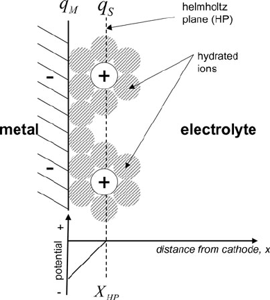
crystal lattice. That barrier is called the electric double layer. The simplest model of
the double layer structure is given by the Helmholtz model, as depicted in Fig. 3.8.
The double layer represents an organized arrangement of positive ions from the
solution to compensate for the negative charges on the surface, forming an interface
region similar to a parallel plate capacitor. The thickness of this layer is on the order
of a few nanometers [12]. The cations to be deposited have to penetrate through the
electric double layer, where they shed their hydration (or complex) shell. Then they
acquire electrons in the reduction process and become adsorbed adatoms.
The final step in the formation of a crystalline metal deposit is the incorporation
of the adatoms into the lattice. The adatoms are preferentially incorporated at active
lattice sites such as grain boundaries, imperfections, or pre-existing built-up adatom
3 Additive Processes for Metals 151
(a)
(b)
Fig. 3.7 Concentration of metal ions as a function of distance from the cathode (a) for direct
current plating and (b) for pulse current plating
clusters on the surface. If the adsorption of an adatom ensued away from an energet-
ically stable position, surface diffusion may transport the adatom to another active
lattice site on the surface. The process of either building new grains (nucleation) or
contributing to the growth of existing grains defines the formation of metal deposits
in electroplating. Additional inhibitors in a plating bath can influence this nucleation
152 D.P. Arnold et al.
Fig. 3.8 Helmholtz model of
the electric double layer. X
HP
outer Helmholtz plane; q
−
M
negative-charged metal
surface; q
S
positive-charged
solution side of the interface
and therefore the growth processes that affect the properties of the deposit such as
hardness, internal stress, and so on.
3.3.1.3 Overpotential
In the equilibrium condition (absence of external current), the potential of an elec-
trode is denoted as E
h
. As a result of a current flowing through the electrolyte the
potential of the given electrode is changed to E. The difference between these two
potentials is defined as overpotential
η = E − E
h
(3.3)
The overpotential arises from the different electrochemical mechanisms associ-
ated with the reactions and movement of the ions or adatoms. The total overpotential
is the sum of the individual overpotentials associated with each of these mecha-
nisms. As a result, any one can be rate-determining for the electrodeposition. The
diffusion overpotential η
diff
arises due to mass transport through the diffusion layer.
If this step is the slowest, the reaction is called diffusion-controlled. The activation
overpotential η
act
is associated with transfer of ions and electrons across the electric
double layer and the transfer of the electrons. Therefore η
act
is directly related to the
electrode material. If the ion and electron transfer at the metal–solution interface is
the most inhibiting step, the process is considered activation-controlled. The process
by which the uncharged adatoms either form new grains or contribute to the growth
of existing grains is associated with the crystallization overpotential η
crys
.Ohmic

3 Additive Processes for Metals 153
overpotential η
ohm
stems from the resistivity of the electrolyte. Although the contri-
bution of each overpotential deserves consideration, the activation overpotential or
the diffusion overpotential usually dominates.
3.3.1.4 Bath Composition
Every electrolyte contains metal salts. In addition, different inorganic or organic
substances are added to improve either the performance of the electrolyte solution
(e.g., conductivity) or the deposit quality (e.g., hardness, internal stress). Still other
additives can be used for specific purposes. For example, saccharin is used to reduce
the internal stress of nickel deposits [13], bromide is used for nickel anode activation
[14], and As(III)-salt is used for brightening, grain-refining, and hardening of gold
deposits [15]. Table 3.2 lists some typical additives and their function.
Table 3.2 Example chemical constituents of electrolyte solutions and their function
Type of substance Function Example
Metal salt Provide metal ions Ni(II)-sulfamate,
Cu(II)-sulfate
Wetting agent
(surfactant)
Reduce surface tension of electrolyte Laurylsulfate, Fluorinated
alkylsulfonates
Weak acid Buffer the pH Boric acid
Complexing agent Stabilize electrolyte
Influence selectivity of deposition
process in alloy plating
1,2-Ethylendiamine
Citrate
Salt Increase conductivity of electrolyte Sodium chloride
Brightener Enhance or cause a bright surface of the
deposit
Thiourea
Leveler Reduce the surface roughness of the
deposit
Coumarin
3.3.1.5 Current Waveform
In electroplating, besides the simple direct current, a variety of current mod-
ulations can be applied, such as triangular-, sawtooth-, or rectangular-shaped
waveforms. Rectangular waveforms can be further divided into two characteristic
variants: unipolar and bipolar current waveforms, both of which are commonly used.
Table 3.3 illustrates the current-time-function of direct current, pulse forward cur-
rent, and pulse reverse current. These current modulation schemes affect the plating
mechanism and thus the chemical and microstructural properties of the deposited
layer [16].
As can be seen in Table 3.3, the simplest case is the direct current mode. In con-
trast, the current waveform for pulsed electrodeposition (forward current) consists
of cathodic pulses (t
c
), separated by a current pause (t
p
). Pulse reverse electrode-
position consists of a cathodic pulse (t
c
), followed by an anodic pulse (t
a
), where
the current is reversed for a short time. In addition, the cycle can be extended
