Gersten J.I., Smith F.W. The Physics and Chemistry of Materials
Подождите немного. Документ загружается.

SYNTHESIS AND PROCESSING OF MATERIALS 363
Another method used to reduce the hydrogen content is increasing T
s
, which leads
to increased mobility of the H atoms within the films, and their recombination into
H
2
molecules, which can then diffuse to and desorb from the film surface. Higher
deposition rates are also possible at higher T
s
. The use of higher T
s
allows greater
atomic diffusion to occur in the films, which aids in the annealing (i.e., healing) of
defects. Film stress and morphology are also strongly dependent on T
s
as well as on
ion bombardment.
Changes in the PECVD growth conditions, such as increasing the partial pressure of
H
2
in SiH
4
/H
2
mixtures, increasing the power density or the frequency of the plasma, or
increasing the substrate temperature T
s
, can lead to the deposition of microcrystalline
µc films such as µc-Si:H. These µc-Si:H films have microstructures consisting of
variable volume fractions of Si nanocrystals in an a-Si network. Preferential etching
of the more weakly bonded amorphous component by H atoms is likely to play an
important role in the deposition of
µc-Si:H films.
In addition to deposition, reactive plasmas can also be used in a wide variety
of etching processes, such as those used in the fabrication of Si devices. Some of
these etching applications are discussed in Section W21.8. The plasma hardening of
metal surfaces by the implantation of N or C ions, discussed in Section W21.13, and
plasma doping by implantation of B ions into Si are also important materials processing
procedures.
Another plasma-related mode of film deposition makes use of the physical sputtering
of atoms from a target in, for example, an Ar plasma. The target material, as well as the
deposited layer, can be a metal, semiconductor, or an insulator. The sputtered atoms
are incident on the substrate, where they lead to the desired layer deposition. Physical
sputtering is typically used for the deposition of metal films.
In another mode of operation, known as reactive sputter deposition, additional
precursor gases are introduced into the plasma, where they are excited. These excited
species contribute to the layer deposition since they can react with the target atoms both
at the surface of the growing film and on the surface of the target. This method can
readily be used to control the composition of the deposited layer. Reactive sputtering
is typically used for the deposition of compound films such as oxides (including the
high-T
c
superconducting copper-based oxides), nitrides, carbides, and silicides. Typical
precursor gases include O
2
and H
2
O for oxygen, NH
3
and N
2
for nitrogen, CH
4
and
C
2
H
2
for carbon, SiH
4
for silicon, and H
2
when hydrogen is to be incorporated, as
in a-Si:H.
W21.8 Fabrication of Si Devices
A brief overview of the important steps involved in the fabrication of Si-based elec-
tronic devices from Si wafers of sufficiently high resistivity is presented next. To
illustrate the complexity of the process, consider the fabrication of a 256-Mbit dynamic
random-access memory (DRAM). A wafer yields 16 chips, each 25 mm square and
consisting of ³ 3 ð 10
8
devices with features as small as 0.25 µm. Due to the large
number ³ 300 of synthesis and processing steps involved in IC fabrication, it is not
possible here to describe these procedures in detail. Wolf and Tauber (1990) and Maly
(1987) provide useful descriptions of the steps involved in IC fabrication. Some of the
important steps have already been described (e.g., the CVD of epitaxial Si films and
the PECVD of silicon nitride dielectric films). The thermal oxidation of Si to form
364 SYNTHESIS AND PROCESSING OF MATERIALS
passivating and protecting a-SiO
2
layers is discussed in Chapter 21. Other steps, such
as diffusion (Chapter 6) and ion implantation (Section W21.3), are also discussed else-
where. Therefore, only some additional details and current issues relevant to Si device
fabrication are presented here.
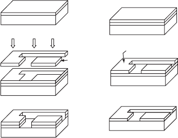
Thermal Oxidation of Si. The thermal oxidation of Si to form layers of a-SiO
2
is
repeated often during the fabrication of Si-based devices. In addition to protecting and
passivating the surface of Si, oxide layers are also used as the surface for photoresist
deposition, as masks for dopant diffusion, and as buried dielectric layers to isolate
components of the device structure. Repeated oxidations of a given Si substrate can be
carried out as often as necessary for the patterning of different circuit configurations via
the photolithographic process, described later. For example, windows can be opened
into an a-SiO
2
layer which can be used as diffusion masks, first for p-type doping into
a n-type layer and then for n-type doping into the resulting p-type region in order to
fabricate an npn transistor. This type of process is illustrated in Fig. W21.15.
The oxide dielectric layers include the thin gate oxides separating a metallic gate
from, for example, the p-type region of a MOSFET, thicker field oxides which isolate
transistors from metallic interconnecting wires, and dielectric caps which protect the
device from the surrounding environment. Gate oxide thicknesses are typically ³ 15
to 100 nm and are expected to decrease to the range 3.5 to 4.5 nm, and those of field
oxides are ³ 0.3to1
µm. These oxide layers are fabricated via the usual thermal
oxidation process or via a plasma deposition process, discussed later. Thin gate oxides
often include a region incorporating nitrogen (i.e., an oxynitride layer), which serves
to suppress diffusion of boron from the polysilicon gate into the MOSFET channel.
The Si/a-SiO
2
interfaces can be prepared to be atomically or chemically abrupt,
at least to within 0.5 nm, the dimensions of an Si–O
4
tetrahedron, and are flat on
the scale of hundreds of nanometers. Nevertheless, the actual width of the interface
(i.e., the region in which the properties of the Si and a-SiO
2
differ from their bulk
n
n
n
+
n
p
p
p
n
+
n
n
+
n
+
n
+
n
+
SiO
2
SiO
2
SiO
2
Al
(a)
(c)
(b)
(d)
Figure W21.15. Fabrication of an npn transistor involving repeated oxidation, lithographic, and
diffusion processing steps. In the case shown windows are created in an a-SiO
2
layer which can
then be used as diffusion masks, first for p-type doping into a n-type layer and then for n-type
doping into the resulting p-type region. (From B. Sapoval et al., Physics of Semiconductors,
Springer-Verlag, New York, 1993.)
SYNTHESIS AND PROCESSING OF MATERIALS 365
values) has been found to be ³ 3 nm from sensitive core-level spectroscopies which
can determine the strain in Si–O–Si bonding units. The properties of these interfaces
are critically important for the operation of devices, and their physical and chemical
structures and properties are discussed in Section 20.11.
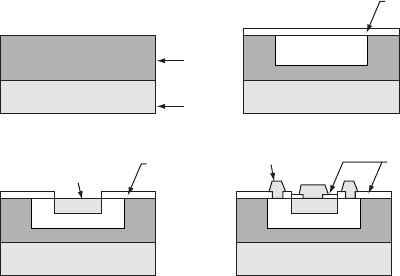
Lithography. Optical lithography (i.e., photolithography) involves the patterning of
two-dimensional circuits or designs onto Si wafers by means of the passage of light
through a mask that corresponds to the outline of the desired circuit. This is illustrated
in Fig. W21.16 and consists of the following sequence of steps:
1. A uniform a-SiO
2
layer is deposited onto the Si.
2. The a-SiO
2
layer is then covered by a layer of photosensitive polymeric material
known as a photoresist. The photoresist is applied as a uniform liquid layer, using
a spin-on procedure that is discussed in Section W21.24, and is then solidified
via the application of heat.
3. The photoresist undergoes polymerization or cross-linking during exposure to
light through a mask; this is the photoresist development step.
4. In the case illustrated involving the use of a negative photoresist, the unillu-
minated and hence unpolymerized areas of photoresist are removed via etching
with an appropriate chemical solvent.
5. The exposed a-SiO
2
pattern is removed via etching using an acid that does not
attack the polymerized photoresist.
6. The polymerized photoresist is finally removed via another suitable chemical
solvent.
The patterned a-SiO
2
layer that remains on the surface can act as an insulating layer
in the structure or can be used as a diffusion barrier in a subsequent processing step.
The predominant method of photoresist removal is currently the use of oxygen plasmas
which are described later in the discussion of etching processes.
(a)
(c)
(e)
(b)
(d)
(f)
SiO
2
Si
UV radiation
Hardened photoresist
Photo mask
Lacquer
Figure W21.16. Optical lithography process involving the patterning of two-dimensional
circuits or designs onto wafers through the use of light passing through a mask. (From B. Sapoval
et al., Physics of Semiconductors, Springer-Verlag, New York, 1993.)

366 SYNTHESIS AND PROCESSING OF MATERIALS
The interaction of light with photoresist materials such as the high-molecular-weight
polymer polymethylmethacrylate (PMMA, also known as Plexiglas or Lucite)
is discussed in Section 14.10. The light-induced breaking of bonds (i.e.,
photodissociation) in the long polymeric chains in the illuminated portions of the
PMMA photoresist layer renders these regions susceptible to removal via etching.
There are two types of photoresists in use: negative photoresists, which undergo light-
induced cross-linking and so become insoluble and harder to remove after illumination,
and positive photoresists like PMMA, which undergo light-induced chain breaking
and so become more soluble and easier to remove after illumination. While negative
photoresists are usually more photosensitive than positive photoresists and require
less illumination, they have lower resolution and hence their use is not desirable in
high-density ICs. PMMA is the photoresist with the highest-known resolution.
As the dimensions of features in ICs continue to decrease below 0.25
µm, optical
lithography using UV light (e.g., the ArF laser line at D 193 nm) may no longer be
possible since the minimum size of a feature is controlled by diffraction effects that
limit the definition of the image to about one-half of the wavelength of the light used.
The resolution limit D is given by
D D
2sin8
,W21.20
where 8 is the angle subtended by the mask opening at a point on the surface and sin 8
is the numerical aperture (NA). For an opening of width w that is a height H above
the substrate, tan 8 D w/2H. The corresponding depth of focus, h,isgivenby
h D
sin
2
8
.W21.21
Another important length scale governing the exposure depth is 1/˛, the inverse of the
absorption coefficient of the light in the photoresist.
Nanolithographic technologies (i.e., technologies with the higher resolution needed
for producing geometrical circuit features with sizes below ³ 0.1
µm) are based on
shorter-wavelength beams of electrons or x-rays, or on the use of scanning probe micro-
scopies such as scanning tunneling microscopy (STM) and atomic force microscopy
(AFM). These advanced technologies are being explored as alternatives to optical
lithography. Electron beams have the advantages of being able to be steered and focused
rapidly using electric and magnetic fields. There are as yet no suitable photoresist
materials for features smaller than 0.1
µm.
In the LIGA process (lithographie galvanoformung abformung), synchrotron radia-
tion is employed to expose the photoresist polymer PMMA. Exceptionally sharp walls
are produced, resembling steep cliffs. Metallization of the structure can even result in
excellent molds from which replicas may be cast.
Diffusion. The thermal diffusion of dopants into a device in order to create junctions
between n-andp-type regions, or just to change the electrical resistivity of a region,
occurs repeatedly during device fabrication. Since solid-state diffusion is discussed in
Chapter 6, only some details relevant to Si device fabrication are mentioned here.
Due to the need to limit the region of doping in the substrate, all diffusion
processes are preceded by oxidation and mask-patterning lithographic steps. Layers
SYNTHESIS AND PROCESSING OF MATERIALS 367
of a-SiO
2
serve as good mask materials for diffusion processes due to the low
diffusion coefficients of typical dopants in the oxide. At typical diffusion temperatures
of T D 900 to 1100
°
C, dopants present in a source at the Si surface will diffuse through
the opening in the mask into the Si both vertically (i.e., normal to the surface), and
laterally.
Two methods of dopant diffusion are typically used, constant-source diffusion or
two-step diffusion. In the first method, used when shallow junctions are desired, a thick
layer consisting of a mixture of B
2
O
3
or P
2
O
5
and SiO
2
is deposited onto the surface.
This layer acts as a constant source of dopant atoms, so the dopant concentration at
the surface remains essentially constant as diffusion occurs deeper and deeper into
the substrate (see Fig. W6.2). The second method, used when deeper junctions are
desired, starts with a predeposition step which is essentially the same as the constant-
source method. After removal of the dopant source from the surface, a second, high-
temperature step is used to drive the dopant atoms farther into the substrate (see
Fig. W6.1).
Complicating the diffusion of acceptors such as B in Si are the effects known as
oxidation-enhanced diffusion (OED) and transient-enhanced diffusion (TED). OED
and TED both result from the injection of excess Si interstitials into the Si substrate
and away from the Si/a-SiO
2
interface in the case of OED and out of a damaged ion-
implanted layer in the case of TED. Dopants such as B must pair with defects such as
vacancies or interstitials to move through the lattice, and as a result, their diffusion is
affected by the motion of excess interstitials.
Ion Implantation. Ion implantation is used as an alternative to the introduction of
dopants by diffusion in IC fabrication when the high temperatures associated with
diffusion cannot be tolerated. In addition, the lateral spreading of dopants associated
with the diffusion process is minimized when ion implantation is used, a significant
advantage in high-density devices. As with diffusion, implantation occurs through a
mask and extends into the Si for a characteristic distance known as the range.Themask
is an opening in an a-SiO
2
overlayer or any other overlayer (metal, photoresist, etc.).
Some of the important aspects of ion implantation are discussed in Section W21.3. The
dose and energy of the implanted ions determine the doping level and the position of
the resulting junction within the implanted Si. When desirable, implantation through
a thin overlayer is possible as long as the incident ions are sufficiently energetic.
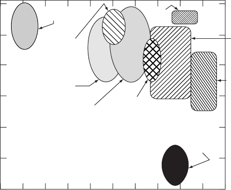
A schematic phase-space map of the typical ion energies (in electron volts) and ion
beam currents (in particle-amperes) used in semiconductor processing is illustrated in
Fig. W21.17.
The lattice disorder created in the Si by the incident energetic ions can lead to
dopant deactivation when the dopant atoms do not enter the lattice substitutionally or
when traps are generated. A subsequent annealing step must then be carried out to
repair the damage and for dopant activation.
When plasmas are used to excite the species to be implanted, the process is known
as plasma-immersion ion implantation (PIII). In this method the substrate is immersed
directly in the plasma, and rather than using accelerated beams of energetic dopant
ions, high fluxes of relatively low-energy dopant ions are instead extracted from the
plasma by applying pulsed high negative voltages, ³ 2 to 4 kV, to the substrate. When
PIII is used to form shallow p
C
-n junctions, the n-type Si substrate is first converted
to amorphous Si by using SiF
4
in the plasma, followed by the introduction of BF
3
to
368 SYNTHESIS AND PROCESSING OF MATERIALS
Beam current [particle-amperes]
Molecular beam
epitaxy
Etching
ion milling
Ion beam deposition
ion cluster beam
Plasma
immersion
implant
Low-energy
implant
Focused ion
beams
SIMOX
"Routine"
implantation
High-energy
implant
10
−10
10
−2
110
2
10
4
10
6
10
−8
10
−6
10
−4
10
−2
1
Energy [eV]
Figure W21.17. Schematic phase-space map of the typical ion energies (in electron volts) and
ion beam currents (in particle-amperes) used in semiconductor processing. (From E. Chason
et al., J. Appl. Phys., 81, 6513 (1997). Copyright 1997 by the American Institute of Physics.)
the plasma to implant B ions into the a-Si. An extremely shallow junction depth of
80 nm can be achieved following thermal activation of the dopant atoms using rapid
thermal annealing of the implanted region at T D 1060
°
C for 1 s. The PIII process for
dopant implantation is similar to the plasma carburizing and nitriding processes used
to modify the surface properties of metals, as discussed in Section W21.13.
In the process known as separation by implantation of oxygen (i.e., SIMOX) a buried
dielectric layer is created below the surface of a Si substrate via the implantation of
oxygen ions. This process is a major candidate for the creation of Si-on-insulator (SOI)
structures in which devices are isolated by being surrounded completely by an insulator
rather than by using a reverse-biased p-n junction. The O
C
implantation consists of
a high dose, ³ 2 ð 10
18
cm
2
, of ions, which leads to the formation of a continuous
buried a-SiO
2
layer following an annealing step for 3 to 5 h at T D 1100 to 1175
°
C.
The characteristic distance of the buried layer from the Si surface is 0.3 to 0.5
µm
when O
C
ion energies of 150 to 180 keV are used.
Chemical and Physical Vapor Deposition. A variety of chemical and physical
vapor deposition procedures are used to deposit the conducting, semiconducting, and
insulating layers that are needed in device fabrication. Reactions between the incident
vapor species and the substrate are not necessarily required to grow the desired films
in these CVD and PVD procedures. As an example, a-SiO
2
layers must be deposited
via PECVD when this dielectric layer is to be grown on a metallic layer instead of
on Si. The CVD of epitaxial Si layers and the PECVD of the silicon oxide, nitride,
and oxynitride layers used as dielectrics for interlevel isolation, for passivation, and
as gate insulators have already been discussed. Si epilayers can be deposited on Si
substrates with differing doping levels (e.g., an n-type Si epilayer deposited onto an
SYNTHESIS AND PROCESSING OF MATERIALS 369
n
C
Si substrate). PVD in the form of electron-beam evaporation or sputtering is used
for the deposition of Al layers.
A challenging problem is the deposition of conformal layers (i.e., layers of uniform
thickness) on nonplanar substrates having steps, trenches, and holes. Examples of relia-
bility problems in devices due to deposited layers with nonuniform thicknesses include
inadequate electrical isolation in dielectric layers and nonuniform current densities in
conducting layers, leading to enhanced electromigration in the conductors and hence
open circuits. In the case of a-SiO
2
deposition, when mixtures such as SiH
4
/Ar/N
2
Oor
SiH
4
/Ar/O
2
are used, the sticking coefficients for SiH
n
species are high, with the result
that the a-SiO
2
layers tend not to be conformal. A method for obtaining conformal
a-SiO
2
layers is plasma deposition using the liquid tetraethoxysilane (TEOS) as the
source of the precursor in mixtures with O
2
or O
3
(ozone) and Ar. Oxide depositions
using dilute TEOS/O
2
mixtures at T D 200 to 300
°
C result in lower deposition rates,
< 50 nm/min, compared to SiH
4
-based depositions, but the resulting layers have good
conformality, due to the low sticking coefficients and higher surface mobility of the
TEOS-based precursors.
Metallization. Aluminum and Al alloys have been the metals of choice for providing
the electrical connections between circuit elements in ICs due to their desirable physical
and chemical properties (e.g., excellent electrical conductivity, the ability to form both
ohmic and Schottky barrier contacts to Si, good bonding and adherence to both Si
and SiO
2
and also to diffusion barriers such as TiN and Ti, the ability to be patterned
in Cl-based plasmas, and the ability to form a stable oxide, Al
2
O
3
, when exposed to
air). Aluminum alloyed with 0.5 wt % Cu exhibits higher hardness and good electrical
conductivity, along with improved resistance to electromigration, a process described in
Section 12.9. The resistance to electromigration resulting from alloying Al with Cu is
attributed to the precipitation of Cu at grain boundaries. This inhibits the harmful grain-
boundary diffusion of Al, which leads to vacancy accumulation and void formation in
the Al connecting lines. Even though Cu itself has low electrical resistivity and good
resistance to electromigration, it has not been widely used so far as an interconnect
metal because a successful dry-etching process has not been developed for patterning
the Cu lines. In addition, diffusion barriers must be used between Cu lines and Si
because Cu impurity atoms act as deep traps in Si.
Problems with Al layers deposited by PVD methods such as electron-beam evapo-
ration and dc magnetron sputtering are associated with incomplete filling of vias and
with poor step coverage for feature sizes below 0.5
µm. Other possible deposition
procedures that may lead to improved via filling and step coverage include high-
temperature Al-alloy sputtering processes, the use of Al reflow processes, and CVD at
T D 100 to 200
°
C using Al-containing metal–organic molecules at deposition rates of
100 to 200 nm/min. Aluminum reflow processes involve the use of elevated deposi-
tion temperatures or postdeposition annealing to allow the deposited Al alloy to flow
into and fill via/contact holes. The Al-alloy reflow temperatures lie below the alloy
melting points by ³ 150
°
C, with both temperatures decreasing with increased alloying
of elements such as Cu or Ge.
The refractory metal W can be selectively deposited via CVD and allows much
better step coverage and via and hole filling than Al. In addition, it exhibits excel-
lent resistance to electromigration. Bilayers of Ti and TiN serve as diffusion barriers
between W and Si and also as intermediate layers for the CVD of W. The initial Ti
370 SYNTHESIS AND PROCESSING OF MATERIALS
layer is reacted with the underlying Si at T ³ 700
°
C to form a titanium silicide Ti
x
Si
y
phase with both good electrical conductivity and contact to the underlying Si. A TiN
x
diffusion barrier layer is then deposited to prevent undesired reactions between the
Ti
x
Si
y
layer and the fluorine involved in the CVD of W via the hydrogen reduction of
the WF
6
precursor [i.e., WF
6
g C 3H
2
g ! Ws C 6HFg]. When selective depo-
sition of W and lower deposition temperatures are required, the silane reduction of
WF
6
can be used [e.g., 2WF
6
g C 3SiH
4
g ! 2Ws C 3SiF
4
g C 6H
2
g].
Local interconnects formed from low-resistivity doped polycrystalline Si layers are
useful because these layers can make good electrical contact to Si substrates and can
also serve as diffusion barriers between Si and Al lines. Electrical contacts between
pure Al and n
C
and p
C
Si are not stable at processing temperatures in the range
T D 350 to 500
°
C, due to the solubility of Si in Al and also to the rapid diffusion of
Si into the polycrystalline Al contacts. The reciprocal diffusion of Al into the Si layer
can lead to the spiking (i.e., shorting) of shallow junctions. The use of polysilicon
is restricted to buried contacts and to limited regions due to its relatively high sheet
resistance of 20 to 30 5/square.
Etching Processes. Device fabrication involves a variety of processing steps
employing the etching or controlled removal of material from the surface of the wafer.
The etching or stripping process can employ either wet, liquid-phase or dry, gas-
phase etchants. Chemical etching, in which the etchant reacts with the material to be
removed, can occur in either the liquid or gas phases, is typically highly selective, and
is isotropic (i.e., the etching occurs at the same rate in all directions). Physical etching
is a gas-phase process in which material is removed by sputtering (i.e., via energy and
momentum transfer from incident ions), is less selective than chemical etching, and
is typically anisotropic (i.e., etching occurs preferentially in one direction). Selectivity
refers to the ability of the etching process to remove some materials but not others.
An example is positive-photoresist lithography, where liquid solvents etch away the
illuminated portion of the photoresist while the unilluminated portion is unaffected, or
as when an HF acid etch is used to remove a-SiO
2
but neither Si nor photoresist.
A plasma etching process with both chemical and physical components is reactive-
ion etching (RIE), in which ions created in a plasma react with and also transfer kinetic
energy to the material to be etched. An advantage of RIE is that it can be both selective
and anisotropic. Plasma etching is used for the removal of Si, of a-SiO
2
and silicon
nitride, of metals, and of photoresist. Appropriate etching species are chosen for each
case: for example, F atoms and Ar
C
ions for etching Si or polysilicon (forming SiF
4
)
and O atoms for etching or stripping photoresist (forming CO, CO
2
,andH
2
O). The
Ar
C
ions provide additional kinetic energy, which can greatly increase the yield of
the etching process by enhancing chemical etching reaction rates on the surface. For
example, a 1-keV Ar
C
ion can result in the removal of up to 25 Si atoms when a flux
of F atoms is also incident on the surface. The use of Ar
C
ions can also increase the
anisotropy of the etching but may decrease the etching selectivity.
Etch inhibitors are also used in RIE to prevent etching from occurring outside
the area exposed to the ion beam. An example is the anisotropic etching of trenches
and holes in Al using CCl
4
/Cl
2
mixtures, where the CCl
4
molecules are the inhibitor
precursors. A protective, etch-inhibiting amorphous chlorocarbon film is present on the
areas of the Al surface not exposed directly to the ion beam, including on the sidewalls

SYNTHESIS AND PROCESSING OF MATERIALS 371
of the features being etched. The presence of C in the etching mixture thus leads to
an enhancement of the anisotropic etching of the desired trenches and holes.
Reactive-ion etching rates are very difficult to predict. This is due to difficulties
associated with modeling the plasma processes giving rise to the incident fluxes of
reactive atomic and molecular radicals and ions on the surface. There are also diffi-
culties with modeling the many surface processes, including adsorption, diffusion,
reaction, and desorption, involved in the generation of etching products. In addition,
in the F etching of Si, a fluorinated SiF
x
surface layer two to five monolayers thick is
present and the diffusion of the etching species, F
ions, through this layer plays an
important role in the process. A rough estimate for the characteristic thickness of this
layer is d ³ D/R
e
Si,whereD is the diffusion coefficient for F
ions in the surface
layer and R
e
Si is the etching rate in m/s.
The etching of Si by halogen atoms such as F and Cl is found to depend on the
doping level and type of the Si substrate, with etching rates of n-type Si exceeding
those of p-type Si by a factor of about 2 for F and by many orders of magnitude for Cl.
These observations indicate that the position of the Fermi level and the concentrations
of charge carriers near the Si surface can play important roles in the etching process.
The current model is that electrons in n-type Si tunnel from the bulk through the SiF
x
layer, leading to the formation of F
or Cl
ions that attack Si–Si bonds in either
the surface layer or the bulk. Molecules such as CF
4
are typically used as etching
precursors because the etching of Si by F
2
leads to roughening the surface through
pitting. The overall etching reaction in this case can be written as
4CF
4
C Si ! SiF
4
C 2C
2
F
6
.W21.22
When wet chemical etching is used to remove an unprotected a-SiO
2
layer, the
isotropic nature of the etching can cause unwanted undercutting of the oxide beneath the
protective photoresist mask. As a result, the pattern obtained is not the one desired. Dry
etching carried out at reduced pressures in the gas phase can combine the advantages
of chemical etching in being selective and physical etching in being anisotropic, so
that no undercutting of the oxide occurs.
The smallest feature size (e.g., the minimum trench width) that can be obtained via
etching is
w ³
2d
a
h
,W21.23
where d is the depth of the trench and a
h
D R
ev
/R
eh
is the ratio of the vertical and
horizontal etch rates of the material in which the trench is being etched. As an example,
0.2-
µm-wide and 4-µm-deep trenches with the aspect ratio d/w D a
h
/2 D 20 can be
etched into single-crystal Si using F-based chemistry.
Remaining problems associated with the use of plasmas in device fabrication are
related to ion-induced damage and plasma-induced contamination.
Annealing. Annealing at elevated temperatures is often required in IC fabrication for
a variety of purposes:
1. To remove, or at least minimize, processing-induced defects (e.g., those created
in the Si lattice during ion implantation).
372 SYNTHESIS AND PROCESSING OF MATERIALS
2. To activate implanted dopants in Si or polysilicon following ion-implantation
procedures.
3. To drive dopant atoms farther into the Si following their implantation in a shallow
layer.
4. To promote the reactions between deposited metals such as Ti and the underlying
Si in order to form desired silicides.
5. To deactivate deep trap-generating impurities such Cu and Fe via gettering, a
process in which these impurities diffuse to and are immobilized in the strain
fields of extended defects such as oxide precipitates or dislocations. In this way
the traps are removed from the active area of the device.
The time and temperature of an anneal must be chosen so that unwanted dopant
redistribution does not occur. Any exposure of the device to high temperatures must
therefore be as brief as possible. A method for limiting the annealing time is the
process of rapid thermal annealing (RTA), also known as rapid thermal processing
(RTP). A typical RTA dopant drive-in procedure involves a rapid temperature increase
to T D 1050 to 1150
°
C, a 10-s anneal, and a rapid decrease to temperatures at which
diffusion is negligible.
W21.9 Processing of Microelectromechanical Systems
The fabrication of Si-based microstructures for use in microelectromechanical systems
(MEMS) having typical dimensions ³ 1to100
µm is an exciting new area of materials
research.
†
In addition to its well-known and extremely versatile electronic properties,
crystalline Si also possesses very useful mechanical and thermal properties, such as
high durability, elasticity, and thermal conductivity, which can be exploited in very
small electromechanical structures. With the development of MEMS, Si semiconductor
device-fabrication technology can now also be exploited in sensors and actuators for
measurement and control in the fields of thermodynamics, optics, magnetism, acous-
tics, and hydrodynamics. Besides Si, other materials used in MEMS include a-SiO
2
,
crystalline quartz, and other ceramics, such as SiC. Since MEMS technology is in a
state of rapid development, only a brief survey is given here.
The fabrication of MEMS is involved primarily with the processing of Si wafers
into the desired final forms using a variety of etching and micromachining procedures.
These processing procedures currently include the following:
1. Anisotropic wet chemical etching, usually in KOH solutions
2. Dry etching (i.e., reactive-ion etching) with the etchant activated via plasma
excitation
3. Surface micromachining involving the removal of a sacrificial layer of a-SiO
2
or
porous Si via etching in HF
4. Porous Si technology, also involving surface micromachining but using much
thicker sacrificial layers of porous Si, up to hundreds of micrometers thick
†
A recent review article is W. Lang, Mater. Sci. Eng., R17, 1 (1996).