Gersten J.I., Smith F.W. The Physics and Chemistry of Materials
Подождите немного. Документ загружается.

SYNTHESIS AND PROCESSING OF MATERIALS 353
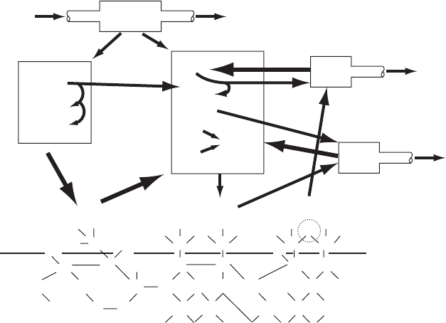
Exhaust
Standard
taper
joint
RF coil
Quartz
sled
Water
Flowmeters
Molecular sieve
traps
H
2
Filter
Palladium
diffuser
3%
SiH
4
in He
100
PPM
AsH
3
in He
100
PPM
B
2
H
6
in He
Valves
Exhaust
Exhaust
HCl
He
Wafers
Susceptor
Figure W21.10. Typical cold-wall Si CVD system. (From D Richman et al., RCA Review, 31,
613 (1970).)
heated substrate surface. The hydrodynamics of the flowing gases in the CVD system
can have a significant influence on the growth process.
In the case of Si CVD, there are many possible choices for the molecular precursors,
including SiH
4
and SiHCl
3
. The important growth species present on the surface are
then the highly reactive radicals silylene, SiH
2
,andSiCl
2
. These radicals are the
products of the thermal decomposition of the feedstock gases and will undergo further
reactions on the surface of the growing film. Carrier gases such as H
2
and He are often
used to aid in the transport of vapor species to the substrate. The concentrations of
atoms, radicals, and molecules adsorbed on the growing surface are controlled by their
incident fluxes (i.e., by their partial pressures in the vapor phase) and by the substrate
temperature T
s
which controls their desorption rates.
Typical net chemical reactions resulting in the growth of the Si epilayer include the
following:
SiH
4
g ! Sis C 2H
2
g,
2SiHCl
3
! 2Sis C 3Cl
2
g C H
2
g.
W21.17
These reactions actually represent a series of elementary steps taking place in the vapor
phase and on the substrate surface. Growth rates are ³ 1
µm/ min at T
s
³ 1100
°
Cand
decrease rapidly as T
s
is lowered (see Fig. 21.3). Homogeneous vapor-phase reactions
leading to the formation of disilane Si
2
H
6
are
SiH
4
g ! SiH
2
g C H
2
g,
SiH
4
g C SiH
2
g ! Si
2
H
6
g.
W21.18

354 SYNTHESIS AND PROCESSING OF MATERIALS
These reactions can ultimately lead to the formation of undesirable polymeric silicon
hydride powder, SiH
2
n
.
The partial pressures of the vapor species involved in growth must exceed their
equilibrium vapor pressures with respect to the Si surface at T
s
in order for the net
deposition of a film to occur. The growth species must therefore be supersaturated
in the vapor phase, with the supersaturation ratio SSRforthecaseofSi(g)atoms
defined by
SSRSig, T
s
D
PSig
P
eq
Sig, T
s
,W21.19
where PSig is the actual vapor pressure of Si(g) just above the substrate surface
and P
eq
Sig, T
s
is the equilibrium vapor pressure of Si(g) with respect to pure Si(s).
A wide variety of investigations have allowed the following conclusions to be
reached concerning the growth of Si epilayers via CVD:
1. The rate-controlling step for the growth of Si is either the removal from the
surface of hydrogen in Si–H bonds via the desorption of H
2
, or the dissociation
of SiH
2
or SiCl
2
on the surface.
2. The rate-controlling step for obtaining high crystallinity in the Si epilayer is the
diffusion of Si on the growing surface.
3. Lattice defects are generated when the Si adsorption rate exceeds the rate at
which Si can diffuse on the surface and be incorporated into the growing film.
Si atoms then enter nonideal, higher-energy bonding configurations.
4. Si atoms compete with other species on the surface, such as dopant atoms or
molecules and hydrogen, oxygen, or carbon atoms, for the available bonding
sites to Si substrate atoms, thereby limiting the Si atom diffusion rate.
The termination of the growing Si surface by hydrogen in Si–H bonds can play
a critical role in the CVD of Si by inhibiting epitaxial growth through the blocking
of surface sites for the adsorption of reactive species such as SiH
2
and SiH
3
.Thisis
particularly important at T
s
less than about 400 to 500
°
C.
Recently, the CVD of Si and of Si–Ge alloys has been combined with UHV tech-
niques to achieve a very high level of system and substrate cleanliness (e.g., the
elimination of oxygen and carbon surface impurities). The use of this growth method,
known as UHV/CVD, allows the deposition of epitaxial Si and Si–Ge layers at much
lower pressures, P ³ 10
3
torr, and lower T
s
, ³ 500 to 550
°
C, than are ordinarily
used. Operation at lower pressures has several advantages: the undesirable homoge-
neous pyrolysis of precursors in the vapor phase is minimized, the very low partial
pressures of O
2
and H
2
O necessary for the maintenance of an active, SiO
2
-free Si
surface are more readily achieved,
†
and molecular flow conditions are obtained, with
the result that recirculating flows, eddy currents, and turbulence are avoided. Due to
the clean and hydrogen-stabilized surfaces of the Si wafers when they are placed into
†
For experimental results and discussions of the interactions of O
2
and H
2
O with Si at high temperatures,
seeF.W.SmithandG.Ghidini,J. Electrochem. Soc., 129, 1300 (1982); G. Ghidini and F. W. Smith, J.
Electrochem. Soc., 131, 2924 (1984).
SYNTHESIS AND PROCESSING OF MATERIALS 355
the UHV/CVD system, no further in situ treatment at high temperatures is required to
prepare the Si surface for epitaxial growth.
The use of lower substrate temperatures reduces problems associated with dopant
atom redistribution via diffusion and also is a very effective method of reducing defect
concentrations in the films. Growth at lower T
s
will reduce the equilibrium concentra-
tions of defects such as vacancies and will also reduce the mobility of point defects and
hence their tendency to interact with each other to form extended defects. In addition,
thermal stresses which can also lead to the generation of defects in the film will be
reduced at lower T
s
. Better film thickness uniformity is also expected at lower T
s
since
the deposition process changes from one controlled by vapor-phase transport at higher
T
s
to one controlled by surface reactions at lower T
s
, as discussed in Section 21.3. It
is still necessary to maintain T
s
well above the range in which the film will become
noncrystalline or amorphous.
Nonequilibrium structures and alloys can also be prepared at low T
s
. These include
strained Si–Ge epilayers grown on Si with thicknesses well above the critical values
for the generation of misfit dislocations and also alloys of Si with concentrations of
dopant atoms such as B which are several orders of magnitude above equilibrium
concentrations. Sharp transitions, particularly in dopant profiles, between the substrate
and the epilayer are essential as device dimensions continue to shrink. Both the layer
growth rate and dopant diffusion rates decrease exponentially as T
s
decreases. Since
the activation energy for diffusion, E
a
diff ³ 3.5 eV, is much greater than that for
growth, E
a
growth ³ 1.5 eV, reasonable growth rates, ³ 0.1 to 10 nm/min, can still
be obtained at T
s
³ 500
°
C, where dopant diffusion has been effectively frozen out.
A schematic of the hot-wall apparatus used in the UHV/CVD method is shown in
Fig. W21.11. The carefully cleaned Si wafers have surfaces passivated by H termi-
nation (i.e., Si–H bonds), which can be thermally desorbed from the Si surface at
T
s
> 400
°
C. In the UHV/CVD of Si the vapor phase consists entirely of SiH
4
.
Films that are “defect-free” (i.e., with defect densities less than ³ 100 cm
2
)are
readily achieved via CVD. The most sensitive quantitative method of determining
Mass
spectr.
Furnace
UHV/load chamber
Gas
source
Vacuum
transfer
apparatus
Turbo
pump
Turbo
pump
Al
2
O
3
trap
Rotary pump
Rotary pump
and
roots blower
Figure W21.11. UHV/CVD system. (From B. S. Meyerson, Appl. Phys. Lett., 48, 797 (1987).
Copyright 1987 by the American Institute of Physics.)
356 SYNTHESIS AND PROCESSING OF MATERIALS
densities of structural defects such as dislocations in Si epitaxial layers is by means of
chemical etching. Since the disordered regions of the lattice containing defects are in
a state of higher energy, they are more rapidly attacked (i.e., etched) by appropriate
acids. Optical microscopy can then be used to count the etch pits and also to iden-
tify the nature of the defects from the shape of the etch pit. Transmission electron
microscopy (TEM) is the preferred method for probing the atomic perfection of the
interface between the substrate and the epilayer. Electrically active defects such as
impurity-related traps are not readily detected via etching or TEM. Their presence can
be determined by the effects that they have on devices such as diodes, transistors,
or metal–oxide–semiconductor (MOS) capacitors, which are fabricated from the Si
epilayers.
Metallic elements such as Fe and other transition metals are undesirable impurities
in Si due to the fact that they act as traps (i.e., as centers for the recombination of
electrons and holes). Although they do not enter into CZ or FZ Si from the melt due
to their very low distribution coefficients, they will diffuse rapidly into the bulk at
elevated temperatures if they can reach the surface of the Si crystal through the vapor
phase.
Other recent approaches to Si epitaxy via CVD include the use of intermediate layers
such as cubic CaF
2
, fluorite, whose lattice constant, a D 0.546 nm, matches that of Si,
a D 0.543 nm, to within 0.6% at T D 300 K. The CaF
2
layer is deposited epitaxially
onto the Si(100) surface first, followed by the deposition of the Si epilayer onto the
CaF
2
layer. The top Si epilayer is then removed for further processing by dissolving
the intermediate CaF
2
layer in an appropriate solvent. In this way the original Si(100)
substrate can be reused.
A recent approach to understanding the growth of Si epilayers at low tempera-
tures has involved the definition of a limiting epitaxial thickness h
epi
above which
the deposited films become amorphous. This is in contrast to the usual definition of a
minimum epitaxial temperature T
epi
, below which epitaxy is impossible, due to insuffi-
cient surface diffusion of atoms adsorbed on the surface. Epitaxial growth of Si can be
observed in a very clean MBE system at all temperatures between T D 50 and 300
°
C,
but only up to the thickness h
epi
, which increases exponentially with increasing T and
decreases with increasing growth rate. For Si films grown via MBE, h
epi
was found
to be 1 to 3 nm at room temperature. The transition from crystalline to amorphous
growth at h
epi
has been attributed to a surface-roughening effect, with the accumula-
tion at the growing surface of impurity atoms such as hydrogen playing a major role
in the roughening process.
W21.6 Molecular-Beam Epitaxial Growth of GaAs
The growth via molecular-beam epitaxy (MBE) of films of the group III –V semicon-
ductor GaAs, as well as of other III–V and II–VI semiconductors, has many features
in common with the CVD of epitaxial Si layers, including the steps of transport and
adsorption of the appropriate precursor vapor species onto the substrate surface, nucle-
ation and growth of the film, and removal of unwanted species from the substrate
surface. In MBE molecular beams (i.e., beams of neutral molecules or atoms) are
directed onto a heated substrate in a UHV system. Due to the low particle density of
the beam and also to the very low background pressure in the growth chamber, the parti-
cles in the beam do not interact with each other and undergo essentially no collisions
SYNTHESIS AND PROCESSING OF MATERIALS 357
Liquid nitrogen
cooled shrouds
Effusion
cell ports
HEED gun
Main shutter
Rotating substrate holder
Ionization gauge
Gate valve
Sample
exchange
load lock
View port
Effusion
cell shutters
Fluorescent
screen
To variable
speed motor
and substrate
heater supply
Figure W21.12. Typical MBE vacuum chamber. (Reprinted from A. Y. Cho, Thin Solid Films,
100, 291 (1983), copyright 1983, with permission from Elsevier Science.)
with residual gas molecules on their path from the source to the substrate. A typical
MBE growth chamber is shown schematically in Fig. W21.12. Along with the vacuum
chamber and all the associated accessories, appropriate vacuum pumps and electronics
for the control of the various components are required. The mass spectrometer is used
for residual gas analysis. It can also be used to measure the fluxes of reactant species
and can provide signals to be used for adjusting the effusion cell temperatures so that
constant fluxes, and hence constant deposition rates, can be maintained.
Advances in UHV technology
†
have permitted the deposition via MBE of films at
relatively low T
s
with unparalleled control of composition, purity, and interface sharp-
ness, involving literally atomic layer-by-layer growth. The low growth temperature has
the advantage of reducing undesirable thermally activated processes such as diffusion,
while the low growth rates ³ 10 nm/ min offer the advantage of accurate control of
film thickness. The UHV conditions employed in MBE also permit in situ monitoring
of the film structure and thickness using high-energy electron beams reflected at very
low angles from the surface of the growing film. This technique is known as reflec-
tion high-energy electron diffraction (RHEED). The chemical purity and composition
of the substrate and of the film can also be monitored in situ using Auger electron
spectroscopy (AES). Finally, the use of modulated-beam mass spectrometry (MBMS)
employing separate beams of Ga and As
2
has allowed the detailed study of surface
processes involved in the growth of GaAs via MBE.
The solids that are the source materials for the MBE of GaAs are contained in heated
effusion cells within the vacuum chamber. Elemental Ga metal is used for the Ga flux,
while solid GaAs is used for As
2
and solid elemental As for As
4
. Additional elements
†
See Weissler and Carlson (1979) for a useful description of UHV techniques.
358 SYNTHESIS AND PROCESSING OF MATERIALS
used for doping, alloying, and for multilayer or junction depositions are contained in
their own effusion cells. The nature and flux of the vapor species from each effusion
cell are controlled by the temperature of the cell, with the flux directed through a small
orifice in the wall of the cell toward the substrate. Shutters placed between each cell
and the substrate are used to block individual beams when control of the composition or
thickness of the growing film is desired. The substrates are mounted on heated holders
whose temperature T
s
can be controlled accurately by regulated internal heaters. The
substrate holders can be rotated during growth in order to obtain extremely uniform
epitaxial films.
Due to the very low background pressure in the MBE chamber during growth, P ³
10
9
torr (³ 10
7
Pa), very few unwanted residual gas molecules are incident on the
substrate and incorporated into the films. Due to the cleanliness of the growth chamber,
growth rates can be very low, 6 to 60 nm/min, which allows extremely thin layers with
abrupt interfaces to be grown on surfaces that are essentially atomically smooth. Typical
beam fluxes can be in the range 10
11
to 10
16
atoms (or molecules)/cm
2
Ðs.
The substrates used for GaAs integrated-circuit fabrication are semi-insulating bulk
GaAs crystals grown via the liquid-encapsulated Czochralski method. These undoped
substrates typically contain 10
4
to 10
5
dislocations/cm
2
. Before being placed in the
growth chamber the substrates undergo a variety of polishing, etching, and rinsing
procedures which are chosen carefully for each type of substrate. Further treatment of
the substrate within the growth chamber is also possible and typically involves heating
to about T D 580
°
C to remove oxygen, followed by Ar ion bombardment to remove
the less volatile carbon contamination. To obtain extremely clean growth surfaces,
undoped epitaxial layers of GaAs are often grown in the MBE growth chamber on
existing bulk substrates.
Stoichiometric GaAs films are typically grown in the range T
s
D 500 to 600
°
C under
an incident vapor flux that is enriched in As-containing species due to the instability of
the heated GaAs surface with respect to the preferential loss of more volatile arsenic
species. When As
2
is incident, stoichiometric GaAs films are obtained as long as the
As
2
flux exceeds 50% of the Ga flux [i.e., as long as RAs
2
/RGa>0.5]. The sticking
coefficient of Ga is equal to unity for T
s
less than about 480
°
C and then decreases
exponentially with an activation energy of E
a
³ 2.5 eV at higher temperatures. Under
proper growth conditions any excess arsenic beyond that needed for stoichiometric
growth is desorbed from the surface of the growing film. This is attributed to a high
sticking coefficient for As
2
on a Ga-terminated surface and a low sticking coefficient
for As
2
on an As-terminated surface, as observed experimentally. As a result, the
growth rate of GaAs, which is controlled by the incident monoatomic Ga flux, can
also be limited kinetically by the desorption of As-containing species that block sites
for the incorporation of Ga atoms.
The GaAs growth process from Ga and As
2
has been shown by sensitive MBMS
and RHEED studies to be limited by the first-order dissociative chemisorption of As
2
molecules when they encounter pairs of vacant As sites next to filled Ga sites. Growth
of GaAs from Ga and As
4
has been shown to be more complicated, involving the
dissociation of pairs of As
4
molecules on adjacent Ga atoms. Four of the resulting eight
As atoms are incorporated into the growing film while the remaining four desorb as As
4
.
The doping of GaAs films for high-frequency and light-emitting device applications
occurs during growth and is controlled by a variety of thermodynamic and kinetic
SYNTHESIS AND PROCESSING OF MATERIALS 359
effects. For example, a dopant element such as Cd or Zn with a high vapor pressure
can desorb from the growing surface and so may not be incorporated.
For a given substrate material there is a well-defined temperature range for the
growth of high-quality epitaxial films. For example, MBE of GaAs is typically carried
out for T
s
between 500 and 600
°
C. The low-T
s
limit is related to decreasing crys-
tallinity, while the high-T
s
limit is due to the high vapor pressure of As
2
and the
resulting deviations from stoichiometry. The lower limit for T
s
can be extended down
to 200 to 300
°
C by using reduced arsenic fluxes, and the upper limit can be extended
up to 700
°
C with the use of higher arsenic fluxes. Films deposited at T
s
D 700
°
Careof
higher quality (e.g., purer), due to reduced incorporation of impurities such as oxygen,
which form volatile molecules that desorb from the growth surface at high T
s
.
MBE systems are usually dedicated to the deposition of specific materials [e.g.,
either group III–V (GaAs, GaP, InP, etc.) or II–VI (ZnSe, CdTe, etc.) compound
semiconductors]. For each group of materials the compositions and configurations of
the films or superlattices deposited is essentially unlimited, with the only constraint
being the imagination of the grower. MBE is a versatile deposition technique which, in
addition to being used for group III–V and II–VI semiconductors, has also been used
for the deposition of elemental semiconductors such as Si and Ge, for metals such as
˛-Fe, Co, and Al, and insulating layers such as CaF
2
.
Other techniques used for the deposition of compound semiconductor thin films
includes metal–organic CVD (MOCVD), metal–organic MBE (MOMBE), also
known as chemical beam epitaxy (CBE), which make use of volatile organometallic
compounds such as trimethyl gallium, CH
3
3
Ga. When arsine, AsH
3
,isusedasthe
source of As, a typical reaction leading to the growth of GaAs is CH
3
3
Ga C AsH
3
!
GaAs C 3CH
4
.
W21.7 Plasma-Enhanced CVD of Amorphous Semiconductors
The use of energetic radio-frequency (RF) and microwave plasmas to produce
highly-reactive chemical species (excited atoms, molecules, radicals, and ions) allows
deposition of a wide variety of semiconducting and insulating thin films onto practically
any substrate at low temperatures, typically in the range T
s
D 25 to 500
°
C. Important
advantages of this plasma-enhanced CVD (PECVD) method are that high-temperature
materials such as oxides, nitrides, and carbides can be deposited without excessive
heating of the substrate and also that large-area substrates can be coated. Low-
temperature deposition is important because lower temperatures are required in
integrated-circuit fabrication, due to the need to avoid diffusion of dopant atoms and
due to the presence of the low-melting-point metal Al used for device interconnections.
As a result of the lower T
s
, the films deposited are usually amorphous andalsooften
highly nonstoichiometric, with significant deviations from the nominal SiO
2
,Si
3
N
4
,and
SiC compositions in the case of Si-based films. Depending on the precursors employed
and the substrate temperature, the films also can contain up to ³ 40 at % hydrogen,
which is chemically bonded in the random covalent network.
Despite the absence of long-range order, a considerable degree of short-range chem-
ical order, corresponding to the strongest possible set of chemical bonds, is usually
present in these films. This type of bonding results from the good atomic mixing taking
place at the surface of the growing film as a result of energetic species (e.g., ions) inci-
dent from the plasma. This atomic mixing allows bonding configurations to be achieved

360 SYNTHESIS AND PROCESSING OF MATERIALS
which correspond to a state of low enthalpy. The Gibbs free energy G D H TS for
these amorphous films results from competition between achieving the lowest-possible
enthalpy H, corresponding to the strongest set of chemical bonds in the network, and
achieving the highest possible entropy S, corresponding to random bonding between
the atoms in the network. A free-energy model for the bonding in amorphous covalent
networks has been formulated which takes into account the effects of both enthalpy
and entropy.
†
Interesting and important examples of amorphous films deposited by PECVD include
hydrogenated amorphous Si (i.e., a-Si:H), amorphous silicon oxide, nitride, and carbide
(i.e. a-SiO
x
:H, a-SiN
x
:H, and a-SiC
x
:H), and amorphous or diamond-like carbon (DLC)
(i.e., a-C:H). One of the important advantages of the PECVD method is that films with
a wide range of compositions can be deposited due to the wide variety of available
gas-phase precursors and to the considerable range of deposition parameters such as T
s
,
discharge pressure and power, and substrate bias potential, which controls the bombard-
ment of the film by ions. As a result, film properties such as the optical energy gap and
the electrical conductivity at room temperature can be varied over wide ranges [e.g.,
between ³ 0 and 5 eV and between 10
14
and 10
2
5Ðm
1
, respectively]. Avail-
able gaseous precursors include SiH
4
, O
2
, H
2
O, NH
3
, and hydrocarbons such as CH
4
and C
2
H
2
. Other precursors, such as borazine B
3
N
3
H
6
and tetraethoxysilane [TEOS,
SiOC
2
H
5
4
], can be generated from liquids. Gases such as diborane B
2
H
6
and phos-
phine PH
3
can be added directly to the discharge when doping of the deposited layer
(e.g., a-Si:H) is desired. Precursors that are typically used in the PECVD of thin films
are listed in Table W21.4.
PECVD films have a wide range of semiconducting, dielectric, and protective-
coating applications. Examples include n-andp-type a-Si:H in photovoltaic solar
cells and thin-film transistors (TFTs), a-SiO
x
:H as a dielectric layer and a-SiN
x
:H as
an encapsulating layer in semiconductor devices, p-type a-SiC
x
:H as a window layer
in a-Si:H solar cells, and a-C:H as a protective coating for magnetic-recording media,
and so on.
As a specific example of the PECVD process, consider the deposition of hydro-
genated amorphous silicon nitride, a-SiN
x
:H, from SiH
4
and NH
3
mixtures using
volume flow ratios R D NH
3
/SiH
4
. Under typical conditions [e.g., T
s
D 400
°
Cand
P D 0.5torr(D 66 Pa) in RF discharges], the deposition rates of these a-SiN
x
:H films
are ³ 0.1to0.5nm/sandarecontrolledbytheSiH
4
flow rate. This occurs because
TABLE W21.4 Typical Precursor Gases Used in PECVD
Film Precursor Gases Film Precursor Gases
a-Si:H SiH
4
,SiH
4
/H
2
a-Ge:H GeH
4
,GeH
4
/H
2
a-C:H C
2
H
2
,C
2
H
4
,C
6
H
6
a-SiN
x
:H SiH
4
/NH
3
,SiH
4
/N
2
,
a-SiO
x
:H Si(OC
2
H
5
4
/O
2
, SiH
2
Cl
2
/NH
3
SiH
4
/O
2
, a-SiC
x
:H SiH
4
/C
2
H
2
SiH
4
/Ar/N
2
O a-BN
x
:H B
3
N
3
H
6
,B
2
H
6
/NH
3
a-C:F CF
4
,C
2
F
4
†
For the application of the free-energy model to a-SiN
x
:H, see Z. Yin and F. W. Smith, Phys. Rev. B, 43,
4507 (1991); for a-C:H, see H. Efstathiadis, Z. L. Akkerman, and F. W. Smith, J. Appl. Phys., 79, 2954
(1996).
SYNTHESIS AND PROCESSING OF MATERIALS 361
SiH
4
is dissociated much more rapidly than NH
3
in the plasma. For R D 0 a-Si:H
films are deposited, and for R − 1 a fraction of the incorporated N atoms can act as
substitutional donor impurities in a-Si:H. As R increases still further and more N is
incorporated, the optical energy gap widens and the films become electrically more
insulating. For very high ratios, R ³ 60, and for lower T
s
³ 100
°
C, the films become
N-rich, with N/Si ratios that can exceed the stoichiometric value of
4
3
for Si
3
N
4
.These
films do not correspond to a-Si
3
N
4
, even when N/Si D
4
3
due to the incorporation of
H in the range 10 to 30 at %.
The a-SiN
x
:H films used in devices have N/Si ³ 1 and typical compositions given by
a-Si
0.4
N
0.4
H
0.2
. Undesirable bonding configurations in these films include Si–Si bonds
and Si–NH
2
bonding units. The former lead to an increase in the dielectric function
and also cause optical absorption at low energies, while the latter lead to a lack of
chemical and thermal stability. Films with higher H contents are in general not useful in
devices. Films with compositions close to the compound silicon diimide [i.e., Si(NH)
2
],
the bonding analog of SiO
2
, with NH units replacing O atoms, can be obtained at very
high NH
3
/SiH
4
flow ratios. Films of Si(NH)
2
are unstable in the presence of H
2
O due to
the chemical reaction Si(NH)
2
s C 2H
2
Og $ SiO
2
s C 2NH
3
g, particularly when
Si–NH
2
bonding units are present. Films of a-SiN
x
:H thus provide a typical example
of how H incorporation can play a key role in controlling the properties of amorphous
semiconducting and insulating films.
The plasmas used in PECVD processes include RF plasmas at 13.56 MHz (wave-
length D 22.1 m) and microwave plasmas at 2.45 GHz ( D 12.2cm). The RF
plasmas are often employed using a capacitively coupled parallel electrode config-
uration, as shown in Fig. W21.13, although inductive coupling is also used. The
microwave plasmas typically consist of a plasma ball with dimensions of a few
Mass flow
controller
From gas
handling system
Vacuum
gauge
Vacuum
gauge
Plasma
shields
DC
Voltmeter
RF matching
unit
Substrate
Thermocouple input
Heater input
13.56 MHz
RF power
supply
To vacuum
pumps
Figure W21.13. The RF plasmas used in plasma-enhanced CVD are typically employed in a
capacitively coupled parallel electrode configuration, as shown here. (From K. Mui et al., Phys.
Rev. B, 35, 8089 (1987). Copyright 1987 by the American Physical Society.)
362 SYNTHESIS AND PROCESSING OF MATERIALS
centimeters and are usually more confined in space than their RF counterparts. Elec-
tron cyclotron-resonance (ECR) plasmas which employ magnetic fields to aid in the
coupling of energy into the plasma are also used in low-pressure discharges. Electron-
impact dissociation of the feedstock gas in the plasma provides the excited neutral
and charged species (i.e., free radicals and ions) needed for film deposition. Chemical
reactions occurring in the gas phase and on the surface of the growing film can also
produce species that are important for the deposition process.
A complete description and analysis of all the important processes occurring both
in the plasma and on the surface of the growing film during PECVD is an extremely
difficult task, due to the large number of possible species and processes and the often
unknown rate constants and cross sections of these processes. A schematic model of
the gas-phase and surface processes involved in the PECVD of a-Si:H from SiH
4
is
shown in Fig. W21.14. The various ions, neutral radicals, and other molecular species
present in the vapor phase are indicated, as are some of the surface reactions. The
presence of the H-rich surface layer on the growing a-Si:H film is apparent. The net
growth rate is the result of the competition between the deposition and etching rates.
In most PECVD processes the substrate to be coated is mounted in a vacuum system
on a heated substrate holder so that T
s
can be varied from room temperature up to
³ 400
°
C. Typical discharge pressures are in the range 0.1 to 10 torr (13 to 1300 Pa)
and typical plasma energy fluxes at the substrate are 10 to 100 mW/cm
2
.
Hydrogen dilution (i.e., adding H
2
to the plasma) often has the advantage of actually
reducing the hydrogen content of the deposited film by, for example, enhancing the
removal from the growing surface of weakly bonded species such as SiH
2
or SiH
3
.
Film growth
SiH
4
Si
2
H
6
SiH
4
Si
2
H
n
H
SiH
3
SiH
3
+
SiH
3
reaction on surface
SiH
2
SiH
Si
SiH
4
Collisions
H
2
Inlet
Ions
SiH
+
n
Si
2
H
+
n
Si
3
H
+
n
Electrons
Neutral radicals
To pumps
To pumps
To pumps
Sputtered
radicals
Ion drift
to surface
(mostly SiH )
+
4
High H/Si
surface layer
Low H/Si
bulk film
Diffusion
(mostly SiH
3
)
H
H
H
H
H
H
H
H
H
H
H
H
Si Si Si
H
H
H
H
HH
H
H
Si Si
Si Si Si Si Si Si
Si Si Si Si Si Si Si
Si
Si Si Si Si
Si Si Si Si Si Si SiSi
Si
Figure 21.14. Gas-phase and surface processes involved in the plasma-enhanced CVD of a-Si:H
from SiH
4
. (From A. Gallagher, in The Physics of Ionized Gases, J. Puric and D. Belic, eds.,
World Scientific Press, 1987, p. 229.)