Fahlman B.D. Materials Chemistry
Подождите немного. Документ загружается.

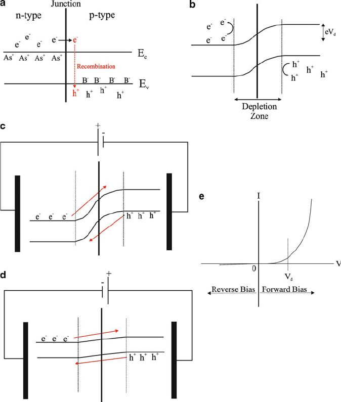
region, leaving behind positively charged n-dopant ions (e.g.,As
+
,P
+
). Likewise,
negatively charged p-dopant ions (e.g.,B
) are also formed on the p-Si side
(Figure 4.21a). Since the region in the vicinity of the p–n junction contains ions rather
than free electrons/holes, this is referred to as the depletion zone (Figure 4.21b).
The presence of oppositely charged ions within the depl etion region forms an
electric field (junction potential, eV
o
) that opposes, and eventually ceases, the
spontaneous movement of electrons/holes from their respective n- and p-type Si
regions. An external voltage may be applied that causes further band bending within
the depletion zone, referred to as reverse bias (Figure 4.21c). This will increase eV
o
,
making it harder to push electrons and holes toward the junction, which results in
little/no current.
[10]
However, if an external voltage is applied in the opposite
direction (forward bias), electrons and holes may easily diffuse across the p–n
junction (Figure 4.21d).
[11]
This electrically induced flow of electrons in only one
direction is referred to as a diode (Figure 4.21e ).
If a current is introduced to a simple configuration containing islands of n- or
p-type Si within a matrix of an oppositely doped Si substrate (i.e., p- or n-type Si,
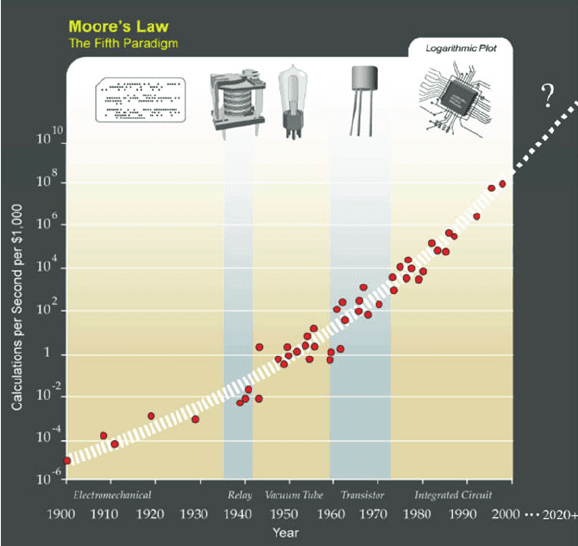
Figure 4.20. Upholding Moore’s Law through developments in computational paradigms. Adapted with
permission from the Wikipedia Creative Commons, Attribution License v.1.0 (Courtesy of Kurzweil
Technologies, Inc – http://www.kurzweilai.net/).
258 4 Semiconductors
respectively – Figure 4.22a), no electron flow will occur. This is because there is no
conduit between the electron-rich and electron-deficient regions. Electron flow will
occur if a metal is allowed to contact the doped-Si regions (Figure 4.22b); however,
there will be no control over the electrical current (analogous to the flow of water
Figure 4.21. Schematic of carrier flow within a p–n junction. Shown are (a) the diffusion of free electrons
from n- to p-type Si resulting in recombination with holes, (b) formation of a depletion zone that repels the
flow of electrons and holes from n- and p-type regions, respectively, (c) application of a reverse bias,
resulting in widening the junction potential, eV
o
, (d) application of a forward bias, which lowers eV
o
and
results in an exponential voltage spike once a threshold bias of V
D
is applied, (e).
4.2. Silicon-Based Applications 259
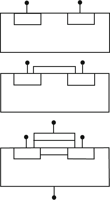
through a fully opened water faucet). Hence, the most effective arrangement that
will allow for controllable electrical conductivity is shown in Figure 4.22c. This
architecture allows one to control the electron flow through a gate by varying the
magnitude of the applied external voltage on the metal (or polysilicon – the modern
composition of complementary metal-oxide-semiconductor (CMOS) gates). Such a
configuration is known as a metal oxide semiconductor field-effect transistor
(MOSFET), where an insulating layer known as the gate oxide is used to prevent
uncontrollable tunneling of electrons between the gate and doped-Si substrate. The
term “field effect” refers to using an elect rical field to control the flow of electrons or
positively charged holes.
a
b
c
n-type Si n-type Si
p-type Si
n-type Si
n-type Si
n-type Si
n-type Si
n-type Si
P-type Si
(drain)
(Source)
metal
metal (gate)
gate oxide
channel
Figure 4.22. Schematic of possible n–p transistor architectures. Shown are: (a) n–p junction not capable
of transporting an electrical current, (b) metallic connectivity between electron-rich reservoirs, and (c) an
n-channel MOSFET, which features controllable electrical conductivity.
260 4 Semiconductors
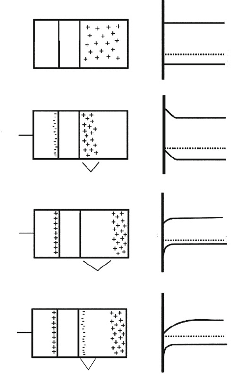
Let us now consider how an electrical charge may be controlled using a MO SFET.
To simplify the discussion, we will first consider a metal-on-semiconductor (nMOS)
capacitor – an nMOSFET without source and drain contacts (Figure 4.23a). When a
negative bias is applied to the gate (V
gate
), the positive holes are attracted from the
Metal
(gate)
Metal
(gate)
Metal
(gate)
Metal
(gate)
SiO
2
SiO
2
SiO
2
SiO
2
SiO
2
SiO
2
SiO
2
SiO
2
V
gate
V
gate
V
gate
p-type Si
p-type Si
p-type Si
p-type Si
p-type Si
Accumulation
Layer
Depletion
Region
Generated
Carriers
E
C
E
F
E
V
E
C
E
F
E
C
E
F
E
V
E
C
E
F
E
V
E
V
a
b
c
d
Figure 4.23. Charge distributions (left) and band diagrams (right) for an n-type metal-oxide-
semiconductor (nMOS) capacitor, with different gate bias modes. Shown are: (a) V
gate
¼ V
FB
, (b)
accumulation (V
gate
< V
FB
), (c) depletion (V
FB
< V
gate
< V
T
), and (d) inversion (V
T
< V
gate
). V
T
and
V
FB
are threshold and flat-band voltages, respectively. The flat-band voltage is obtained when the applied
gate voltage equals the work function difference between the gate and the semiconductor.
4.2. Silicon-Based Applications 261
substrate, forming an accumulation layer of positive charge on the SiO
2
/Si interface
(Figure 4.23b). The increase in hole concentration on the Si surface causes the
conduction and valence bands to bend upward, increasing the gap between the Fermi
level and conduction band.
By comparison, if a positive bias is applied to the gate, the positive holes will be
repelled from the SiO
2
/Si interface leaving behind a depleted region (Figure 4.23c).
Since the number of holes and electrons is constant, the electron concentration
increases near the silicon surface resulting in a downward bending of the conduction
and valence bands (i.e., narrowing the gap between E
F
and E
c
). Howeve r, for p-type
silicon, the electron density is negligible for small positive biases. As a result, the
gate charges are balanced not by electrons, but by negative acceptor ions (e.g.,B
)
in the depl etion layer. An increase in the gate bias causes the depletion layer to
widen, yielding more acceptor ions in order to balance the gate charge. The degree
of E
c
and E
v
band bending is directly related to the intensity of the positive gate bias.
At large positive gate biases, an inversion layer will form from the conduction band
lying closer to the Fermi level than E
v
. That is, at large applied voltages the surface
of the Si is inverted from p-type to n-type due to the generation of free electrons that
form a channel. In a MOSFET, the inversion-induced channel is located between the
source and drain. Accordingly, there are two types of MOSFETs: n-channel (NMOS
or nMOSFET) and p-channel (PMOS or pMOSFET), where the substrate comprises
p- and n-type silicon, respectively.
It should be noted that early MOSFETs used metallic gates; however, current
chips use polysilicon since it is chemically identical to the underlying substrate.
An advantage of polysilic on gates is a much smaller threshold voltage, V
t
,defined
as the gate voltage necessary to induce inversion in the channel region of the
substrate. The V
t
isrelatedtothedifferenceinthework function ( i.e., ’ –the
energy required to remove an electron from the surface of a material) between
the gate and channel regions. The threshold voltage is e spe c ially relevant for
current nanoscopic transistors, which utilize significantly lower applied voltages
relative to early MO SFETs. That is, as V
t
is reduced a weak inversion layer is
formed even when V
gate
¼ 0. This problem is referred to as sub-threshold leakage;
when magnified over a billion transistors, r esults in a large power di ssipation of a
modern-day chip.
Nevertheless, the miniaturization of MOSFETs is desirable for a number of
reasons. Most obviously, smaller transistors may be more densely packed on ICs.
The shrinking dimensions of individual transistors will shorten the distance from
source–drain, resulting in higher computational speeds. The high density of transis-
tors per chip is also essential to maintaining affordable ICs, since the cost of their
fabrication is directly related to the number of chips that may be contained on each
wafer. In addition to the density advantage, there is a significant operational benefit
of smaller MOSFETs. Since transistors may be considered as resistors in the on-
state, a smaller transistor will have less electrical resistance as well as lower gate
capacitance, allowing more current to pass through in a shorter period of time (i.e.,
262 4 Semiconductors
higher processing speeds and less power). Equation 6 shows the dependence of
various transistor properties to its observed current.
I
DS
¼
W
2Lt
ox
mCðV
GS
V
T
Þ
2
ð6Þ
Where I
DS
is the drain current; W, the channel width; L, the channel length; t
ox
, the
gate oxide thickness; m, the channel carrier mobility; C, the capacitance density of
the gate oxide; V
GS
, the gate vo ltage; and V
T
is the threshold voltage.
Perhaps the most crucial component of the transistor structure is the gate oxide,
which serves as the insulator between the gate and channel. Ideally, the oxide layer
should be as thin as possible to increase the channel conductivity when the transistor
is on, and reduce sub-threshold leakage when the transistor is off. Since the first
MOSFETs were demonstrated, the gate length has steadily decreased to a current
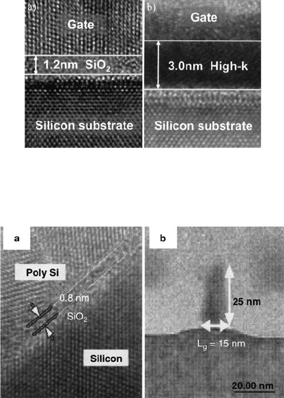
size of less than 30 nm (Figure 4.24). For the current “32 nm technology node,” this
translates to a gate oxide (likely comprised of hafnium oxide or silicate) thickness of
0.9 nm, or less than 5 atomic layers (Figure 4.25a). Incredibly, transistors with a
channel length of 15 nm and SiO
2
thickness of only 8 A
˚
have already been proven in
the laboratory (Fig ure 4.26); channel lengths less than 10 nm may be realized within
5 years! This represents an entire order of mag nitude decrease from only 30 years
ago, when the oxide layer thickness was ca. 100 nm.
Transistor Scaling
Transistor
Physical Gate
Length
Technology
Node
Nanotechnology
Nanometer
0.5µm
0.35µm
0.25µm
0.18µm
0.13µm
90nm
130nm
70nm
50nm
30nm
20nm
15nm
85nm
45nm
30nm
1.0
0.1
0.01
1990 1995 2000 2005 2010
10
100
1000
Micrometer
Year
Figure 4.24. Scaling of transistor size. The top line indicates the technology node, whereas the bottom
line indicates the physical size of the gate. It should be noted that the “technology node” no longer refers
to physical dimensions of the transistor, but is rather an industry term related to a new fabrication process
every 2 years, in accord with Moore’s Law. By definition, the technology node refers to half the distance
(half-pitch) between cells in a DRAM memory chip. It is noteworthy that the gate length, L, officially
moved into the nanoregime in the year 2000. Reproduced with permission from Intel Corporation (http://
www.intel.com).
4.2. Silicon-Based Applications 263
As one can imagine, such a thin insulating layer is prone to electron tunneling
between the polysilicon gate and channel, leading to increased power consumption
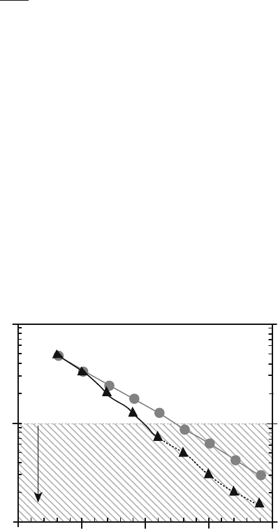
and heat buildup. Current transistors exhibit a relatively high leakage current
density, on the order of 1–10 A cm
2
(Figure 4.27). Empirical and theoretical
studies have shown that the practical limit for dielectric effectiveness of the gate
SiO
2
layer is ca. 0.7–1 nm. It should also be noted that as the oxide thickness
Figure 4.25. Cross-section high-resolution transmission electron microscopy (HRTEM) images of gate
oxides for MOSFETs. Provided is an illustration of film thicknesses that result in identical capacitance for
SiO
2
(k ¼ 3.8), relative to a high-k dielectric (k ¼ 23.9) gate oxide. Hence, increased gate capacitance
will result from thinner films comprising high-k dielectric materials. Reproduced with permission from
Intel Corporation (http://www.intel.com).
Figure 4.26. Cross-section HRTEM images of next-generation MOSFET gates. Reproduced with
permission from Intel Corporation (http://www.intel.com).
264 4 Semiconductors
decreases, other issues arise such as boron diffusion into the channel. This would
significantly alter the threshold voltage, and ultimate drain current, of the transistor.
In cont rast to the high-performance microprocessor market, the rapidly growing
market of low-power applications requires transistors with much lower leakage
currents (ca.10
3
Acm
2
). One intriguing strategy that has been proposed by
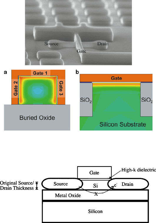
Intel to minimize off-state leakage current is the design of nonplanar tri-gate
transistors (Figure 4.28).
[12]
Since electrical signals must move up and over the
vertical gate, the effective pathway for electrical current transmission is tripled
relative to today’s planar MOSFETs (Figure 4.28a, b). Further on the horizon, this
problem will be circumvented through the use of entirely new paradigms (e.g.,
ballistic deflection transistors
[13]
) that employ a variety of nanoarchitectures, as
we continue to push Moore’s Law to higher limits.
Key features of next-generation designs that will help reduce gate and source/drain
leakage include the use of an alternate gate oxide (see below), a silicon-on-insulator
(SOI) substrate, and raised source/drain regions (Figure 4.29). The purpose of introdu-
cing source and drain cavities with greater thicknesses is rather intuitive. The electrons
will have more room to maneuver, resulting in less electron–electron repulsions and
lower overall resistance. This translates to a lower operating voltage for the transistor,
which results in low power consumption with less heat generation during its operation.
The presence of an insulating layer directly beneath a thin Si channel is reported
to reduce off-state leakage from source to drain regions by more than two orders of
magnitude.
[14]
When the top of the buried oxide layer (BO
x
) coincides with the
bottom of source/drain, the architecture is referred to as a fully depleted SOI; a small
interfacial gap is known as partially depleted SOI, and will result in greater off-state
leakage current. Since depleted substrates feature a nonconductive barrier, the
Figure 4.27. The trend of increasing leakage current density with decreasing gate length. Reproduced
with permission from Intel Corporation (http://www.intel.com).
4.2. Silicon-Based Applications 265
transistor is able to swit ch on/off faster due to more effective drive current while in
the on-state.
Another improvement to the transistor design that addresses gate leakage problems
is the replacement of the SiO
2
gate oxide with insulating films known as high-k
dielectrics,wherek refers to its dielectric constant (Figure 4.25).
[15]
These materials
have a larger dielectric constant than commonly used SiO
2
(k ¼ 3.82), which allows
one t o use thicker oxide layers for an identical gate capacitance (Eq. 7):
Figure 4.28. SEM image of a nonplanar tri-gate transistors. Also shown is the enhanced electron flow
(shown in red) of (a) tri-gate, relative to (b) standard planar MOSFETs. Reproduced with permission from
Intel Corporation (http://www.intel.com).
Figure 4.29. Cross-section schematic of an advanced transistor design. Features illustrated are: (a) raised
source and drain contacts, (b) an SOI substrate that prevents off-state leakage from source to drain, and
(c) a high-k dielectric gate insulator. These three components employed in tandem are the basis of a faster
generation of transistors referred to as “terahertz transistors.”
266 4 Semiconductors
C
vol
/
k
t
2
ð7Þ
Where C
vol
is the capacitance per unit volume; k, the dielec tric constant (or, relative
permittivity); and t is the thickness of the dielectric medium.
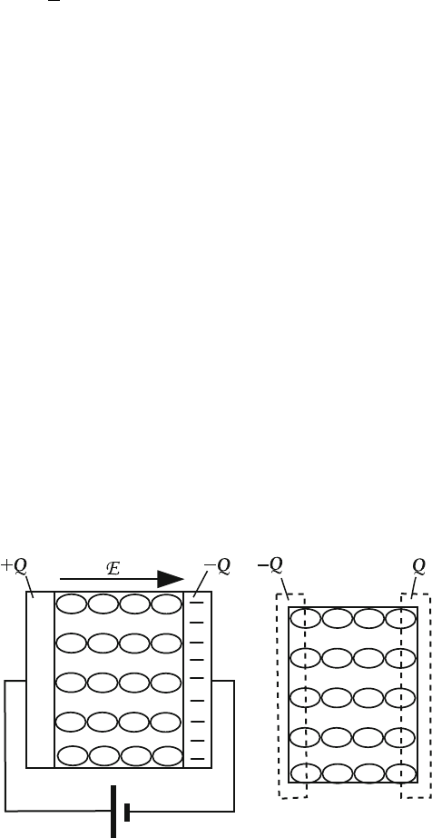
Materials that exhibit a high dielectric constant are strongly polarizable. That is,
when exposed to an electric field, the dipole moments of the constituen t molecules
and atoms of the dielectric material will become aligned. This results in the buildup
of electrical charges on the surface of the capacitor plates (Figure 4.30). In general,
inorganic materials with ionic or partial ionic interactions will possess a relatively
large dielectric constant (high-k), whereas organic molecules with nonpolar bonds
are typically low-k materials. Materials containing relatively large atoms will be
most useful as dielectrics, since they exhibit greater polarizabilities due to valence
electrons being situated farther from the nucleus.
In addition to being polarizable, it is also paramou nt that the dielectric medium be
of low conductivity (i.e., have a large bandgap – an offset with Si of >1 eV), to
minimize carrier injection into its bands. For example, although the dielectric
constants for Ta
2
O
5
and TiO
2
are sufficiently large for high-k gate oxide applica-
tions (see below), both of these materials have small bandgaps (4.5 and 3.5 eV;
relative to 8.9 eV for SiO
2
), which will result in high leakage currents. On the other
hand, more promising candidates include Al
2
O
3
, HfO
2
, and ZrO
2
, with bandgaps of
8.7, 5.7, and 7.8 eV, respectively. Other properties that must be inherent in the high-
k dielectric layer include thermodynamic and kinetic stabilities with the Si channel
Bound polarization
charges on the surfaces
P
P
+
-
+
-
+
-
+
-
+
-
+
-
+
-
+
-
+
-
+
-
+
-
+
-
+
-
+
-
+
-
+
-
+
-
+
-
+
-
+
-
+
-
+
-
+
-
+
-
+
-
+
-
+
-
+
-
+
-
+
-
+
-
+
-
+
-
+
-
+
-
+
-
+
-
+
-
+
-
+
-
+
+
+
+
+
+
+
+
+
+
V
Figure 4.30. Schematic of bound polarization occurring on capacitor plates due to polarization of the
dielectric medium. Reproduced with permission from Kasap, S. O. Principles of Electronic Materials and
Devices, 2nd ed., McGraw-Hill: New York, 2002.
4.2. Silicon-Based Applications 267