Fahlman B.D. Materials Chemistry
Подождите немного. Документ загружается.

and polysilicon gate (e.g., no silicide formation, especially under high-temperature
processing conditions), and little/no electrically active defect sites.
The longevity of the dielectric material is dependent on the exposed voltage.
When too high a voltage is introduced between the electrodes, dielectric breakdown
of the solid may ensue. The solid-state structure, presence of impurities or
microstructural defects (e.g., cracks/voids), and ambient conditions (e.g., temperature,
humidity) are all paramount in assessing the dielectric strength (i.e., resistance to
breakdown) of an insulating material. As you might imagine, these factors become
even more relevant when considering the 0.8–1 nm SiO
2
layers found in modern
MOSFETs.
There are three types of high-k dielectrics (measured dielectric constants in
parentheses):
1. Materials with 4 < k < 10 (i.e., relatively weak polarizability) such as: Al
2
O
3
(7.5–10), Si
3
N
4
(7.9–8.1), sodalime glass (7.2), Al
6
Si
2
O
13
(mullite, 6.3),
MgAl
2
O
4
(spinel, 8.6), MgSiO
4
(forsterite, 6.2), MgO (9.65), ZnO (8.15), BN
(4.15), BeO (6.8), CaF
2
(6.8), BaCO
3
(8.5), SrCO
3
(8.85), (KAl[Si
3
O
10
(OH)
2
])
(mica muscovite, 6.5–8.7) , and organic polymers (polyurethane: 7.1, polyvinyl
fluoride: 7.4, polyvinylidene fluoride: 6.4).
2. Materials with 10 < k < 100 such as: MnO
2
(pyrolussite, 12.8), ThO
2
(18.9),
Ta
2
O
5
(27.6), UO
2
(24), Nb
2
O
5
(67), HfO
2
(25), ZrO
2
(12.5–24.7), Zr
x
Hf
1x
O
2
(25), Y
2
O
3
(15), La
2
O
3
(25), Gd
2
O
3
(23), Pr
2
O
3
(25), and BaZrO
3
(43).
3. Materials with k > 100 (i.e., strongl y polarizable) such as: TiO
2
(rutile, 85–170),
PbZrO
3
(200), Pb(Zr
0.52
Ti
0.48
)O
3
(“PZT,” 1,800), SrTiO
3
(2,080), Ba
(Sr
0.52
Ti
0.48
)O
3
(3,000), Pb(Ni
0.33
Nb
0.67
)O
3
(5,500), and BaTiO
3
(6,000).
Silicon (oxy)nitride dielectrics were touted as the near-term alternative for SiO
2
;
however, these have been largely eclipsed by HfO
2
-based films. Though Si nitrides/
oxynitrides would result in only a marginal increase in the dielectric constant
relative to other high-k candidates, the attract iveness of these films is related to
their mature deposition techniques, and more desirable electronic barrier properties
(i.e., reduced boron diffusion). Not unlike its SiO
2
predecessor, Si
3
N
4
films reach
a functional limit of 1.2 nm; hence, there is ongoing research for the development
of alternative gate oxide materials (and com patible gate stacks – for example,
polysilicon gates are not suitable for ZrO
2
and HfO
2
) that will be useful in the
long-term to keep pace with ensuing transistor improvements.
Two factors are responsible for increasing the speed of transistor switching – the
channel length between source and drain, and the speed of elect ron transport through
the channel. Since it is becoming increasingly more difficult to shrink MOSFET
dimensions, materials scientists are searching for new ways to address the latter
consideration. In 2002, Intel first reported the use of “strained Si” in their 90 nm
technology node, in which the silicon lattice in the channel region is strained through
compression or expansion. It h as been shown that electrons flow through strained
silicon 70% faster than in unstrained silicon. For ICs, this translates to a 17%
increase in speed at the same powe r, or 35% reduction in power consumption at
the same speed.
[16]
268 4 Semiconductors
To under stand this effect, we need to consider the Si–Si bonding within the bulk
crystalline solid. As we discussed earlier, electrons are promoted from valence to
conduction bands due to thermal excitation. The valence band of the extended solid
is formed from the overlap of sp
3
hybridized orbitals residing on each Si atom. When
an electron migrates from valence to conduction bands under normal circumstances,
there is no directional preference. However, when a strain is introduced along a
specific direction of the lattice, the ener gies of the hybrid orbitals along this direction
are altered.
A stret ching, or tensile, strain will cause the orbitals between neighbori ng Si
atoms to be expanded that weakens Si–Si bonds along the strain direction. Hence,
it becomes easier for an electron to be thermally promoted from the valence to
conduction band, corresponding to greater electron mobility. This effect is more
pronounced for n-channel MOSFETs; the strain-expanded hybrid orbitals between
neighboring Si atoms are able to accept electron density with less electron repulsion.
By contrast, compressive strain is typically used for p-channel MOSFETs, where the
presence of holes is able to offset the electron–electron repulsion within the com-
pressed hybrid orbitals. More simplistically, crystal strain increases the free mean
path of electrons (i.e., less scattering through electron–lattice interactions), which
increase their velocity under a given field.
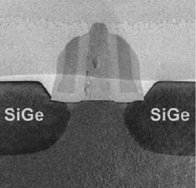
Compression strain of p-doped Si is most often accomplished by carving trenches
on opposite ends, and filling these with a material with greater lattice spacing than
Si. This is typically a material such as Si
1x
Ge
x
(x ¼ 0.1–0.3) solid solutions
(Figure 4.31); since the lattice constants of Si and Ge are 5.43 and 5.66 A
˚
,
Figure 4.31. Cross-section HRTEM image of a transistor containing a compression-strained channel.
Reproduced with permission from Intel Corporation (http://www.intel.com/research/downloads/Strained-
Si-paper-IEDM-1203.pdf).
4.2. Silicon-Based Applications 269
respectively, the lattice const ant of the solution is [5.43(1 x) + 5.66x A
˚
].
A common method used to induce tensile strain is the deposition of a dense ceramic
Si
3
N
4
film on top of the channel. Both of these methods result in uniaxial strain,
which is preferred since localized regions may be altered rather than the entire
wafer. In fact, these techniques may be used to modify both nMOSFETs and
pMOSFETs on a single chip. By contrast, biaxial strain is induced through the
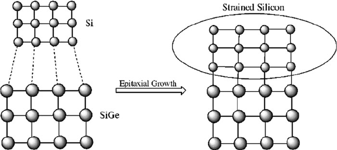
heteroepitaxial deposition of a Si thin film on top of a SiGe substrate (Figure 4.32).
A number of prec ursors such as germane (GeH
4
; 400–700
C dep. T), germanium
tetrachloride (GeCl
4
; >850
C dep. T), isobutylgermane (C
4
H
9
GeH
3
; 400–500
C
dep. T) and methylgermanium chloride ((CH
3
)GeCl
3
; 750–1,000
C dep. T) may be
used to deposit the SiGe base layer using chemical vapor deposition (a technique
described in more detail later in this chapter). The amount of strain and mobility
enhancement depends on the germanium content of the SiGe layer.
Integrated circuit fabrication
From the dawn of civilization, no other field has progressed as rapidly as
microelectronics. Gordon Moore, an integrated circuit pioneer and co-founder of
Intel stated (in 1998): “If the auto industry advanc ed as rapidly as the semiconductor
industry, a Rolls Royce would get a half a million miles per gallon, and it would be
cheaper to throw it away than to park it.” The computers we purchase today are
almost immediately out-dated, due to constant improvements of microprocessor
speeds and memory/storage abiliti es. A tiny integrated circuit (IC) lies beneath the
protective packaging material of virtually any modern electronic device, acting as its
nerve center. Like any other advanced technology, we take these feats of modern
engineering for granted. Beneath the familiar black plastic casing of a computer chip
are billions of complex transistor subunits, along with additional components and
circuitry, to offer precise control over the flow of electrons.
Figure 4.32. Formation of strained silicon from the epitaxial growth of lattice mismatched Si onto a SiGe
substrate.
270 4 Semiconductors
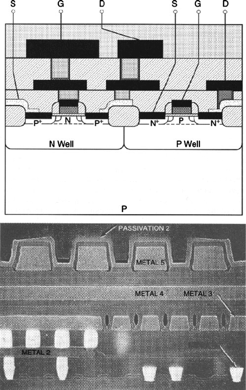
The major class of digital ICs is the CMOS. The most familiar CMOS applications
include microprocessor and RAM chips. As its name implies, CMOS technology
involves the complimentary operation of interconnected nMOSFET and pMOSFET
pairs (Figure 4.33). Relative to NMOS or PMOS integrated circuitry, CMOS is the
design-of-choice for the majority of ICs due to distinct advantages in overall design
simplicity and reduction in power.
Figure 4.33. Cross-section illustration and SEM image of an integrated circuit. Reproduced with
permission from Plummer, J. D.; Deal, M. D.; Griffin, P. B. Silicon VLSI Technology, Prentice-Hall:
New York, 2000. SEM image Courtesy of Chipworks, Inc., Ottawa, Ontario, Canada.
4.2. Silicon-Based Applications 271
There has also been an increased interest in SOI chips,
[17]
comprising transistors
in which a thin insulating layer lies between a thin layer of Si (in the channel region)
and the bulk Si substrate (revisit Figure 4.29). This tec hnology is not new; in fact,
SOI ICs have been used sinc e the 1960s for military and space applications. As the
relatively high cost of production continues to decrease, SOI substrates will
undoubtedly be important for CMOS ICs within future commercial electronic
devices. The insulation between source and drai n cavi ties allows the threshold
voltage (also decreasing the supply voltage) of the SOI CMOS device to be
extremely low, with minimal off-state (i.e., sub-threshold) leakage. It is reported
that this simple substrate alteration results in chips that operate more than 30%
faster, and use ca. 20% less power than standard CMOS analogs. The use of less
power per chip is important for extending the battery life of portable electronics, as
well as dealing with the heat generated by ICs. If one extrapolates the enormous heat
generated from high-density bulk Si chips into the near-future, it may be necessary
to use liquid coolants within the IC package – clearly not a desirable (or feasible)
option.
Without question, the fabrication of modern ICs from grains of sand is one of the
greatest feats ever accomplished. More than 300 carefully designed processing steps
are used to form a dense packing of nanoscale objects onto a thin wafer of silicon.
The silicon wafers u sed for IC fabrication are obtaine d through precise slicing of
high-purity ingots using a diamond saw. Th e wafer edges are ground to a round
finish polished until they have a defect-free mirrored finish. In order to reduce the
cost/transistor, there has been a shift to larger wafers that may hold a greater number
of ICs – from diameters of 200 to 300 mm (i.e.,12
00
). Should a SOI substrate be
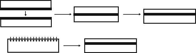
desired, two methods are typically used for its fabrication (Figure 4.34). A bulk Si
wafer may be exposed to high-energy beam of oxygen ions that diffuse below the
surface. Also, two wafers – a bulk Si and one coated with a SiO
2
film (or two
oxidized wafers) – are bonded together using specialized techniques.
Whether the substrate is bulk Si or SOI, the most critical step in IC fabrication is
the initial cleaning of the wafer. The RCA clean procedure is the industry standard,
Si
Si
Si
a
b
SOI
SOI
O ion implantation
Thermal
Annealing
Excess Si
Removal
SiO
2
SiO
2
Figure 4.34. Two methods used to fabricate silicon-on-insulator (SOI) wafers. Illustrated are the (a)
Smartcut procedure where two oxidized wafers are bonded together and (b) SIMOX procedure where
oxygen ions are implanted into a bulk Si wafer.
272 4 Semiconductors
consisting of the following complex treatment to remove both organ ic and inorganic
contaminants. It should be noted that these procedures are perf ormed within a clean
room, to avoid particulate contamination:
(i) SC-1 clean
– The wafer is degreased using acetone, isopropyl alcohol, and ultrapure water
(UPW) rinses.
– The native SiO
2
layer is removed from the surface by exposing the wafer to
a 50:1 UPW:HF solution for 30 s, followed by a prolonged UPW rinse.
– The wafer is exposed to a 10:2:1 DIW:H
2
O
2
:NH
4
OH solu tion at 75
C for
10 min, followed by a final UPW rinse. This effectively removes particulate
contamination from the surface.
– nitrile gloves and Teflon tweezers are used to handle the wafer during
treatments.
(ii) SC-2 clean
– Remaining surface oxides and hydroxides are removed by exposing the wafer
to a 50:1 UPW:HF etching solution for 15 s, followed by a prolonged UPW
rinse.
– The wafer is exposed to a 10:2:1 UPW:H
2
O
2
:H
2
SO
4
solution at 75
C,
followed by a UPW rinse. This effectively removes metals/ions from the
surface.
– The wafer is rinsed with DIW for ca. 20 min., followed by drying under N
2
flow.
– When finished, the polished wafer surface should be reflective with no
observable residues.
Since we are considering the starting wafer, it should be noted that often the
substrate consists of an epitaxially grown doped Si film on the surface of a more
heavily doped bulk Si wafer. If the film is of the same composition of the underlying
substrate, this process is referred to as homoepitaxy, or simply epi. By contrast,
heteroepitaxy refers to a Si film grown onto a different substrate such as sapphire
(a-alumina). Using epi wafer substrates is generally more expensive than bulk
analogues, but offers the advantage of fine-tuning the conductivity of the channel
region for optimal operation of the CMOS IC. Through careful film deposition
methodology, it is also possible to eliminate O and C impurities resulting in further
improvements in device performance.
It should be noted that there are benefits of using GaAs instead of Si for IC
applications such as:
(i) Faster discrete components and ICs due to a larger low-field electron mobility
(9,200 vs. 1,600 cm
2
V
1
s
1
, respectively) and lower saturation field
(ii) The bandgap of GaAs is greater than Si (1.4 eV vs. 1.12 eV, respectively),
which results in semi-insulating properties and reduced parasitic capacitance
(iii) Direct bandgap properties results in light emission for laser, LED, and micro-
wave emitters for cellular phone applications.
However, GaAs has not been able to replace Si for microelectronic applications
since Ga and As have much lower natural abundances, and As has a high toxicity.
4.2. Silicon-Based Applications 273
In addition, no native oxide forms on GaAs, which increases the complexity and cost
of production. Lastly, GaAs has a much lower thermal conductivity relative to Si,
resulting in lower packing densities at a time when Moore’s Law demands signifi-
cant increases. Germanium and other III–V such as InP, InAs, or InSb have also been
suggested to replace Si in future technology nodes due to their higher electron
mobilities (3,900, 5,400, 40,000, and 77,000 cm
2
V
1
s
1
, respectively) , of interest
for nMOS devi ce applications. Germanium also has a very high hole mobility
(1,900 cm
2
V
1
s
1
vs. 430 (Si), 400 (G aAs), 200 (InP), 500 (InAs), and 850
(InSb)), which could be useful for pMOS devices.
[18]
A substrate candidate that is used for high-speed optical networking and inexpen-
sive, lightweight personal communication devices is SiGe (“siggie”). Whereas Si
does not operate at frequencies above a few GHz, SiGe semiconductors have speeds
up to 120 GHz, which increases current speeds by up to a factor of four.
[19]
The
added processing cost will not result in the replacement of Si for CMOS applica-
tions; however, SiGe might replace III–V semiconductors (e.g., InP, GaAs) for niche
future applications such as watch-size cellular phones, collision-avoidance radar
systems, wireless ICs, and low-power radio-frequency (RF) chips.
Regardless of bulk Si, epi, or SOI subst rates, a key consideration that is para-
mount toward subsequent processing steps is the crystal orientation employed.
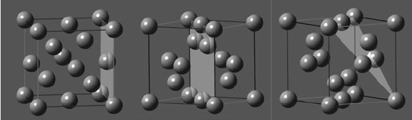
Three important crystal planes for silicon include Si(100), Si(110), and Si(111) –
Figure 4.35. The surface atomic densities increase in the order Si(100) < Si(110)
< Si(111). Empirically, this translates to available Si–Si bond densities of
6.77 10
14
, 9.59 10
14
, and 11.76 10
14
cm
2
, respectively.
[20]
Hence, the
rates required to remove (etch), or react with, surface atoms (e.g., thin-film deposi-
tion) should follow the reverse order as above. However, the Si(110) orientation
etches fastest due to its more corrugated structure, relative to the other atomically
flat surfaces (Figure 4.36). To illustrate this effect, exposure of a wafer to a 40%
alcoholic KOH solution results in Si etching at rates of 13,000, 6,000, and 90 A
˚
min
1
, for the Si(110), Si(100), and Si(1 11) planes, respectively.
Since bonds are broke n during Si wafer formation from the bulk ingot, atoms at
the surface will have a lower coordination number, resulting in a higher surface
energy and greater reactivity (Figure 4.37). One way to remove these surface defects
is through passivation. For example, a large number of dangling bonds are tied up
Figure 4.35. Unit cell representations of silicon showing the (100), (110), and (111) planes, respectively.
274 4 Semiconductors
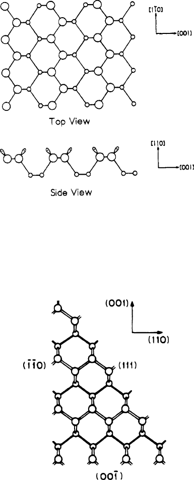
Figure 4.37. Dangling bond formation on reconstructed surfaces of (110), (111), and (100) planes of Si.
The sizes of silicon atoms are shown to decrease away from the page. Reproduced with permission from
Waltenburg, H. N.; Yates, J. T. Chem. Rev. 1995, 95. Copyright 1995 American Chemical Society.
Figure 4.36. Top and side views of the unreconstructed Si (110) surface. Each of the upper surface atoms
has one dangling bond, as illustrated in the side view. Reproduced with permission from Waltenburg, H.
N.; Yates, J. T. Chem. Rev. 1995, 95. Copyright 1995 American Chemical Society.
4.2. Silicon-Based Applications 275
by H atoms during HF etching to remove native SiO
2
(the RCA clean procedure
above). The unfavorable positive free energy of the surface may also be minimized
by using solid surfaces with a high atomic density (i.e., stability: Si(111) >
Si(110) > Si(100)).
Neighboring unsaturated Si atoms may also self-assemble in a number of ways,
referred to as surface recon struction, which minimizes the overall energy of the
surface. For instance, the formation of a Si(100) surface leaves two dangling bonds
per surface Si atom; dimerization reduces the coordinative unsaturation by 50%
(Figure 4.38a). A much more complex multi-step reconstruction for annealed
Si(111) surfaces may also be observed directly by scanning tunneling micro-
scopy (STM, Figure 4.38b).
[21]
In addition to reconstructed surfaces, native surfaces
that contain adsorbates are also denoted by the Woods notation (Figure 4.38c),
which provides the crystal orientation of the surface, along with the dimensions/
alignment of the adsorbate units in comparison to the underlying bulk substrate.
[22]
For instance, a nitrogen atom adsorbed onto a 2 2 reconstructed Cu(100) surface
would be designated as:
Cu ð100Þ c ð2x2ÞN
substrate plane centering meshratio adsorbate
The fabrication of a CMOS IC involves a repeating sequence of film deposition,
patterning, and dopant implantation procedures (Figure 4.39 ). The initial step
involves the deposit ion of SiO
2
onto the wafer surface. You may be wondering
why this is necessary, since the cleaning procedures were designed to remove the
native silica layer. However, this procedure involves the controlled deposition of an
amorphous SiO
2
coating of known thickness onto the wafer surface.
[23]
By defini-
tion, such a coating is referred to as a thin film, since its thickness is less than 1 mm.
Two reactions are responsible for the formation of SiO
2
(Eqs. 8 and 9; dry and wet
oxidation, respectively). A variety of factors gover n the resultant thickness of the
silica film, such as temperature and pressure/flowrate of O
2
.
Si + O
2
!
7001200
c
SiO
2
ð8Þ
Si + 2 H
2
O !
1100
c
SiO
2
þ2H
2
ð9Þ
It should be noted that SiO
2
deposition does not occur through simple addition to
the wafer surface. Rather, as the surface becomes oxidized, oxygen atoms are also
able to diffuse from the surface to react with underlying Si atoms. The incoming O
2
or H
2
O molecu les adsorb dissociatively to the Si surface, resulting in the O/OH
groups being either attached to dangling Si bonds, or inserted between Si–Si bonds
of the same layer. As the temperature is increased, there is a greater degree of
oxygen insertion into Si–Si bonds of underlying layers, which adds to the thickness
of the SiO
2
film.
276 4 Semiconductors
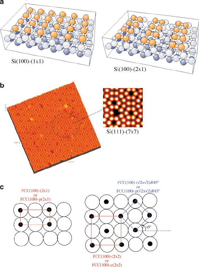
Figure 4.38. Surface reconstruction of Si planes. Shown are a) fcc-(100)-(2 2), also referred to as fcc-
(100)-p(2 2) referring to a primitive unit, b) an STM image of a Si(111) reconstructed surface, and
c) the Woods notation of reconstructed fcc(100) surfaces.
4.2. Silicon-Based Applications 277