Endo M., Iijima S., Dresselhaus M.S. (eds.) Carbon nanotubes
Подождите немного. Документ загружается.

58
C.-H. KI
C. Colliex, and J.
M.
Planeix,
Chern. Phys. Lett.
215,
509 (1993).
5.
C.-H. Kiang, W.
A.
Goddard
111,
R. Beyers, J. R. Sa-
lem, and D.
S.
Bethune,
J.
Phys. chem.
98,6612 (1994).
6.
C.-H. Kiang,
P.
H.
M.
van Loosdrecht, R. Beyers, J. R.
Salem, D.
S.
Bethune, W. A. Goddard
111,
H.
C.
Dorn,
P.
Burbank, and
S.
Stevenson,
Proceedings
of
the Sev-
enth Internutional Symposium
on
Small Particles und
Inorganic Clusters,
Kobe, Japan,
Surf. Rev. Lett.
(in
press).
7. S.
Seraphin and D.
Zhou,
Appl. Phys. Lett.
64, 2087
(1994).
8. S.
Seraphin,
J.
Electrochem.
SOC.
(USA)
142,290 (1995).
9.
S. Seraphin,
D.
Zhou, J.
Jiao,
M.
S.
Minke,
S.
Wang,
T.
Yadav, and
J.
C.
Withers,
Chem. Phys. Lett.
217,
191
(1 994).
10.
Y.
Tapesh, J. C. Withers,
S.
Seraphin,
S.
Wang, and D.
Zhou, In
NovelForms
of
Carbon,
MRS Proc.
349,
pp.
275-281.
Mat. Res. SOC., Pittsburgh
(1994).
11.
J.
M. Lambert,
P.
M.
Ajayan,
P.
Bernier, J. M. Planeix,
V. Brotons,
B.
Cog, and J. Castaing,
Chem. Phys. Lett.
226,
364 (1994).
12.
S. Subramoney, R.
S.
Ruoff, D. C. Lorents, and R. Mal-
hotra,
Nature
366, 637 (1994).
13.
S.
Wang and D. Zhou,
Chem. Phys. Lett.
225, 165
(1994).
14.
D. Zhou,
S.
Seraphin, and
S.
Wang,
Appl. Phys. Lett.
65, 1593 (1994).
15.
S.
Subramoney,
P.
van Kavelaar, R.
S.
Ruoff, D.
C.
Lorents, and
A.
J.
Kazmer, In
Recent Advances in the
Chemistry and Physics
of
Fullerenes and Related Mate-
rials
(Edited by K.
M.
Kadish and
R.
S. Ruoff). The
Electrochemical Society, Pennington, NJ
(1994).
16.
Y.
Saito, T. Yoshikawa,
M.
Okuda, N. Fujirnoto, K.
Sumiyama, K. Suzuki,
A.
Kasuya, and
Y.
Nishina,
J.
Phys. Chern.
Solids
54, 1849 (1993).
17.
Y. Saito, M. Okuda, N. Fujimoto,
T.
Yoshikawa,
MI.
Tomita,
and
T.
Hayashi,
Jpn.
J.
Appl. Phys.
2
Lett.
(Ja-
pan)
33, L526 (1994).
18.
X.
Lin,
X.
K. Wang,
V.
P.
Dravid,
R.
P.
H.
Chang, and
5.
B. Ketterson,
Appl. Phys. Lett.
64, 181 (1994).
19.
M.
Endo,
K.
Takeuchi,
S.
Igarashi, K. Kobori,
M.
Shiraishi, and
H.
W.
Kroto,
J.
Phys. Chem. Solids
54,
1841 (1993).
20.
D. Ugarte,
Nature
359,
707 (1992).
21.
Y. Saito, T. Yoshikawa, M. Inagaki, M. Tomita, andT.
22.
R.
S.
Ruoff, J. Tersoff, D. C. Lorents, S. Subramoney,
23.
J.
Tersoff and R.
S.
Ruoff,
Phys. Rev. Lett.
73, 676
24.
M. Endo,
Chemtech
18, 568 (1988).
25.
N.
M.
Rodriguez,
J.
Mater. Res.
8, 3233 (1993).
26.
R. Saito, M. Fujita, G. Dresselhaus, and M.
S.
Dressel-
haus,
Matls. Sci.
Eng.
B19, 185 (1993).
27.
P.
W.
Fowler,
J.
Phys. Chem. Solids
(UK)
54, 1825
(1993).
28.
R. Saito,
G.
Dresselhaus, and
M.
S.
Dresselhaus,
Chern.
Phys. Lett.
195, 537 (1992).
29.
S.
Iijima,
Mutls.
Sci.
Engin.
B19,
172 (1993).
30.
B.
I.
Dunlap,
Phys. Rev.
B
49, 5643 (1994).
31.
B.
I. Dunlap,
Phys. Rev.
B
50, 8134 (1994).
32.
B.
I.
Dunlap,
Phys. Rev.
B46,
1933 (1992).
Hayashi,
Chem. Phys. Lett.
204, 277 (1993).
and
B.
Chan,
Nature
364, 514 (1994).
(1
994).
ANG
et
al.
33.
L. A. Chernozatonskii,
Physics Lett. A
(Netherlands)
172, 173 (1992).
34.
J. W. Mintmire, D.
H.
Robertson, and C. T. White,
J.
Phys. Chern. Solids
54, 1835 (1993).
35.
R. Saito, M. Fujita, G. Dresselhaus, and
M.
S.
Dressel-
haus,
Phys. Rev.
B46, 1804 (1992).
36.
R. A. Jishi, M.
S.
Dresselhaus, and
G.
Dresselhaus,
Phys. Rev.
848, 11385 (1993).
37.
M.
S.
Dresselhaus,
G.
Dresselhaus, and R. Saito,
Solid
State
Commun.
(USA)
84, 201 (1992).
38.
R.
A. Jishi,
D.
Inomata,
K.
Nakao, M.
S.
Dresselhaus,
and
G.
Dresselhaus,
J.
Phys. Soc.
Jpn.
(Japan)
63,2252
(1994).
39.
N.
Hamada,
S.
I.
Sawada, and A. Oshiyama,
Phys. Rev.
Lett.
68, 1579 (1992).
40.
C.
J. Mei and
V.
H. Smith Jr.,
Physicu
C
213,
157
(1993).
41.
M.
Springborg and
S.
Satpathy,
Chem. Phys. Lett.
225,
454 (1994).
42.
R.
A.
Jishi and
M.
S.
Dresselhaus,
Phys. Rev.
B45,
11305 (1992).
43.
R. A Jishi, L. Venkataraman, M. S. Dresselhaus, and
G.
Dresselhaus,
Chem. Phys. Lett.
209,77 (1993).
44.
J. M. Holden,
P.
Zhou, X-x Bi,
P.
C. Eklund,
S.
Ban-
dow, R.
A.
Jishi,
K.
Das Chowdhury, G. Dresselhaus,
and
M.
S.
Dresselhaus,
Chem. Phys. Lett.
220, 186
(1994).
45.
R.
Kuzuo,
M.
Terauchi,
M.
Tanaka, and Y. Saito,
Jpn.
J.
Appl. Phys.
2,
Lett.
33,
L1316 (1994).
46.
M.
E.
McHenry,
S.
A. Majetich, J.
0.
Artman, M.
DeGraef, and
S.
W. Staley,
Phys. Rev.
B 49, 11358
(1 994).
47.
S.
A. Majetich,
J.
0.
Artman,
M.
E.
McHenry, N.
T.
Nuhfer, and
S.
W
Staley,
Phys. Rev.
B48, 16845 (1993).
48.
R.
S.
Ruoff, D. C. Lorents, B. Chan, R. Malhotra, and
S.
Subramoney,
Science
259, 346 (1993).
49.
Y. Saito,
T.
Yoshikawa,
M.
Okuda, M. Ohkohchi, M.
Inagaki, Y. Ando, A. Kasuya, and Y. Nishina,
Chern.
Phys. Lett.
209,
72 (1993).
50.
S.
Seraphin, D. Zhou, J. Jiao, J. C. Withers and
R.
Loutfy,
Appl. Phys. Lett.
(USA)
63, 2073 (1993).
51.
H.
Katsuki,
K.
Matsunaga,
M.
Egashira, and
S.
Kawa-
sumi,
Carbon
19, 148 (1981).
52.
D. H. Robertson, D. W. Brenner, and
J.
W. Mintmire,
Phys. Rev.
B
45, 12592 (1992).
53.
A. A. Lucas, Ph. Lambin, and R.
E.
Smalley,
J.
Phys.
Chem. Solids
54, 587 (1993).
54.
M. Endo and
H.
W. Kroto,
J.
Phys. Chem.
96, 6941
(1 992).
55.
G.
Meijer and D.
S.
Bethune,
J.
Chern. Phys.
93, 7800
(1990).
56.
R.
D.
Johnson, C.
S.
Yannoni,
J.
R.
Salem, andD.
S.
Bethune, In
Clusters and Cluster-Assembled Materials,
MRS Proc.
26
(Edited by R.
S.
Averbach, J. Bernholc,
and D. L.
Nelson),
pp.
715-720.
Materials Research
So-
ciety, Pittsburgh,
PA
(1991).
57.
T.
W. Ebbesen, J. Tabuchi, and K. Tanagaki,
Chern.
Phys. Lett.
191, 336 (1992).
58.
T.
W. Ebbesen,
P.
M Ajayan, H. Hiura, and
K.
Tani-
gaki,
Nature
367, 519 (1994).
59.
R. Saito, M. Fujita,
G.
Dresselhaus, and M.
S.
Dressel-
haus,
Appl. Phys. Lett.
60,
2204 (1992).
CARBON NANOTUBES:
I.
GEOMETRICAL CONSIDERATIONS
R.
SETTON
Centre
de
Recherche
sur
la Matiere DivisCe, CNRS,
1
B
rue
de
la Ftrollerie,
F
45071
OrlCans Cedex
2,
France
(Received
22
August 1994;
accepted
15
September
1994)
Abstrdct-The geometrical conditions pertaining to closure, helicity, and interlayer distance between suc-
cessive
layers with circular cross-sections
in
carbon tubules (nanotubes) have been examined. Both
the
intralayer
length
of
the C-C bonds and
the
interlayer distance between successive layers must vary
with
the radius of the layers. The division
into
groups of the sheets in nanotubes is
found
to be due to the re-
ciprocal interaction
of
the interlayer distance variations and
of
the conditions required to maintain con-
stancy
of
the
pitch
angle.
Key
Words-Carbon nanotubes, pitch angIe,
helix
angle, interlayer distance, carbon-carbon intralayer
distance.
1.
INTRODUCTION
Carbon tubules (or nanotubes) are a new form of
elemental carbon recently isolated from the soot ob-
tained during the arc-discharge synthesis of fuller-
enes[ 11. High-resolution electron micrographs do not
favor
a
scroll-like helical structure, but rather concen-
tric tubular shells of
2
to
50
layers, with tips closed by
curved, cone-shaped, or even polygonal caps. Later
work[2] has shown the possibility of obtaining single-
shell seamless nanotubes.
Recently, the structure of some helical carbon
nanotubes was examined[3], and the present work is
an attempt at completing the geometrical approach to
the structural problems encountered in the case of
tu-
bules with circular cross-sections. However, most
of
the conclusions in the present work are applicable to
nanotubes with polygonal cross-sections that have also
been shown
to
exist.
2.
THEORY
Leaving aside the complications engendered by the
presence of end-caps and considering, therefore, only
the cylindrical part of the tubules, one must differen-
tiate between two types of helicity.
2.1
Scroll helicity
The presence
of
scroll helicity replaces
a
set
of
con-
centric cylinders by
a
single sheet rolled upon itself
(Fig.
1).
Assuming that the distance between the
suc-
cessive rolls
of
the scroll is constant, its cross-section
can be conveniently represented in polar coordinates
by the Archimedean spiral:
where
a,
is the initial radius of the innermost fold
and
d
is the (constant) distance between successive
folds. The sign of
8
determines the helicity of the
scroll, counterclockwise
(e
>
0)
or clockwise
(e
<
0).
The consequence of the presence of scroll helicity
in
a
tubule is expected to be that any increase (de-
crease)
of
the intralayer
C-C
distance
G
will increase
(decrease) the local length
of
the spiral, but not nec-
essarily the
mean
interlayer distance, since the scroll
can easily adapt its radius
of
curvature
to
minimize,
if necessary, any energetic strain due to
a
stress in the
local bond lengths.
2.2
Screw helicity
The second type of helicity can affect both scrolls
and individual cylinders. It will be present when nei-
ther the
a
nor the
b
unit vector of the basic two-
dimensional graphite lattice
of
the unfolded scroll or
cylinder is
at
an angle of
0"
or
at
a
multiple
of
30"
with the direction of the cylinder
axis
(Fig.
2).
The sit-
uation is complicated by the fact that whenever screw
helicity affects
a
seamless cylindrical layer, any change
in the value of
G
must necessarily affect the radius
r
of
the cylinder. It is therefore highly likely that the in-
terlayer distance
d
between two successive cylinders
is
not strictly constant in any multilayered tubule with
a circular cross-section, since the adverse effect of the
elastic strain on the sp2 orbitals and the resulting dis-
tribution of charges- which undoubtedly
affect
the in-
tralayer C-C distance
-
progressively decreases as the
circumference and the radius of curvature
of
the cyl-
inders increase.
As
justified later, one is therefore led
to
introduce
a
parameter
6d
or
6r
to
characterize the
smalI variations
of
r
with respect to a hypothetical
nominal value likely to be encountered even if, strictly
speaking, the variation
6G
should also be taken into
account.
2.3
Symmetric non-helical tubules
and cylinders
In the absence
of
both types
of
helicity, the non-
helical or
symmetric
tubule
consists-of
a
set
of
cylin-
59
60
R.
SETTON
Fig.
1.
Approximate
cross
section
of
a tubule with scroll
helicity. The distance
d
between successive rolls
of
the spiral
is assumed to be constant, and
no
is the initial radius
of
the
innermost fold.
drical sheets which, for simplicity, will be assumed to
have a common axis and a circular cross-section. The
hexagons of the unrolled cylinders all have one of their
three sets of parallel opposite sides respectively per-
pendicular (case
I)
or parallel (case
11)
to
the common
axis of the cylinders (Fig. 3).
The orientation
of
the hexagons with respect
to
the
tube axis
of
the unrolled ith cylinder as well
as
the ra-
Fig.
2.
A
portion
of
an unrolled cylinder with screw helicity.
The broken line is parallel to the cylinder axis, and the cylin-
drical sheet has been cut along a generatrix (full line paral-
lel
to
the cylinder axis).
a
and
b
are the unit vectors of the
two-dimensional carbon layer in
sp2
hybridization.
b
Fig.
3.
The two possible orientations
of
the hexagons
in
non-
helical sheets, relative to the cylinder axis (broken line);
(a)
case
I;
(b)
case
I1
(see text).
dius ri of the cylinder can conveniently be described
in terms of two orthogonal vectors[4],
Pi
and
Qi
(Fig.
4),
respectively integral multiples
of
the unit vec-
tors
x
and
7
with moduli
I
XI
=
(3/2)G and
I
y
I
=
(&/2)G. For the ith layer, we can write:
or, for the scalars
Ri,
Pi,
Qi,
where
Pi,
Qi are integers of identical parity, and
Ri
=
27rri.
(4)
The pitch angle
ai
characteristic of this orientation
of
the hexagons is:
ai
=
arctan(Qi/fiPi),
(5)
but one
can
also distinguish
an
apparent angle
of
pitch
pi
between the helical rows of unbroken hexagons
and the plane perpendicular to the cylinder axis, with
Although the limits
of
LY
are:
this angle can be limited to
30",
since every
(Pi,
Qi)
doublet
is
associated with
a
corresponding doublet
(Pi,-Qi), symmetric
of
(Pi,Qi) with respect to
a
=
O",
yielding the same value
of
the radius (Fig.
5)
and
characterizing the stereoisomer
of
the chiral ith cylin-
drical sheet, The doublet (Pi,Qi) is also equivalent to
the doublet
(Pi,
Qj), with
Pi
=
(P,
+
Q,)/2 and Qi
=
(3P,
-
2Qi)/2, with the pitch angle
ai
=
60"
-
ai.
which also yields the same value
of
ri.
Carbon nanotubes:
I.
Geometrical considerations
61
Fig.
4.
Screw helicity: the system
of
(P,
Q)
coordinates used to describe the orientation
of
the two-
dimensional
sp2
carbon layer in an unrolled cylindrical sheet whose edges are shown by the slanted un-
labelled
full
lines. Closure
of
the cylinder is obtained by rolling the sheet around the direction
of
the cylinder
axis given by the dotted line and superimposing hexagons
A
and
B.
The slanted dashed lines correspond
to
a
continuous line
of
unbroken hexagons
of
the cylinder, and indicate the apparent angle
of
pitch
0.
l.t
is therefore possible to impose the limits:
P
I
Pi
I
int[2arj/(3G/2)]
(int
=
integral part
of)
(8)
0
I
Qj
I
Pi
(9)
in which
Qi
=
0
and
Qi
=
Pi
correspond to cases I and
I1
respectively, and for which eqn
(4)
becomes:
27rri(I)
=
Pi3G/2 (10)
and
2Tri(11)
=
P,&G.
(1 1)
Referring now to the symmetric tubule, the inter-
layer distance
dj,
j+n
between two layers
of
radii
ri
and
rj;-+n
IS:
di,i+n
=
ri+n
-
Ti
(12)
and, for two consecutive layers,
df,j+l
=
0.339
nm[5].
For the configuration of hexagons in case
I,
the in-
crease in length
of
the circumference of the
(i
+
1)th
laver with reswct
to
the circumference of
the
ith layer
hence, assuming that
writing
d
for
dj,
j+L,
is practically constant and
2~d
=
nj,j+l
(I)3G/2
(13)
ni,j+l(I)
=
10
(14)
Fig.
5.
Screw helicity: the three vectors corresponding to
(R/
=
Gd26,
with
P,
=
5,
Q,
=
3
and
P,
=
4,
Q,
=
6
(see
text). The vector
(Pi,
-Qi)
characterizes the optical isomer
must be equal
to
an
integral and even multiple
of
I
x
I
;
of
(Pi,Qd.
to better than
1
x
if
d
=
0.339
nm and
G
=
0.142
nm. This is well illustrated by the sequence
formed from the values
rl
=
0.678
nm,
G
=
0.142
nm,
d
=
0.339
nm, and
6r/r
=
51.5%,
which give
more than
30
consecutive non-helical
(a!
=
0")
sym-
metric cylinders, with characteristics
ri
(nm)
=
0.678
+
(i
-
1)d
and
Pi
=
(i
+
1)lO.
2.4
Symmetrical helical cylinders
with
a
=
30"
For the configuration of hexagons in case
11,
ni,i+l(II)
should now be an integral and even multiple
of
Iy1
or, using eqn
(11),
=
ni,i+,(II)d?G.
(15)
This equality is not even approximately satisfied for
small integral values of
ni,i+l(II).
There is, however,
a
possibility offered by the distance
di,i+3,
that is, for
1.02
nm, namely:
ni,i+3
(11)
=
2~d,,~+~/&C
(16)
sible
to
find long series of successive cylindrical sheets
with
01
=
O",
it is clear that one should have, for two
successive cylinders with identical helicity:
with
(ri+l/G)'
=
(3/16~~)(3Pf+~
+
Qi",,)
(19)
or
[(ri
+
d)/G]'
=
(3/16.rr2) [3(Pi
+p)'
+
(Qi
+
q)']
in which
p
and
q
are, respectively, integral increments
of
Pi
and
Qi.
For the pitch angles of the two cylinders
to
be equal, we must have:
and it can be shown that
=
26
to better than
0.2%.
In other words, if a
(Pi,Qi)
doublet yields
a
=
30",
which is the pitch angle cor-
responding to case
11,
the chances are high that this
angle will be repeated for the
(i
+
3)th cylinder.
A
good example
of
this is given by the series described
by the values
rl
=
0.71
nm,
G
=
0.1421
nm,
d
=
0.339
nm, and
6d/d
=
2%,
which yield
CY
=
30"
for
i
=
1,4,
10,
19, 22, 27, 30,
33,
36, 39,
.
.
.,
with most
differences between successive values of
i
either equal
to
3
or
to
a multiple of
3,
and
the values
P,
=
Qi
=
I&,
44, 96, 174, 200, 243, 269, 295, 321, 347,.
.
.,
which show the expected differences.
2.5
Symmetric helical tubes and cylinder with
a
different from
0"
or
30"
Equality
(4)
can be rewritten as:
(ri/G)2
=
(3/l6a2)(3Pf
+
Qf).
(17)
Since the first bracket
on
the right-hand side is a
constant and the second is an integer, it is evident that,
for any particular
i,
some leeway must exist in the
value of the ratio
ri/G
for the equality to be satisfied.
Here too, the presence of screw helicity must affect ei-
ther
ri,
or
G,
or both. In view of the fairly small vari-
ations of
G
allowed if the hybridization
of
the
C
atoms
is to remain sp', and since the deformation of the
C
orbitals decreases as the radius of the cylindrical sheets
increases, the distance between successive cylinders
must
decrease and probably tend towards
a
value char-
acteristic
of
turbostratic graphite.
The second problem associated with helical sym-
metric cylindrical sheets addresses the possibility of
finding the same helix angle
or
pitch in two neigh-
bouring sheets. Apart from cases similar
to
the one
described above (case I, section
2.3)
in which it is pos-
In view of the remarks in
Q
2.3,
it is legitimate to
substitute the value
15
for the round bracket in the
r.h.s. of eqn
(22).
Taking then into account the fact
that the maximum and minimum possible values of
p
are obtained when
q
=
0
and
q
=p,
respectively, eqn
(22)
yields:
8.66
~p
I
10. (23)
The only doublets consistent with this inequality,
with the necessity of identical parity for
p
and
q,
and
with values of
r,
close to
0.34
nm, are given in Table
1
(from which the doublet
(10,O)
can be excluded since
it is characteristic of
a
symmetrical, non-helical sheet).
Hence, if
6r
=
0,
the necessary conditions
for
two
suc-
cessive helical cylindrical sheets
to
have strictly iden-
tical pitch angles are:
q:p
=
7:9,
or
2:10,
or
4:10,
(25)
since all other values would give either
d
<
0.334
nm
(which is already less than
d
of
graphite and, there-
Table
1.
(
p,
q)
increments
for
obtaining identical successive
pitch angles
Interlayer Pitch
(P,
4)
distance
d
(nm) angle
CY'
(9,7)
0.334
24.2
(103
0.341
6.6
(10~4)
0.348 13.0
(10,O)
0.339
0
Carbon nanotubes:
I.
Geometrical considerations
63
fore, highly unlikely) or
d
>
0.348
nm (Le., at least
4%
above the value of graphite and also unlikely). If both
conditions are met, the pitch angle is
24.18",
or
6.59",
or 13.00". If only condition
(25)
above is operative,
the successive values of
a
will be
nearly
but not
strictly
equai, and will be different from these three values.
Two examples illustrate these points:
(a) the unbroken series
of
21
cylinders with
a
=
6.59",
r,
=
0.6825
nm,
G
=
0.142
nm,
d
=
0.341
nm,
6d/d
=
&1.5%,
with
Qi:Pi
=
2:10,
PI
=
20,
Pz,
=
220,
and
q:p
=
2:10
in
all
cases;
(b) the five successive cylindrical sheets with
r,
=
10.22
nm,
G
=0.142
nm,
d
=0.34
nm,
6d/d
=
f
IS%,
and the characteristics shown in Table
2.
A
"single-
helix angle
of
about 3"" was observed in the selected
area electron diffraction pattern
of
a
four-sheet sym-
metric helical tube[3], but the small variations
of
a
shown in Table
2
would obviously not have been vis-
ible in the diffractogram shown in the reference.
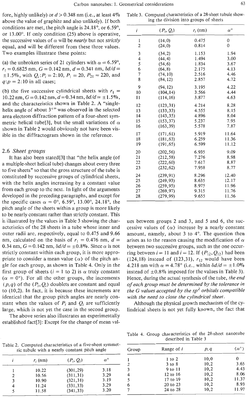
2.6
Sheet
groups
It has also been stated[3] that "the helix angle (of
a
multiple-sheet helical tube) changes about every three
to
five sheets"
so
that the gross structure
of
the tube is
constituted by successive groups of cylindrical sheets,
with the helix angles increasing by a constant value
from each group to the next. In light of the arguments
developed
in
the preceding paragraphs, and except for
the specific cases
a
=
O",
6.59",
13.00",
24.18",
the
pitch angle
of
the sheets within
a
group is more likely
to
be nearly constant rather than strictly constant. This
is illustrated by the values in Table
3
showing the char-
acteristics of the
28
sheets in a tube whose inner and
outer radii are, respectively, equal to
0.475
and
9.66
nm, calculated on the basis of
rl
=
0.476
nm,
d
=
0.34
nm,
G
=
0.142
nm,
6d/d
=
+0.8%.
Since
a
is not
strictly constant within each group, it is more appro-
priate
to
consider a mean value
(a)
of the pitch an-
gle for each group, as shown in Table
4.
Only in the
first group of sheets
(i
=
1
to
2)
is
a
truly constant
(a
=
0").
For all the other groups, the increments
(
p9
q)
of the
(Pi,
Q,)
doublets are constant and equal
to
(10,2).
In fact, it is because these increments are
identical that the group pitch angles are nearly con-
stant when the values
of
Pi
and
Qi
are sufficiently
Iarge, which is not yet the case in the second group.
The above series
also
illustrates an experimentally
established fact[3]: Except for the change
of
mean vd-
Table 2. Computed characteristics of
a
five-sheet symmet-
ric tubule with
a
nearly constant pitch
angle
I
ri
(nm)
(Pi,
Qi)
(Yo
1
10.22
(301,29)
3.18
2 10.56
(31 1,31) 3.29
3
10.90
(321,31) 3.19
4 11.24
(33 1,33) 3.29
5
11.58
(341,33) 3.20
Table
3.
Computed characteristics
of
a
28-sheet tubule show-
ing the division into groups
of
sheets
i
(pi,
Qi)
ri
(nm)
cyo
1
2
3
4
5
6
7
8
9
10
11
12
13
14
1s
16
17
18
19
20
21
22
23
24
25
26
27
28
(14~0)
(24,O)
(34,2)
(44,4)
(54,6)
(64,8)
(74,101
(84,121
(94,12)
(1 14,16)
(123,31)
(133,33)
(143,35)
(1S3,37)
(163,39)
(171,61)
(1 8 1,63)
(191,65)
(202,56)
(212,SS)
(222,60)
(232,62)
(239,9 1)
(249,93)
(259,95)
(269,97)
(279,99)
(104~4)
0.475
0
0.814
0
1.153 1.94
1.494
3
.oo
1.834 3.67
2.175 4.13
2.516 4.46
2.857 4.72
3.195 4.22
3.566 4.44
3.877 4.63
4.214 8.28
4.555 8.15
4.896 8.04
5.237 7.95
5.578 7.87
5.919 11.64
6.259 11.36
6.599 11.12
6.935
9.09
7.276 8.98
7.617 8.87
7.958 8.77
8.296 12.40
8.635 12.17
8.975 11.96
9.315 11.76
9.655 11.56
ues between groups
2
and
3,
and
5
and
6,
the suc-
cessive values of
(a)
increase by a nearly constant
amount, namely, about
3
to
4".
The question then
arises as to the reason causing the modification of
Q!
between two successive groups, such as the one occur-
ring between
i
=
11
and
i
=
12.
If
(P12,
Q12)
had been
(124,18)
instead of
(123,31),
rI2
would have been
4.218
nm with
a
=
4.78"
(Le., within
6d/d
=
+1.0%
instead of
kO.8%
imposed for the values in Table 3).
Hence, during the actual synthesis of the tube,
the end
of
each group must be determined by the tolerance
in
the
G
values accepted by the spz orbitals compatible
with the need to close the cylindrical sheet.
Although the physical growth mechanism
of
the cy-
lindrical sheets is not yet fully known, the fact that
Table 4. Group characteristics
of
the 28-sheet nanotube
described
in
Table
3
Grow Range
of
i
P,
4
(a">
1 1
to
2 10,o
0
3 9
to
11
10,2 4.43
4
12
to
16 10,2 8.06
2
3
to
8 10,2 3.65
5
17 to 19 10,2 11.37
6
20
to 23 10,2 8.93
I
24
to
28 10,2 11.97
64
R.
SETTON
successive sheets have nearly constant helicity suggests
the following mechanism: once the ith (topmost) sheet
is
formed,
C,
species in the gas phase
(n
=
3,1,2.
.
.
,
in order of decreasing abundance[6]) condense onto
the outer surface
of
the tube, probably
at
a distance
slightly larger than 0.34 nm[7], in registry with the un-
derlying substrate and in sp2 hybridization, since this
configuration is the one that best minimizes the energy
of
the system[8]. The ith sheet thus constitutes the
template for the construction
of
the
(i
+
1)th sheet[9],
and the helicity
of
the as-yet-unclosed cylinder during
its formation is the same as that
of
the underlying sub-
strate. This process continues until the
C
atoms
on
ei-
ther side of the cut form the C-C bonds that close
the cylinder. If the geometric characteristics of these
bonds are too different from 120" and
G
=
0.142 nm,
the pitch angle
will
change
to
the immediately higher
or lower value, thus ensuring closure. Once the cylin-
der is closed, and even if closure only involved a single
row of hexagons, the following rows of the cylindri-
cal sheet will necessarily have the same pitch angle, at
least as long as the sheet is growing over an existing
substrate.
2.7
Smallest inner tube diameter
Liu and Cowley[3] have reported the observation
of
innermost cylinders with diameters as small
as
0.7
or 1.3 nm. The first value is only slightly larger than
0.68
nm, the well known diameter
of
the Cs0 mol-
ecule[lO], while the second is in fair agreement with
1.36 nm, the calculated diameter
Cm.
As
shown in
Table
5,
there are 5
(PI,
Q1)
doublets which, with
G
=
0.142 nm, give
rl
=
0.35 nm +3%, and 14
(P1,Q1)
doublets (not all are given in Table 4) for the larger
of
the two values within k5%. It is interesting to find
that there is, in both cases, the possibility of forming
a
non-helical cylindrical sheet with
or
=
Oo,
namely
(P,,Q,)
=
(10,0),
rl
=
0.339 nm, and
(Pl,QI)
=
(20,0),
rl
=
0.678
nm, with the first row of C atoms
corresponding to one of the equatorial cuts of C60 or
of C240; but ignorance of the actual mechanism of
formation of the first cylindrical sheet forbids an ob-
jective choice among the various possibilities.
Table
5.
Some possible characteristics
of
symmetric sheets
with the smallest observed radii
0.339
0.341
0.348
0.352
0.359
0.626
0.644
0.665
0.678
0.679
0
6.59
13.00
30
19.11
30
1.74
30
0
3.30
2.8
Influence
of
the innermost cylinder
If the template effect
of
Endo and Kroto[9] does
indeed exist and the growth
of
the tubule occurs out-
wards,
a
knowledge
of
the Characteristics
of
the inner-
most tube is then of paramount importance in any
attempt at modelizing the structure of
a
symmetric
nanotube[ 111. By reversing eqn (17), possible values
for
P1
and
Q,
can be obtained from
3P;
+
(212
=
(16a2/3)
[(rl/G)2
*
Wr],
(26)
and the inequalities
(8)
and
(9),
provided
rl
has been
determined (say, by HRTEM
-
high resolution trans-
mission electron microscopy), and
G
is
arbitrarily
fixed, say, at
G
=
0.142 nm. Although the task may
become formidable if
r1
and/or
6r/r
are large, the
number of possibilities is strictly limited, especially
since selected area electron diffraction
(SAED)
can
provide narrower limits by giving
a
first approxima-
tion of the pitch angle[3].
3.
CONCLUSION
It is clear that
a
large number
of
parameters influ-
ence the formation of the sheets in
a
tubule and
that
their relative importance
is
still unknown, as is
also
the
cause of the occurrence of the defects responsible for
the eventual polygonization of the sheets. Although
the model presented here highlights the necessity of in-
cluding, as one of the parameters, the uncertainty
6r
or
6d
on the separation of successive cylindrical
sheets,
it
is
impossibIe to predict with absolute certainty the
final characteristics
of
any
of
these sheets, symmetric
or
not,
on
the basis
of
the
characteristics
of
thepre-
vious
one.
Nevertheless, a number of features
of
their
structure, such as the presence or absence
of
helicity,
and the presence of groups of sheets with nearly the
same angle of pitch, can be explained and quantified.
1.
2.
3.
4.
5.
6.
7.
8.
9.
10.
11.
REFERENCES
S.
Iijima,
Nature
354,
56 (1991).
X.
Lin,
X.
K.
Wang,
V.
P.
Dravid,
R.
P.
H. Chang, and
J.
B. Ketterson,
Appl. Phys. Letters
64,
181
(1994).
M.
Liu
and
J.
M.
Cowley,
Carbon
32,
393 (1994).
A. Setton and R. Setton,
Synth. Met.
4,
59 (1981).
T.
W.
Ebbessen and
P.
M. Ajayan,
Nature
358,
220
(1992).
D.
R.
Stull
and
G.
C.
Sinke,
Thermodynamicproperties
of
the elements
(No.
18,
Advances in Chemistry Se-
ries),
pp.
66-69.
American Chemical Society, Washing-
ton
(1956).
L. A. Girifalco and
R.
A.
Lad,
J.
Chem. Phys.
25,693
(1956).
J.-C. Charlier and
J.-P.
Michenaud,
Phys.
Rev.
Lett.
70,
1858
(1993).
M.
Endo and
H.
W.
Kroto,
J.
Phys.
Chem.
96, 6941
(1992).
P.
A. Heiney, J.
E.
Fischer,
A.
R.
McGhie, W.
J.
Romanow,
A.
M.
Denenstein,
J.
P.
McCauley, Jr.,
A.
P.
Smith
111,
and
D.
E.
Cox,
Phys.
Rev.
Lett.
66,291
(199
1).
V.
A. Drits and
C.
Tchoubar,
X-Ray
diffraction by
disordered lamellar structures.
Springer-Verlag, Berlin
(1
990).
SCANNING TUNNELING MICROSCOPY
OF
CARBON
NANOTUBES AND NANOCONES
KLAUS
SATTLER
University of Hawaii, Department of Physics and Astronomy, 2505 Correa Road,
Honolulu, HI 96822, U.S.A.
(Received
18
July
1994;
accepted
10
February
1995)
Abstract-Tubular and conical carbon shell structures can be synthesized in the vapor phase. Very hot car-
bon vapor, after being deposited onto highly oriented pyrolytic graphite (HOPG), forms a variety
of
nano-
structures, in particular single-shell tubes, multishell
tubes,
bundles
of
tubes, and cones. The structures
were analyzed by scanning tunneling microscopy
(STM)
in UHV. Atomic resolution images show directly
the surface atomic structures
of
the tubes and their helicities.
A
growth pathway
is
proposed for fuiler-
enes, tubes, and cones.
Hey
Words-Carbon nanotubes, fullerenes,
STM,
fibers, nanostructures, vapor growth.
1.
INTRODUCTION
Hollow carbon nanostructures are exciting new sys-
tems for research and for the design of potential nano-
electronic devices. Their atomic structures are closely
related to their oute: shapes and are described by hex-
agonal/penitagonal network configurations. The sur-
faces of such structures are atomically smooth and
perfect. The most prominent of these objects are ful-
lerenes and nanotubes[l]. Other such novel structures
are carbon onions[2] and nanocones[3].
Various techniques have been used to image nano-
tubes: scanning electron microscopy (SEM)[
11,
scan-
ning tunneling microscopy (STM)[4-71, and atomic
force microscopy (AFM)[S]. Scanning probe micro-
scopes are proximity probes. They can provide three-
dimensional topographic images and, in addition, can
give the atomic structure of the surface net. They can
also be used to measure the electronic (STM) and elas-
tic (AFMJ properties of small structures. STM
is
re-
stricted to electrically conducting objects, but AFM
does not have this constraint.
STM and AFM images give directly the three-
dimensional morphology of tubes and are consistent
with the structures inferred from SEM.
In
addition,
atomically resolved STM images make direct helicity
determinations possible[4]. They give information
about the nature of stacking of concentric carbon lay-
ers within the nanotubes via modifications of their sur-
face density of states. STM is sensitive
to
such small
lateral local density of states variations. Contours
taken from the ends of the tubes show that some
of
them are open and others are closed. Many images in-
dicate that the closed tubes have hemispherical caps.
Such terminations can be modeled by fullerene hemi-
spheres with
5/6
networks.
IC
is
not
easy to determine detailed properties
of
the
tube terminations using STM or AFM. These micro-
scopes cannot image undercut surfaces and the tip
shape
is
convoluted with the cap shape of the nano-
tube. However, the tips may have very sharp edges
yielding quite realistic three-dimensional images from
tube terminations.
Also,
besides a difference in rnor-
phology, open and closed ends show a difference in
electronic structure. Open ends appear with ‘highlighted’
edges in STM images, which
is
due
to
an enhanced
dangling bond electron state density. Closed ends
do
not have such highlighted edges.
The growth pathway of various fullerene- and
graphene-type nano-objects may be related. They are
synthesized in the vapor phase and often appear simul-
taneously on the same sample.
A
common growth
mechanism with similar nucleation seeds may, there-
fore, lead to these different structures.
2.
EXPERIMENTAL
Graphite was used as substrate for the deposition
of carbon vapor. Prior to the tube and cone studies,
this substrate was studied by
us
carefully by STM be-
cause it may exhibit anomalous behavior with unusual
periodic surface structures[9,10].
In
particular, the
cluster-substrate interaction was investigated[l
11.
At
low submonolayer coverages, small clusters and
is-
lands are observed. These tend
to
have linear struc-
tures[l2]. Much higher coverages are required for the
synthesis of nanotubes and nanocones.
In
addition, the
carbon vapor has to be very hot, typically >3O0O0C.
We note that the production of nanotubes by arc dis-
charge occurs also at an intense heat (of the plasma
in the arc) of >30OO0C.
The graphite (grade-A HOPG) was freshly cleaved
in
UHV
and carefully examined by STM before the
deposition. The HOPC surface was determined
to
be
atomically flat and defect-free over micrometer dimen-
sions. Any defect or adatom would have easily been
detected. The graphite was cooled
to
-30°C during
evaporation. The carbon vapor was produced by re-
sistively heating a 99.99% purity carbon foil
(0.5
mrri
thick) in
UHV
(base pressure
2
x
lo-’
Torr). The de-
position rate of
0.5
A/s
was controlled by a quartz
crystal film thickness monitor. After deposition, the
65
66
K.
SATTLER
samples were transferred to a STM operated at
2
x
lo-''
Torr, without breaking vacuum. Our evapora-
tion and condensation process leads to the formation
of various nanostructures, with
70%
nanotubes on the
average, of the overall products. In some areas, which
may be
as
large as one square micron, we find
100%
nanotubes. The yield for single-wall tubes varied from
experiment to experiment from
a
few percent to
80-
90%.
Bundles of multiwall tubes were found in some
areas, but were usually less abundant than isolated
tubes. Individual nanocones were observed together
with tubes, but were quite seldom. The microscope was
operated in the constant current and in the constant
height mode. Atomic resolution images were recorded
in the constant current mode, in which the tip-to-
sample distance is kept constant by means
of
an elec-
tronic feedback control. Bias voltages of
100
to
800
mV (both positive and negative) and tunneling cur-
rents of
0.5
to 3.0 nA were applied. A mechanically
shaped Pt/lr tip was used.
We did not observe any voltage dependent varia-
tion of the tube images. Also, the measured heights
of the tubes were comparable with their diameters.
Both of these observations indicate that the tubes have
rather metallic than semiconducting properties.
The tubes were stable over long periods of time.
After several months of being stored in UHV we still
observed the same features as shortly after their prep-
aration. Some of the samples were transferred to an
STM
operated in air. Again, we observed similar
structures as seen in UHV. This shows the high stability
of the tubes. It appears that the vapor-phase growth
technique produces defect-free tubes, with dangling
bonds at the tube edges often being saturated by cap
terminations.
3.
SINGLESHELL TUBES
Single-shell tubes are formed from a single layer
of
graphite. The surface
of
the cylinders has
a
honeycomb-
lattice pattern, just as in
a
two-dimensional graphite
plane. From
a
theoretical point of view they are inter-
esting as the embodiment
of
a
one-dimensional
(1-D)
periodic structure along the tube axis. In the circum-
ferential direction, periodic boundary conditions ap-
ply
to
the enlarged unit cell. In addition to the chiral
structures, there exist two nonchiral configurations,
zigzag and armchair
[
131.
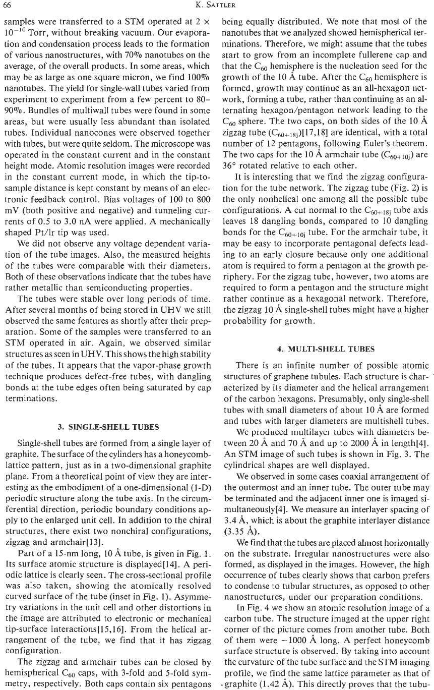
Part of
a
15-nm long,
10
A
tube, is given in Fig.
1.
Its surface atomic structure is displayedIl41. A peri-
odic lattice is clearly seen. The cross-sectional profile
was also taken, showing the atomically resolved
curved surface of the tube (inset in Fig.
1).
Asymme-
try variations in the unit cell and other distortions in
the image are attributed to electronic or mechanical
tip-surface interactions[l5,16]. From the helical ar-
rangement of the tube, we find that it has zigzag
configuration.
The zigzag and armchair tubes can be closed by
hemispherical
C6'
caps, with 3-fold and 5-fold sym-
metry, respectively. Both caps contain six pentagons
being equally distributed. We note that most
of
the
nanotubes that we analyzed showed hemispherical ter-
minations. Therefore, we might assume that the tubes
start
to
grow from an incomplete fullerene cap and
that the
C,,
hemisphere is the nucleation seed
for
the
growth of the 10
A
tube. After the
C6'
hemisphere is
formed, growth may continue as an all-hexagon net-
work, forming
a
tube, rather than continuing
as
an al-
ternating hexagodpentagon network leading to the
C6,
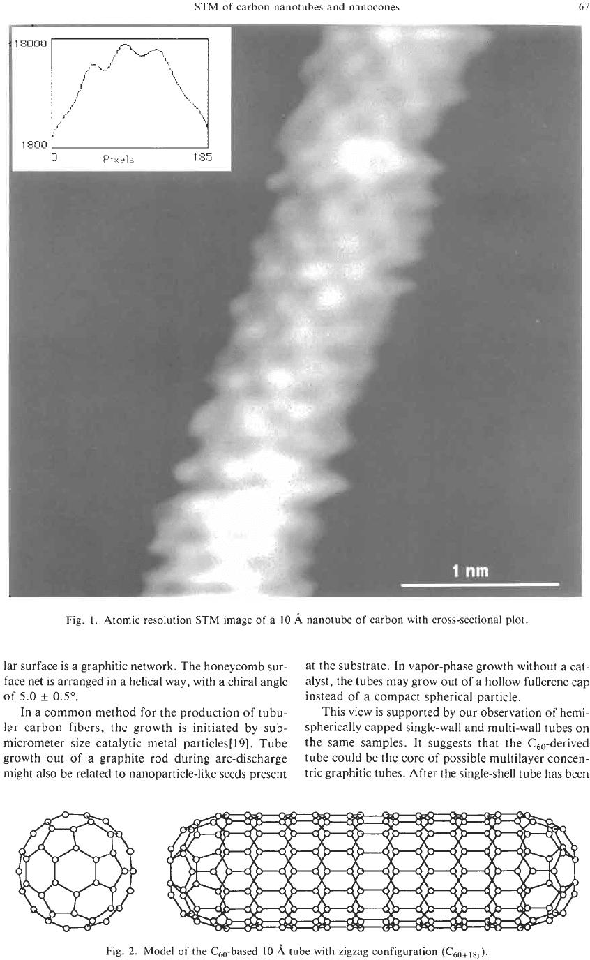
sphere. The two caps, on both sides
of
the 10
A
zigzag tube (C60+18j)[17,1S] are identical, with
a
total
number
of
12 pentagons, following Euler's theorem.
The two caps for the
10
A
armchair tube
(C60+10j)
are
36"
rotated relative to each other.
It is interesting that we find the zigzag configura-
tion for the tube network. The zigzag tube (Fig.
2)
is
the only nonhelical one among all the possible tube
configurations.
A
cut normal to the
C60+18j
tube axis
leaves
18
dangling bonds, compared to
10
dangling
bonds for the
C60+10j
tube. For the armchair tube, it
may be easy to incorporate pentagonal defects lead-
ing to an early closure because only one additional
atom is required to form a pentagon at the growth pe-
riphery. For the zigzag tube, however, two atoms are
required to form a pentagon and the structure might
rather continue as a hexagonal network. Therefore,
the zigzag
10
A
single-shell tubes might have a higher
probability for growth.
4.
MULTI-SHELL TUBES
There is an infinite number of possible atomic
structures of graphene tubules. Each structure is char-
acterized by its diameter and the helical arrangement
of the carbon hexagons. Presumably, only single-shell
tubes with small diameters
of
about
10
A
are formed
and tubes with larger diameters are multishell tubes.
We produced multilayer tubes with diameters be-
tween
20
A
and
70
A
and up
to
2000
A
in length[4].
An
STM
image
of
such tubes is shown in Fig. 3. The
cylindrical shapes are well displayed.
We observed in some cases coaxial arrangement of
the outermost and
an
inner tube. The outer tube may
be terminated and the adjacent inner one is imaged si-
multaneously[4]. We measure an interlayer spacing of
3.4
A,
which is about the graphite interlayer distance
We find that the tubes are placed almost horizontally
on the substrate. Irregular nanostructures were also
formed, as displayed in the images. However, the high
occurrence
of
tubes clearly shows that carbon prefers
to
condense
to
tubular structures, as opposed
to
other
nanostructures, under our preparation conditions.
In Fig. 4 we show an atomic resolution image of
a
carbon tube. The structure imaged at the upper right
corner of the picture comes from another tube. Both
of
them were -1000
A
long.
A
perfect honeycomb
surface structure is observed. By taking into account
the curvature
of
the tube surface and the
STM
imaging
profile, we find the same lattice parameter as that of
.graphite (1.42
A).
This directly proves that the tubu-
(3.35
A).
STM
of
carbon nanotubes and nanocones
61
Fig.
1.
Atomic resolution STM image
of
a
10
A
nanotube
of
carbon with cross-sectional plot.
lar surface is a graphitic network. The honeycomb sur-
face net
is
arranged in a helical way, with a chiral angle
of
5.0
f
0.5".
In a common method for the production of tubu-
lar carbon fibers, the growth is initiated by sub-
micrometer size catalytic metal particles[
191.
Tube
growth out
of
a
graphite rod during arc-discharge
might also be related to nanoparticle-like seeds present
at the substrate. In vapor-phase growth without a cat-
alyst, the tubes may grow out
of
a hollow fullerene cap
instead
of
a compact spherical particle.
This view is supported by our observation of hemi-
spherically capped single-wall and multi-wall tubes on
the same samples. It suggests that the C,,-derived
tube could be the core
of
possible multilayer concen-
tric graphitic tubes. After the single-shell tube has been
Fig. 2. Model of the Cm-based
10
A
tube with zigzag configuration (C,,+,,j).