Endo M., Iijima S., Dresselhaus M.S. (eds.) Carbon nanotubes
Подождите немного. Документ загружается.

28
M.
S.
DRESSELHAUS
ef
al.
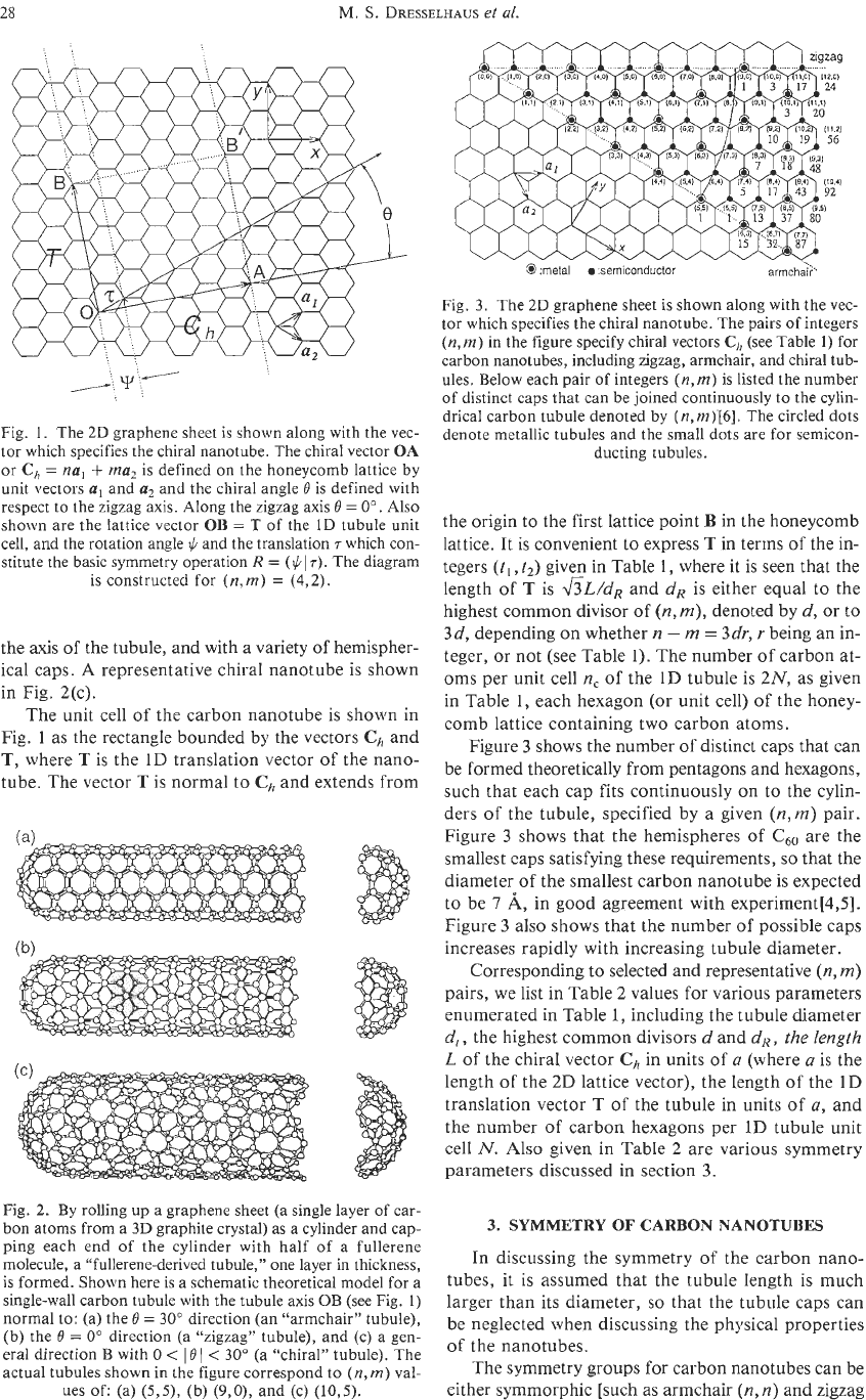
Fig.
1.
The
2D
graphene sheet is shown along with the vec-
tor which specifies the chiral nanotube. The chiral vector
OA
or
C,
=
nu,
+
ma,
is defined
on
the honeycomb lattice by
unit vectors
a,
and u2 and the chiral angle
6
is defined with
respect to the zigzag axis.
Along
the zigzag axis
6
=
0”.
Also
shown are the lattice vector
OB
=
T
of the
1D
tubule unit
cell, and the rotation angle
$
and the translation
T
which con-
stitute the basic symmetry operation
R
=
($1
7).
The diagram
is constructed for
(n,rn)
=
(4,2).
the
axis
of the tubule, and with
a
variety of hemispher-
ical caps.
A
representative chiral nanotube is shown
in Fig. 2(c).
The unit cell of the carbon nanotube is shown in
Fig.
1
as the rectangle bounded by the vectors
Ch
and
T,
where
T
is the ID translation vector
of
the nano-
tube. The vector
T
is normal to
Ch
and extends from
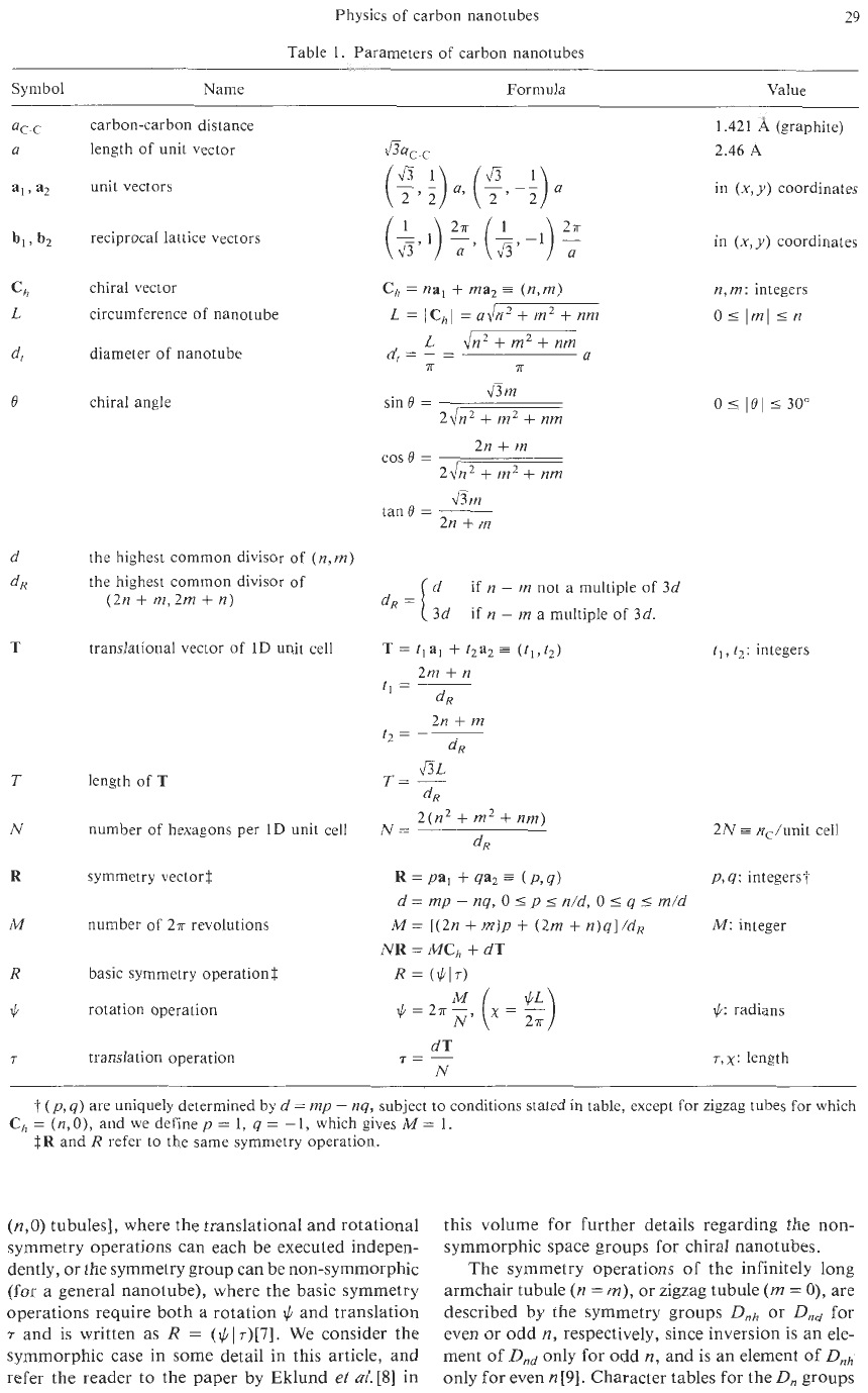
Fig.
2.
By rolling up
a
graphene sheet (a single layer of car-
bon
atoms from a
3D
graphite crystal) as a cylinder and cap-
ping each end
of
the cylinder with half
of
a fullerene
molecule, a “fullerene-derived tubule,” one layer in thickness,
is formed. Shown here is a schematic theoretical model
for
a
single-wall carbon tubule with the tubule axis
OB
(see Fig.
1)
normal to: (a) the
0
=
30”
direction (an “armchair” tubule),
(b) the
0
=
0”
direction (a “zigzag” tubule), and (c) a gen-
eral direction
B
with
0
<
16
I
<
30”
(a “chiral” tubule). The
actual tubules shown in the figure correspond to
(n,m) val-
ues
of: (a)
(5,5),
(b)
(9,0),
and (c)
(10,5).
@
:metal
:semiconductor
armcha?’
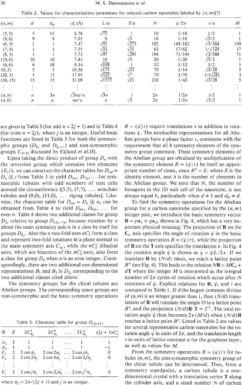
Fig,
3.
The
2D
graphene sheet is shown along with the vec-
tor which specifies the chiral nanotube. The pairs
of
integers
(n,rn)
in the
figure
specify chiral vectors
Ch
(see Table
1)
for
carbon nanotubes, including Zigzag, armchair, and chiral tub-
ules. Below each pair
of
integers
(n,rn)
is listed the number
of
distinct caps that can be joined continuously
to
the cylin-
drical carbon tubule denoted
by
(n,m)[6]. The circled dots
denote metallic tubules and the small dots are
for
semicon-
ducting tubules.
the origin to the first lattice point
B
in the honeycomb
lattice. It is convenient to express
T
in terms of the in-
tegers
(t,
,
f2)
given
in
Table 1, where it is seen that the
length of
T
is
&L/dR
and
dR
is either equal to the
highest common divisor of
(n,rn),
denoted by
d,
or
to
3d,
depending on whether
n
-
rn
=
3dr,
r
being
an
in-
teger, or not (see Table
1).
The number
of
carbon at-
oms per unit cell
n,
of the
1D
tubule is
2N,
as
given
in Table
1,
each hexagon (or unit cell) of the honey-
comb lattice containing two carbon atoms.
Figure
3
shows the number of distinct caps that can
be formed theoretically from pentagons and hexagons,
such that each cap fits continuously
on
to
the cylin-
ders
of
the tubule, specified by a given
(n,m)
pair.
Figure
3
shows that the hemispheres of C,, are the
smallest caps satisfying these requirements,
so
that the
diameter of the smallest carbon nanotube
is
expected
to be
7 A,
in good agreement with experiment[4,5].
Figure
3
also shows that the number of possible caps
increases rapidly with increasing tubule diameter.
Corresponding to selected and representative
(n,
rn)
pairs, we list in Table 2 values for various parameters
enumerated in Table 1, including the tubule diameter
d,,
the highest common divisors
d
and
dR,
the
length
L
of
the chiral vector
Ch
in units of
a
(where a
is
the
length
of
the 2D lattice vector), the length of the 1D
translation vector
T
of the tubule in units
of
a,
and
the number of carbon hexagons per 1D tubule unit
cell
N.
Also given in Table 2 are various symmetry
parameters discussed in section
3.
3.
SYMMETRY
OF
CARBON NANOTUBFS
In
discussing the symmetry
of
the carbon nano-
tubes,
it
is assumed that the tubule length is much
larger than its diameter,
so
that the tubule caps can
be neglected when discussing the physical properties
of the nanotubes.
The symmetry groups for carbon nanotubes can be
either symmorphic [such as armchair
(n,n)
and zigzag
Physics
of
carbon nanotubes
29
Table 1. Parameters
of
carbon nanotubes
Symbol Name Formula
Value
___
carbon-carbon distance
length
of
unit vector
unit vectors
reciprocal lattice vectors
chiral vector
circumference
of
nanotube
diameter
of
nanotube
chiral angle
the highest common divisor
of
(n,
m)
the highest common divisor
of
(2n
+
m,2m
+
n)
translational vector
of
1D unit cell
length
of
T
number of hexagons per 1D unit cell
symmetry vector$
number of
2n
revolutions
basic symmetry operation$
rotation operation
translation operation
Ch
=
na,
+
ma2
=
(n,m)
L=
/C,I
=uJn~+m2+nm
L
Jn’+m’+nm
d,=
-
z
li
7r
7r
2n
+
m
2Jn2
+
m2
+
nm
cos
0
=
am
tan
0
=
-
2n
+
m
d
3d
if
n
-
m
not
a multiple
of
3d
if
n
-
m
a multiple of
3d.
dR=(
T
=
t,a,
+
f2a2
=
(11,12)
2m
+
n
t,
=
~
2n
+
m
1,
=
-~
aL
dR
2(n2
+
in2
+
nm)
dR
dR
dR
T=
-
N=
1.421
*4
(graphite)
2.46
A
in
(x,y)
coordinates
in
(x,y)
coordinates
n,
m:
integers
Oslmlsn
t,
,
t,:
integers
2N
=
n,/unit cell
R
=pa,
+
qa2
=
(nq)
d
=
mp
-
nq,
0
5
p
s
n/d,
0
5
q
5
m/d
M=
[(2n
+
m)p
+
(2m
+
n)q]/d,
R
=
($17)
p,
q:
integers?
M:
integer
NR
=
MCh
+
dT
dT
N
71-
6:
radians
T,X:
length
t
(p,
q)
are uniquely determined by
d
=
mp
-
nq,
subject to conditions stated in table, except for zigzag tubes for which
$R
and
R
refer to the same symmetry operation.
C,
=
(n,O),
and we definep
=
1,
q
=
-1,
which gives
M=
1.
(n,O)
tubules], where the translational and rotational
symmetry operations can each be executed indepen-
dently, or the symmetry group
can
be non-symmorphic
(for
a
general nanotube), where the basic symmetry
operations require both
a
rotation
$
and translation
r
and is written as
R
=
($1
r)[7].
We consider the
symmorphic case in some detail
in
this article, and
refer the reader to the paper by Eklund
et
al.[8]
in
this volume for further details regarding the
non-
symmorphic space groups for chiral nanotubes.
The symmetry operations of the infinitely long
armchair tubule
(n
=
m),
or zigzag tubule
(rn
=
0),
are
described by the symmetry groups
Dnh
or
Dnd
for
even or odd
n,
respectively, since inversion
is
an ele-
ment of
Dnd
only for odd
n,
and is an element
of
Dnh
only for even
n
[9].
Character tables for the
D,
groups
30
M.
S.
DRESSELHAUS
et
ai.
Table 2. Values
for
characterization parameters
for
selected carbon nanotubes labeled
by
(n,rn)[7]
(n,
m)
d
dR
d,
(A)
L/a
T/a
N
$/2n
7/a
A4
5
15
9 9
1 1
1
3
1 1
10 10
6
18
5
5
5
15
15 15
n
3n
n n
6.78
7.05
7.47
1.55
7.72
7.83
8.14
10.36
17.95
31.09
&a/n
na/T
475
1 10
9
fi
18
m
m
182
J93
m
62
m
m
194
10
43
20
m
1 12
m
621
210
6175
m
70
6525
d7
70
fin
1
2n
n
A
2n
1/10
1/18
149/ 182
11/62
71/194
1 /20
1/12
1/14
3/70
1 /42
1/2n
1/2n
1
/2
A/2
&ma
1/,1124
631388
v3/2
63/28
l/(JZs)
m
1
/2
1 /2
fi/2
1
1
149
17
11
1
1
5
3
5
1
1
are given in Table
3
(for odd
n
=
2j
+
1)
and in Table
4
(for even
n
=
2j),
wherej is an integer. Useful basis
functions are listed in Table
5
for both the symmor-
phic groups
(D2j
and
DzJ+,)
and non-symmorphic
groups
C,,,
discussed by Eklund
ef
al.
[8].
Upon taking the direct product of group
D,
with
the inversion group which contains two elements
(E,
i),
we can construct the character tables for
Dnd
=
D,
@
i
from Table
3
to yield
D,,,
D,,,
.
.
.for sym-
morphic tubules with odd numbers
of
unit cells
around the circumference
[(5,5),
(7,7),
.
.
.
armchair
tubules and
(9,0),
(ll,O),
.
. .
zigzag tubules]. Like-
wise, the character table for
Dnh
=
0,
@
ah
can be
obtained from Table
4
to yield
D6h, Dsh,
. .
.
for
even
n.
Table
4
shows two additional classes for group
D,
relative to group
D(zJ+l),
because rotation by
.rr
about the main symmetry axis is in a class by itself for
groups
D2j.
Also the
n
two-fold axes
nC;
form a class
and represent two-fold rotations in a plane normal to
the main symmetry axis
C,,
,
while the
nCi
dihedral
axes, which are bisectors of the
nC;
axes, also form
a class for group
D,,
when
n
is an even integer. Corre-
spondingly, there are two additional one-dimensional
representations
B,
and
B2
in
DZi
corresponding to the
two additional classes cited above.
The symmetry groups for the chiral tubules are
Abelian groups. The corresponding space groups are
non-symmorphic and the basic symmetry operations
Table 3. Character table for
group
D(u+l,
CR
E
2C;j 2C:;
...
2Ci, (2j+ 1)C;
AI
1
1
1
...
1
1
'42
1 1 1
...
1 -1
E,
2 2~0~6~
2~0~26~
.
.
.
2co~j6~
0
E,
2
2c0s2+~
2~0~44~
.
.
.
2c0s2j+~
0
..
E,
2 2c0sjbj 2cos2j6,
. .
. 2cos
j2c+5j
0
where
=
27/(2j
+
1) and
j
is
an integer
R
=
($1
T)
require translations
T
in addition
to
rota-
tions
$.
The irreducible representations for all Abe-
lian groups have a phase factor
E,
consistent with the
requirement that all
h
symmetry elements of the sym-
metry group commute. These symmetry elements of
the Abelian group are obtained by multiplication of
the symmetry element
R
=
($
IT)
by itself an appro-
priate number of times, since
Rh
=
E,
where
E
is the
identity element, and
h
is the number of elements in
the Abelian group. We note that
N,
the number
of
hexagons in the
1D
unit cell
of
the nanotube, is
not
always equal
h,
particularly when
d
#
1
and
dR
#
d.
To
find the symmetry operations for the Abelian
group for
a
carbon nanotube specified by the
(n,
rn)
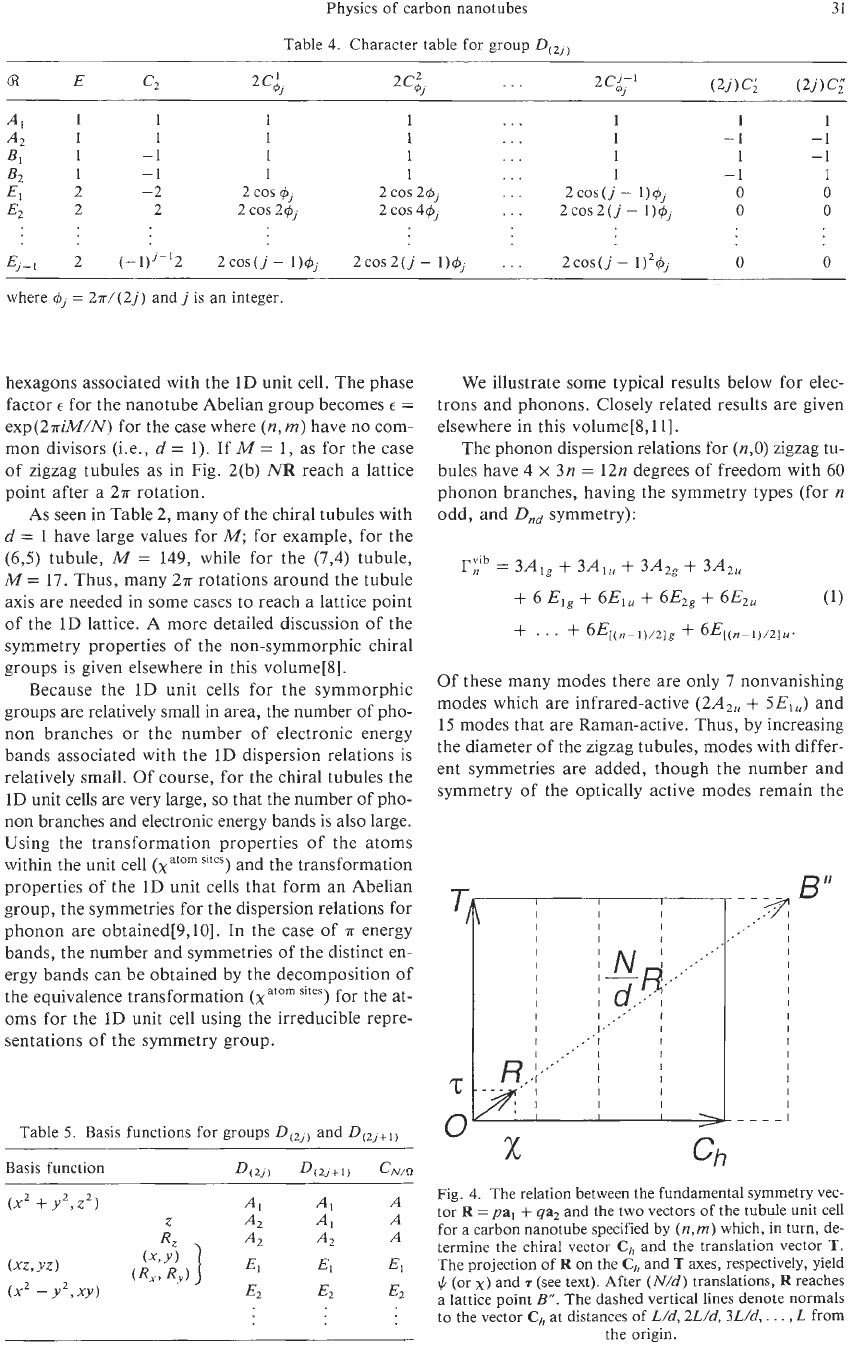
integer pair, we introduce the basic symmetry vector
R
=pa,
+
qa,,.
shown in Fig.
4,
which has a very im-
portant physical meaning. The projection
of
R
on
the
Ch
axis specifies the angle of rotation
$
in the basic
symmetry operation
R
=
(3
IT),
while the projection
of
R
on
the
T
axis specifies the translation
7.
In Fig.
4
the rotation angle
$
is
shown as
x
=
$L/2n.
If we
translate
R
by
(N/d)
times, we reach
a
lattice point
B"
(see Fig.
4).
This
leads to the relationm
=MCh
+
dT
where the integer
M
is interpreted
as
the integral
number
of
27r
cycles of rotation which occur after
N
rotations of
$.
Explicit relations for
R,
$,
and
T
are
contained in Table
1.
If
d
the largest common divisor
of
(n,rn)
is an integer greater than
I,
than
(N/d)
trans-
lations
of
R
will translate the origin
0
to a lattice point
B",
and the projection
(N/d)R.T
=
T2.
The total ro-
tation angle $then becomes
2.rr(Mld)
when
(N/d)R
reaches
a
lattice point
B".
Listed in Table
2
are values
for several representative carbon nanotubes for the ro-
tation angle
$
in units of
27r,
and the translation length
T
in units
of
lattice constant
a
for the graphene layer,
as well as values for
M.
From the symmetry operations
R
=
(4
IT)
for tu-
bules
(n,
rn),
the non-symmorphic symmetry group of
the chiral tubule can be determined. Thus, from a
symmetry standpoint, a carbon tubule is a one-
dimensional crystal with a translation vector
T
along
the cylinder axis, and
a
small number
N
of carbon
Physics of carbon nanotubes
31
AI
1
1
1
1
...
1
1
1
A2
1
1
1
1
...
1
-1
-1
Bl
1
-1
1
1
...
1
I
-1
B2
1
-1
1
1
...
1
-1
1
El
2 -2 2 cos
Gj
2
cos 24j
.
.
.
2cos(j
-
l)+j
0
0
E2
2 2 2 cos 2Gj
2 cos
4+j
.
.
.
2COS2(j
-
l)+j
0
0
Ej-!
2 (-1)j-’2 2cos(j-
l)bj
2cos2(j-
1)4
...
2cos(j-
l)2+j
0
0
where
$,
=
27r/(2j) and
j
is an integer.
hexagons associated with the 1D unit cell. The phase
factor
E
for the nanotube Abelian group becomes
E
=
exp(27riM/N for the case where
(n,m)
have
no
com-
mon divisors (i-e.,
d
=
1). If
M
=
1, as for the case
of zigzag tubules as in Fig. 2(b)
NR
reach a lattice
point after a 2n rotation.
As seen in Table 2, many of the chiral tubules with
d
=
1 have large values for
M;
for example, for the
(6J) tubule,
M
=
149, while for the (7,4) tubule,
M
=
17. Thus, many 2~ rotations around the tubule
axis are needed in some cases to reach a lattice point
of the
1D
lattice. A more detailed discussion
of
the
symmetry properties of the non-symmorphic chiral
groups is given elsewhere in this volume[8].
Because the 1D unit cells for the symmorphic
groups are relatively small in area, the number of pho-
non
branches or the number of electronic energy
bands associated with the 1D dispersion relations is
relatively small. Of course, for the chiral tubules the
1D unit cells are very large,
so
that the number of pho-
non
branches and electronic energy bands is aIso large.
Using the transformation properties of the atoms
within the unit cell
(xatom
’IfeS
)
and the transformation
properties
of
the
1D
unit cells that form an Abelian
group, the symmetries for the dispersion relations for
phonon are obtained[9,10]. In the case of
n
energy
bands, the number and symmetries of the distinct en-
ergy bands can be obtained by the decomposition of
the equivalence transformation
(xatom
sites
)
for the at-
oms for the
ID
unit cell using the irreducible repre-
sentations of the symmetry group.
Table
5.
Basis functions for groups
D(2,)
and
Do,+,,
We illustrate some typical results below for elec-
trons and phonons. Closely related results are given
elsewhere
in
this volume[8,1
I].
The phonon dispersion relations for
(n,O)
zigzag tu-
bules have
4
x
3n
=
12n degrees of freedom with 60
phonon branches, having the symmetry types (for
n
odd, and
Dnd
symmetry):
Of
these many modes there are only
7
nonvanishing
modes which are infrared-active (2A2,
+
5E1,) and
15 modes that are Raman-active. Thus, by increasing
the diameter of the zigzag tubules, modes with differ-
ent symmetries are added, though the number and
symmetry of the optically active modes remain the
-x
ch
Fig.
4.
The relation between the fundamental symmetry vec-
tor
R
=pa,
+
qaz
and the two vectors of the tubule unit cell
for a carbon nanotube specified by
(n,m)
which, in turn, de-
termine the chiral vector
C,
and the translation vector
T.
The projection of
R
on
the
C,,
and
T
axes, respectively, yield
(or
x)
and
T
(see text). After
(N/d)
translations,
R
reaches
a
lattice point
B”.
The dashed vertical lines denote normals
to
the vector
C,
at
distances of
L/d,
X/d,
3L/d,.
.
.
,
L
from
the origin.
32
M.
S.
DRESSZLHAUS
et
a/.
same. This is
a
symmetry-imposed result that is gen-
erally valid for all carbon nanotubes.
Regarding the electronic structure, the number of
energy bands for
(n,O)
zigzag carbon nanotubes is
2n,
the number of carbon atoms per unit cell, with
symmetries
A symmetry-imposed band degeneracy occurs for the
Ef+3)/21g
and
EE(~-~,~~~
bands at the Fermi level,
when
n
=
3r, r being an integer, thereby giving rise
to zero gap tubules with metallic conduction. On the
other hand, when
n
#
3r, a bandgap and semicon-
ducting behavior results. Independent of whether the
tubules are conducting or semiconducting, each of
the
[4
+
2(n
-1)J
energy bands is expected to show a
(E
-
Eo)-1’2
type singularity in the density of states
at
its band extremum energy
Eo
[
101.
The most promising present technique for carrying
out sensitive measurements
of
the electronic proper-
ties of individual tubules is scanning tunneling spec-
troscopy (STS) becaise
of
the ability of the tunneling
tip to probe most sensitively the electronic density
of
states
of
either a single-wall nanotube[l2], or the out-
ermost cylinder
of
a multi-wall tubule or, more gen-
erally, a bundle
of
tubules. With this technique, it is
further possible to carry
out
both STS and scanning
tunneling microscopy (STM) measurements at the
same location on the same tubule and, therefore, to
measure the tubule diameter concurrently with the STS
spectrum.
Although still preliminary, the study that provides
the most detailed test of the theory for the electronic
properties
of
the
ID
carbon nanotubes, thus far, is the
combined STMISTS study by Olk and Heremans[ 131.
In this STM/STS study, more than nine individual
.multilayer tubules with diameters ranging from 1.7 to
9.5
nm
were examined. The
I-
Vplots provide evidence
for both metallic and semiconducting tubules[ 13,141.
Plots of dl/dVindicate maxima in the
1D
density of
states, suggestive of predicted singularities in the 1D
density of states for carbon nanotubes. This STM/
STS study further shows that the energy gap for the
semiconducting tubules is proportional to the inverse
tubule diameter
lid,,
and is independent
of
the tubule
chirality.
4.
MULTI-WALL
NANOTUBES
AND
ARRAYS
Much of the experimental observations
on
carbon
nanotubes thus far have been made
on
multi-wall tu-
bules[15-19]. This has inspired a number of theoretical
calculations to extend the theoretical results initially
obtained for single-wall nanotubes to observations in
multilayer tubules. These calculations for multi-wall
tubules have been informative for the interpretation
of
experiments, and influential for suggesting new re-
search directions. The multi-wall calculations have
been predominantly done for double-wall tubules, al-
though some calculations have been done for a four-
walled tubule[16-18] and also for nanotube arrays
[
16,171.
The first calculation for a double-wall carbon
nanotube[l5] was done using the tight binding tech-
nique, which sensitively includes all symmetry con-
straints in
a
simplified Hamiltonian. The specific
geometrical arrangement that was considered is the
most commensurate case possible for a double-layer
nanotube, for which the ratio
of
the chiral vectors for
the two layers is 1
:2,
and in the direction of transla-
tional vectors, the ratio
of
the lengths is 1
:
1.
Because
the C60-derived tubule has a radius of 3.4
A,
which is
close to the interlayer distance for turbostratic graph-
ite, this geometry corresponds to the minimum diam-
eter for a double-layer tubule. This geometry has
many similarities to the AB stacking of graphite. In
the double-layer tubule with the diameter ratio 1:2, the
interlayer interaction
y1
involves only half the num-
ber
of
carbon atoms as in graphite, because of the
smaller number
of
atoms
on
the inner tubule. Even
though the geometry was chosen
to
give rise to the
most commensurate interlayer stacking, the energy
dispersion relations are only weakly perturbed by the
interlayer interaction.
More specifically, the calculated energy band struc-
ture showed that two coaxial zigzag nanotubes that
would each be metallic as single-wall nanotubes yield
a metallic double-wall nanotube when a weak inter-
layer coupling between the concentric nanotubes is
introduced. Similarly, two coaxial semiconducting tu-
bules remain semiconducting when the weak interlayer
coupling is introduced[l5]. More interesting is the case
of coaxial metal-semiconductor and semiconductor-
metal nanotubes, which also retain their individual
metallic and semiconducting identities when the weak
interlayer interaction
is
turned on. On the basis of this
result, we conclude that it might be possible to prepare
metal-insulator device structures in the coaxial geom-
etry without introducing any doping impurities[20], as
has already been suggested in the literature[10,20,21].
A
second calculation was done for a two-layer tu-
bule using density functional theory in the local den-
sity approximation to establish the optimum interlayer
distance between an inner
(53)
armchair tubule and
an
outer armchair (10,lO) tubule. The result
of
this
calculation yielded
a
3.39
A
interlayer separation
[16,17], with an energy stabilization
of
48
meV/car-
bon atom. The fact that the interlayer separation is
about halfway between the graphite value of 3.35
A
and the 3.44
A
separation expected for turbostratic
graphite may be explained by interlayer correlation be-
tween the carbon atom sites both along the tubule axis
direction and circumferentially.
A
similar calculation
for double-layered hyper-fullerenes has also been car-
ried out, yielding an interlayer spacing of 3.524
A
for
C60@C240 with an energy stabilization
of
14 meV/C
atom for this case[22]. In the case of the double-
layered hyper-fullerene, there is
a
greatly reduced pos-
Physics
of
carbon nanotubes
33
sibility for interlayer correlations, even if
C60
and
CZm
take the same
I),
axes. Further, in the case
of
C240,
the molecule deviates from
a
spherical shape to
an icosahedron shape. Because of the curvature, it is
expected that the spherically averaged interlayer spac-
ing between the double-layered hyper-fullerenes is
greater than that for turbostratic graphite.
In addition, for two coaxial armchair tubules, es-
timates for the translational and rotational energy
barriers
(of
0.23 meV/atom and
0.52
meV/atom, re-
spectively) were obtained, suggesting significant trans-
lational and rotational interlayer mobility
of ideal
tubules at room temperature[l6,17]. Of course, con-
straints associated with the cap structure and with de-
fects on the tubules would be expected
to
restrict these
motions. The detailed band calculations for various
interplanar geometries for the two coaxial armchair tu-
bules basically confirm the tight binding results men-
tioned above[ 16,171.
Further calculations are needed to determine whether
or
not a Peierls distortion might remove the coaxial
nesting of carbon nanotubes. Generally 1D metallic
bands are unstable against weak perturbations which
open an energy gap at
EF
and consequently lower the
total energy, which is known as the Peierls instabil-
ity[23]. In the case of carbon nanotubes, both in-plane
and out-of-plane lattice distortions may couple with
the electrons at the Fermi energy. Mintmire and White
have discussed the case of in-plane distortion and have
concluded that carbon nanotubes are stable against a
Peierls distortion in-plane at room temperature[24],
though the in-plane distortion, like a KekulC pattern,
will be at least
3
times as large a
unit
cell as that of
graphite. The corresponding chiral vectors satisfy the
condition for metallic conduction
(n
-
m
=
3r,r:in-
teger). However, if we consider the direction of the
translational vector
T,
a
symmetry-lowering distortion
is not always possible, consistent with the boundary
conditions for the general tubules[25]. On the other
hand, out-of-plane vibrations do not change the size
of the unit cell, but result in
a
different site energy for
carbon atoms
on
A
and
B
sites for carbon nanotube
structures[26]. This situation is applicable, too,
if
the
dimerization is of the “quinone” or chain-like type,
where out-of-plane distortions lead to a perturbation
approaching the limit of
2D
graphite. Further, Hari-
gaya and Fujita[27,28] showed that an in-plane alter-
nating double-single bond pattern for the carbon
atoms within the 1D unit cell is possible only for sev-
eral choices of chiral vectors.
Solving the self-consistent calculation for these
types of distortion, an energy gap is always opened by
the Peierls instability. However, the energy gap is very
small compared with that of normal 1D cosine energy
bands. The reason why the energy gap for 1D tubules
is
so
small is that the energy gain comes from only one
of the many 1D energy bands, while the energy loss
due to the distortion affects all the 1D energy bands.
Thus, the Peierls energy gap decreases exponentially
with increasing number of energy bands N[24,26-281.
Because the energy change due
to
the Peierls distor-
tion is zero in the limit of 2D graphite, this result is
consistent with the limiting case of
N
=
00.
This very
small Peierls gap is, thus, negligible
at
finite temper-
atures and in the presence of fluctuations arising from
1D conductors. Very recently, Viet
et
al.
showed[29]
that the in-plane and out-of-plane distortions do not
occur simultaneously, but their conclusions regarding
the Peierls gap for carbon nanotubes are essentially as
discussed above.
The band structure of four concentric armchair tu-
bules with
10,
20, 30, and 40 carbon atoms around
their circumferences (external diameter 27.12
A)
was
calculated, where the tubules were positioned to min-
imize the energy for all bilayered pairs[l7]. In this
case, the four-layered tubule remains metallic, simi-
lar
to
the behavior of two double-layered armchair
nanotubes, except that tiny band splittings form.
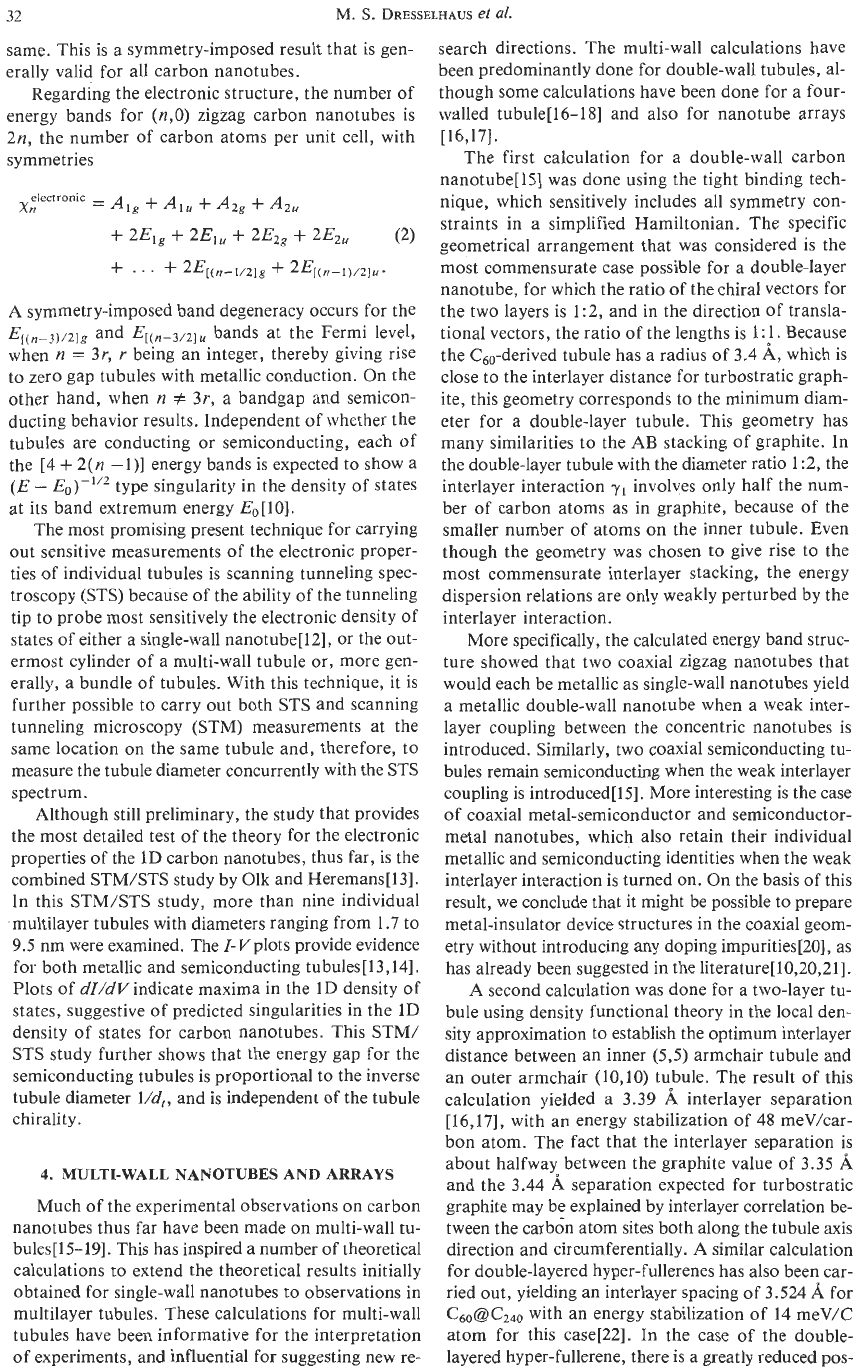
Inspired by experimental observations
on
bundles
of carbon nanotubes, calculations of the electronic
structure have also been carried out
on
arrays of
(6,6)
armchair nanotubes to determine the crystalline struc-
ture
of
the arrays, the relative orientation
of
adjacent
nanotubes, and the optimal spacing between them.
Figure
5
shows one tetragonal and two hexagonal ar-
rays that were considered, with space group symme-
tries P4,/mmc
(DZh)h),
P6/mmm
(Dih),
and P6/mcc
(D,‘,),
respectively[16,17,30]. The calculation shows
Fig.
5.
Schematic representation
of
arrays
of
carbon
nano-
tubes with a common tubule axial direction in the
(a)
tetrag-
onal, (b) hexagonal
I,
and
(c)
hexagonal
I1
arrangements.
The
reference nanotube is generated using
a
planar
ring
of
twelve
carbon atoms arranged
in
six pairs with the
Dsh
symmetry
[16,17,30].
34
M.
S.
DRESSELHAUS et
al.
that the hexagonal
PG/mcc
(D&)
space group has the
lowest energy, leading to
a
gain in cohesive energy
of
2.4 meV/C atom. The orientational alignment between
tubules leads to an even greater gain in cohesive en-
ergy (3.4 eV/C atom), The optimal alignment between
tubules relates closely to the ABAB stacking of graph-
ite, with an inter-tubule separation of 3.14
A
at clos-
est approach, showing that the curvature
of
the
tubules lowers the minimum interplanar distance (as
is
also
found for fullerenes where the corresponding
distance is
2.8
A).
The importance of the inter-tubule
interaction can be seen in the reduction in the inter-
tubule closest approach distance to 3.14
A
for the
P6/mcc
(D,",)
structure, from 3.36
A
and 3.35
A,
re-
spectively, for the tetragonal P42/mmc
(D&)
and
P6/mmm
(D&)
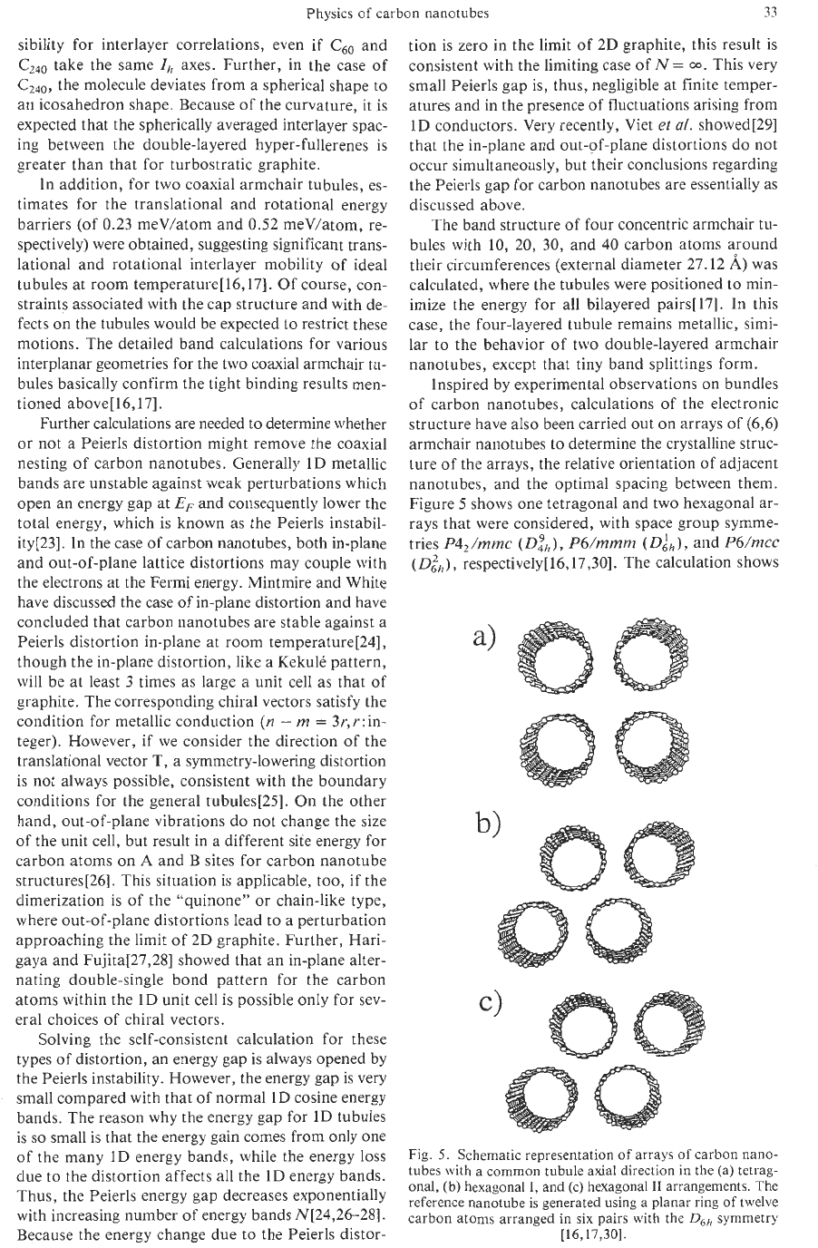
space groups. A plot
of
the electron
dispersion relations for the most stable case is given
in
Fig. 6[16,17,30], showing the metallic nature of this
tubule array by the degeneracy point between the
H
and
K
points in the Brillouin zone between the valence
and conduction bands. It is expected that further cal-
culations will consider the interactions between nested
nanotubes having different symmetries, which
on
physical grounds should interact more weakly, because
of a lack of correlation between near neighbors.
Modifications of the conduction properties of
semiconducting carbon nanotubes by
B
(p-type) and
N
(n-type) substitutional doping has also been dis-
cussed[3 11 and, in addition, electronic modifications
by filling the capillaries of the tubes have also been
proposed[32]. Exohedral doping of the space between
nanotubes in a tubule bundle could provide yet an-
KT
AH
KM
LHrMAL
Fig.
6.
Self-consistent band structure
(48
valence and
5
con-
duction bands) for the hexagonal
I1
arrangement of nano-
tubes, calculated along different high-symmetry directions in
the Brillouin zone. The Fermi Ievel is positioned at the de-
generacy point appearing between
K-H,
indicating metallic
behavior
for
this tubule array[l7].
other mechanism for doping the tubules. Doping
of
the nanotubes by insertion of an intercalate species
between the layers
of
the tubules seems unfavorable
because the interlayer spacing is too small to accom-
modate an intercalate layer without fracturing the
shells within the nanotube.
No
superconductivity has yet been found in carbon
nanotubes or nanotube arrays. Despite the prediction
that 1D electronic systems cannot support supercon-
ductivity[33,34], it is not clear that such theories are
applicable to carbon nanotubes, which are tubular
with
a
hollow core and have several unit cells around
the circumference. Doping
of
nanotube bundles by the
insertion of alkali metal dopants between the tubules
could lead to superconductivity. The doping of indi-
vidual tubules may provide another possible approach
to superconductivity for carbon nanotube systems.
5.
DISCUSSION
This journal issue features the many unusual prop-
erties
of
carbon nanotubes. Most of these unusual
properties are a direct consequence of their
1D
quan-
tum behavior and symmetry properties, including their
unique conduction properties[l 11 and their unique vi-
brational spectra[8].
Regarding electrical conduction, carbon nanotubes
show the unique property that the conductivity can be
either metallic or semiconducting, depending on the
tubule diameter
dt
and chiral angle
0.
For carbon
nanotubes, metallic conduction can be achieved with-
out the introduction of doping or defects. Among the
tubules that are semiconducting, their band gaps ap-
pear to be proportional to
l/d[,
independent of the
tubule chirality. Regarding lattice vibrations, the num-
ber
of
vibrational normal modes increases with
in-
creasing diameter, as expected. Nevertheless, following
from the
1D
symmetry properties
of
the nanotubes,
the number
of
infrared-active and Raman-active modes
remains independent
of
tubule diameter, though the
vibrational frequencies for these optically active modes
are sensitive to tubule diameter and chirality[8]. Be-
cause
of
the restrictions
on
momentum transfer be-
tween electrons and phonons in the electron-phonon
interaction for carbon nanotubes, it has been predicted
that the interaction between electrons and longitudi-
nal phonons gives rise
only
to
intraband scattering and
not interband scattering. Correspondingly, the inter-
action between electrons and transverse phonons gives
rise only to interband electron scattering and not to
intraband scattering[35].
These properties are illustrative
of
the unique be-
havior of 1D systems on
a
rolled surface and result
from the group symmetry outlined in this paper. Ob-
servation of
ID
quantum effects in carbon nanotubes
requires study
of
tubules
of
sufficiently small diameter
to exhibit measurable quantum effects and, ideally,
the measurements should be made
on
single nano-
tubes, characterized for their diameter and chirality.
Interesting effects can be observed in carbon nano-
tubes for diameters in the range 1-20 nm, depending
Physics
of
carbon nanotubes
35
on
the property under investigation.
To
see 1D effects,
faceting should be avoided, insofar as facets lead to
2D behavior, as in graphite.
To
emphasize the possi-
bility of semiconducting properties in non-defective
carbon nanotubes, and to distinguish between conduc-
tors and semiconductors of similar diameter, experi-
ments should be done
on nanotubes of the smallest
possible diameter,
To
demonstrate experimentally the
high density of electronic states expected for
1D
sys-
tems, experiments should ideally be carried
out
on
single-walled tubules
of
small diameter. However, to
demonstrate magnetic properties in carbon nanotubes
with a magnetic field normal to the tubule axis, the tu-
bule diameter should be large compared with the Lan-
dau radius and, in this case, a tubule size of
-
10
nm
would be more desirable, because the magnetic local-
ization within the tubule diameter would otherwise
lead
to
high field graphitic behavior.
The ability of experimentalists to study 1D quan-
tum behavior in carbon nanotubes would be greatly
enhanced if the purification of carbon tubules in the
synthesis process could successfully separate tubules
of a given diameter and chirality.
A new method for
producing mass quantities of carbon nanotubes under
controlled conditions would be highly desirable, as
is now the case for producing commercial quantities
of
carbon fibers. It is expected that nano-techniques
for manipulating very small quantities of material of
nm size[14,36] will
be
improved through research
of
carbon nanotubes, including research capabilities in-
volving the
STM
and
AFM
techniques.
Also
of inter-
est will be the bonding
of
carbon nanotubes to the
other surfaces, and the preparation
of
composite or
multilayer systems that involve carbon nanotubes. The
unbelievable progress in the last 30 years of semicon-
ducting physics and devices inspires our imagination
about future progress in
1D
systems, where carbon
nanotubes may become
a
benchmark material for
study
of
1D systems about a cylindrical surface.
Acknowledgements-We gratefully acknowledge stimulating
discussions with
T.
W.
Ebbesen, M. Endo, and R. A. Jishi.
We are also in debt
to
many colleagues for assistance. The
research at
MIT
is
funded by NSF grant
DMR-92-01878.
One
of the authors (RS) acknowledges the Japan Society for the
Promotion of Science for supporting part of his joint research
with
MIT.
Part of the work by RS is supported by a Grant-
in-Aid
for
Scientific Research in Priority Area “Carbon
Cluster” (Area
No.
234/05233214)
from the Ministry of Ed-
ucation, Science and Culture, Japan.
REFERENCE§
1.
S.
Iijima, Nature (London)
354,
56
(1991).
2.
T.
W.
Ebbesen and
2’.
M.
Ajayan, Nature (London)
358,
220 (1992).
3.
T.
W.
Ebbesen, H. Hiura,
J.
Fujita,
Y.
Ochiai,
S.
Mat-
sui, and K. Tanigaki, Chem. Phys. Lett.
209,
83 (1993).
4.
D.
S.
Bethune,
C.
H. Kiang, M.
S.
deVries,
G.
Gorman,
R. Savoy, J. Vazquez, and
R.
Beyers, Nature
(London)
363, 605 (1993).
5.
S.
Iijima and
T.
Ichihashi, Nature (London)
363,
603
(1993).
6.
M.
S.
Dresselhaus,
G.
Dresselhaus, and
R.
Saito, Phys.
Rev. B
45, 6234 (1992).
7.
R. A. Jishi, M.
S.
Dresselhaus, and
G.
Dresselhaus,
Phys. Rev.
B
47,
16671 (1993).
8.
P.
C.
Eklund, J. M. Holden, and R.
A.
Jishi, Carbon
33,
959 (1995).
9.
R. A. Jishi, L. Venkataraman, M.
S.
Dresselhaus, and
G.
Dresselhaus, Chem. Phys. Lett.
209, 77 (1993).
10.
Riichiro Saito, Mitsutaka Fujita, G. Dresselhaus, and M.
S.
Dresselhaus, Mater.
Sci.
Engin.
B19,
185 (1993).
11.
J.
W.
Mintmire and C.
T.
White,
Carbon
33,
893 (1995).
12.
S.
Wang and D. Zhou,
Chem.
Phys. Lett.
225, 165
13.
14.
15.
16.
17.
18.
19.
20.
21.
22.
23.
24.
25.
26.
27.
28.
29.
(1994).
C. H. Olk and
J.
P.
Heremans,
J.
Mater. Res.
9,
259
(1 994).
J.
P. Issi et al., Carbon
33,
941 (1995).
R.
Saito, G. Dresselhaus, and
M.
S. Dresselhaus,
J.
Appl.
Phys.
73, 494 (1993).
J.
C. Charlier and
J.
P.
Michenaud, Phys. Rev. Lett.
70,
1858
(1993).
J.
C.
Charlier, Carbon Nunotubes and Fullerenes. PhD
thesis, Catholic University of Louvain, Department
of
Physics, May
1994.
Ph. Lambin, L. Philippe, J.
C.
Charlier, and
J.
P.
Michenaud,
Comput.
Muter. Sei.
2,
350 (1994).
Ph. Lambin, L. Philippe,
J.
C. Charlier, and
J.
P.
Michenaud,
In
Proceedings
of
the Winter School
on
Ful-
lerenes (Edited by H. Kuzmany, J. Fink,
M.
Mehring,
and
S.
Roth), Kirchberg Winter School, Singapore,
World Scientific Publishing Co., Ltd.
(1994).
R.
Saito,
M.
Fujita,
G.
Dresselhaus, and
M.
S.
Dressel-
haus, Appl. Phys. Lett.
60,
2204 (1992).
M.
S.
Dresselhaus,
G.
Dresselhaus, and Riichiro Saito,
Mater. Sei. Engin.
B19,
122 (1993).
Y. Yosida, Fullerene
Sci.
Tech.
I,
55 (1993).
R. E. Peierls,
In
Quantum Theory
of
Solids.
London,
Oxford University Press
(1955).
J.
W.
Mintmire, Phys. Rev
B
43,
14281
(June
1991).
Kikuo Harigaya, Chem. Phys. Lett.
189,
79 (1992).
R.
Saito, M. Fujita,
G.
Dresselhaus, and M.
S.
Dressel-
haus,
In
Electrical, Optical and Magnetic Properties
of
Organic Solid State Materials, MRS Symposia Proceed-
ings, Boston. Edited by L.
Y.
Chiang,
A.
F.
Garito, and
D. J. Sandman, vol.
247,
p.
333,
Pittsburgh,
PA,
Ma-
terials Research Society Press
(1992).
K.
Harigaya and M. Fujita, Phys. Rev.
B
47,
16563
(1
993).
K.
Harigaya and M: Fujita, Synth. Metals
55,
3196
(1993).
N.
A.
Viet, H. Ajiki, and
T.
Ando, ISSP Technical Re-
oorf
2828
(1994).
~I
30.
J. C. Charlier,
X.
Gonze,
and J.
P.
Michenaud, Euro-
31.
J.
Y.
Yi and
J.
Bernholc, Phys. Rev.
B47,
1708 (1993).
32.
T.
W.
Ebbesen,
Annu.
Rev.
Mater. Sei.
24, 235 (1994).
33.
H.
Frohlich, Phys. Rev.
79, 845 (1950).
34.
H. Frohlich, Proc. Roy.
SOC.
London
A215,
291 (1952).
35.
R.
A.
Jishi,
M.
S. Dresselhaus, and
G.
Dresselhaus,
Phys. Rev.
B
48,
11385 (1993).
36.
L.
Langer,
L.
Stockman,
J.
P.
Heremans,
V.
Bayot,
C. H. Olk,
C.
Van Haesendonck,
Y.
Bruynseraede,
and
J.
P. Issi,
J.
Mat.
Res.
9, 927 (1994).
phys. Lett.
29, 43 (1994).
ELECTRONIC AND STRUCTURAL PROPERTIES
OF
CARBON NANOTUBES
J.
W.
MINTMIRE
and
C.
T.
WHITE
Chemistry Division, Naval Research Laboratory, Washington,
DC
20375-5342,
U.S.A.
(Received
12
October
1994;
accepted in revised form
15
February
1995)
Abstract-Recent developments using synthetic methods typical of fullerene production have
been
used
to generate graphitic nanotubes with diameters
on
the
order of fullerene diameters: “carbon nanotubes.”
The individual hollow concentric graphitic nanotubes
that
comprise these fibers can be visualized as
con-
structed from rolled-up single sheets
of
graphite.
We
discuss the use of helical symmetry for
the
electronic
structure of
these
nanotubes, and the resulting trends we observe
in
both band gap and strain energy ver-
sus
nanotube
radius,
using
both
empirical and
first-principles
techniques. With potential
electronic
and
structural applications,
these
materials appear to
be
appropriate
synthetic
targets for
the current
decade.
Key
Words-Carbon nanotube,
electronic
properties,
structural
properties,
strain
energy,
band
gap,
band
structure, electronic
structure.
1.
INTRODUCTION
Less than four years ago Iijima[l] reported the novel
synthesis based on the techniques used for fullerene
synthesis[2,3] of substantial quantities of multiple-shell
graphitic nanotubes with diameters of nanometer di-
mensions. These nanotube diameters were more than
an order
of
magnitude smaller than those typically ob-
tained using routine synthetic methods for graphite fi-
bers[4,5]. This work has been widely confirmed in the
literature, with subsequent work by Ebbesen and
Ajayan[6] demonstrating the synthesis of bulk quan-
tities of these materials. More recent work
has
further
demonstrated the synthesis of abundant amounts
of
single-shell graphitic nanotubes with diameters on the
order of one nanometer[7-9]. Concurrent with these
experimental studies, there have been many theoreti-
cal studies of the mechanical and electronic properties
of these novel fibers[lO-30]. Already, theoretical stud-
ies of the individual hollow concentric graphitic nano-
tubes, which comprise these fibers, predict that these
nanometer-scale diameter nanotubes will exhibit con-
ducting properties ranging from metals to moderate
bandgap semiconductors, depending
on
their radii and
helical structure[lO-221. Other theoretical studies have
focused on structural properties and have suggested
that these nanotubes could have high strengths and
rigidity resulting from their graphitic and tubular
structure[23-30]. The metallic nanotubes- termed ser-
pentine[23] -have also been predicted to be stable
against
a
Peierls distortion
to
temperatures far below
room temperaturejl01. The fullerene nanotubes show
the promise of an array of all-carbon structures that
exhibits a broad range of electronic and structural
properties, making these materials an important syn-
thetic target for the current decade.
Herein, we summarize some of the basic electronic
and structural properties expected of these nanotubes
from theoretical grounds. First we will discuss the ba-
sic structures
of
the nanotubes, define the nomencla-
ture used in the rest of the manuscript, and present an
analysis of the rotational
and
helical symmetries
of
the
nanotube. Then, we will discuss the electronic struc-
ture of the nanotubes in terms of applying Born-von
Karman boundary conditions
to
the two-dimensional
graphene sheet. We will then discuss changes intro-
duced by treating the nanotube realistically as a three-
dimensional system with helicity, including results
both from all-valence empirical tight-binding results
and first-principles local-density functional
(LDF)
results.
2.
NANOTUBE
STRUCTURE
AND SYMMETRY
Each single-walled nanotube can be viewed as a
conformal mapping
of
the two-dimensional lattice of
a
single sheet of graphite (graphene), depicted as the
honeycomb lattice of a single layer of graphite in Fig.
1,
onto the surface of a cylinder.
As
pointed
out
by
Iijima[
11,
the proper boundary conditions around the
cylinder can only be satisfied
if
one of the Bravais lat-
tice vectors of the graphite sheet maps to a circumfer-
ence around the cylinder.
Thus,
each real lattice vector
of the two-dimensional hexagonal lattice (the Bravais
lattice for the honeycomb) defines a different way of
rolling up the sheet into
a
nanotube. Each such lattice
vector,
E,
can be defined in terms of the two primi-
tive lattice vectors
RI
and
R2
and
a
pair
of
integer in-
dices [n,,nz], such that
B
=nlR1
+
n2R2,
with Fig.
2
depicting an example for
a
[4,3] nanotube. The point
group symmetry of the honeycomb lattice will make
many of these equivalent, however,
so
truly unique
nanotubes are only generated using a one-twelfth ir-
reducible wedge of the Bravais lattice. Within this
wedge, only a finite number of nanotubes can be con-
structed with a circumference below any given value.
The construction of the nanotube from a confor-
mal mapping
of
the graphite sheet shows that each
nanotube can have up
to
three inequivalent (by point
37