Endo M., Iijima S., Dresselhaus M.S. (eds.) Carbon nanotubes
Подождите немного. Документ загружается.

8 M. ENDO
et
al.
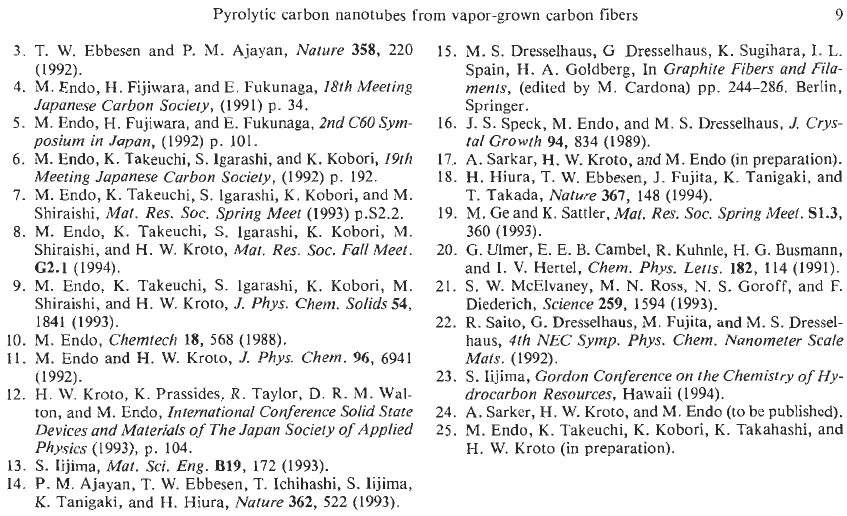
of ca. 10 nm (white arrow), observed by field emission
scanning electron microscopy (FE-SEM)[25]. It is,
thus, suggested that at least some of the VGCFs start
as nanotube cores, which act as
a
substrate for sub-
sequent thickening by deposition of secondary pyro-
lytic carbon material, as in the catalytically primarily
grown hollow fiber. In Fig. 14b is also shown the TEM
image corresponding to the extruded nanotube from
a
very thin fiber. It is clearly observed that the exposed
nanotube is continuing into the fiber as
a
central hol-
low core, as indicated by the white arrow in the figure.
It is interesting that, as indicated before (in Fig. 14a),
the core is more flexible than the pyrolytic part, which
is more fragile.
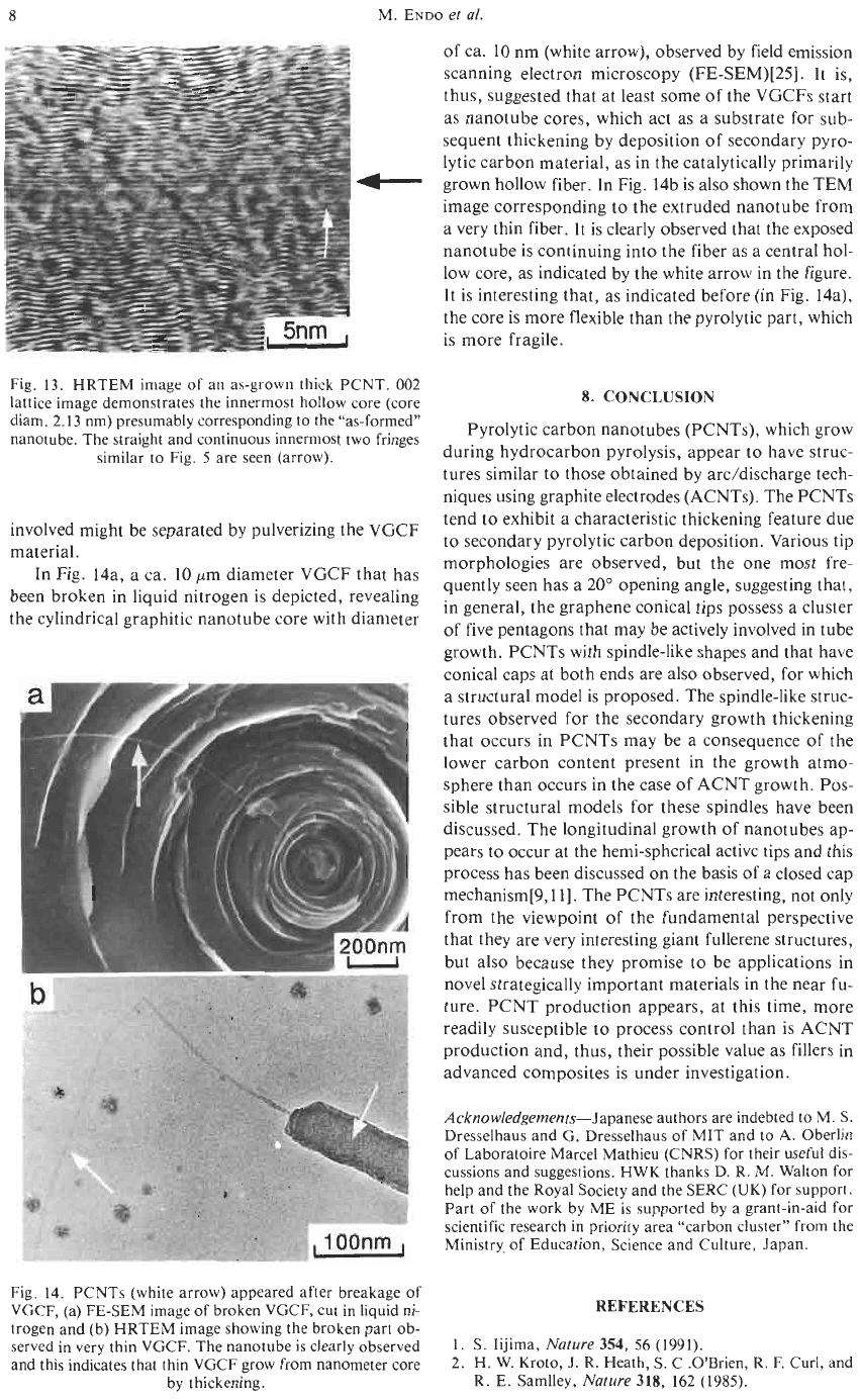
Fig. 13. HRTEM image of an as-grown thick PCNT.
002
lattice image demonstrates the innermost hollow core (core
diam. 2.13 nm) presumably corresponding to the “as-formed”
nanotube. The straight and continuous innermost two fringes
similar to Fig. 5 are seen (arrow).
Pyrolytic carbon nanotubes (PCNTs), which grow
during hydrocarbon pyrolysis, appear to have struc-
tures similar to those obtained by arddischarge tech-
niques using graphite electrodes (ACNTs). The PCNTs
involved might be separated by pulverizing the VGCF
material.
In Fig. 14a, a ca.
10
wm diameter VGCF that has
been broken in liquid nitrogen is depicted, revealing
the cylindrical graphitic nanotube core with diameter
8.
CONCLUSION
tend to exhibit
a
characteristic thickening feature due
to secondary pyrolytic carbon deposition. Various tip
morphologies are observed, but the one most fre-
quently seen has a 20” opening angle, suggesting that,
in general, the graphene conical tips possess a cluster
of five pentagons that may be actively involved in tube
growth. PCNTs with spindle-like shapes and that have
conical caps at both ends are also observed, for which
a
structural model is proposed. The spindle-like struc-
tures observed for the secondary growth thickening
that occurs in PCNTs may be
a
consequence of the
lower carbon content present in the growth atmo-
sphere than occurs in the case of ACNT growth.
Pos-
sible structural models for these spindles have been
discussed. The longitudinal growth of nanotubes ap-
pears to occur at the hemi-spherical active tips and this
process has been discussed on the basis of
a
closed cap
mechanism[9,11]. The PCNTs are interesting, not only
from the viewpoint of the fundamental perspective
that they are very interesting giant fullerene structures,
but also because they promise to be applications in
novel strategically important materials in the near fu-
ture. PCNT production appears, at this time, more
readily susceptible to process control than is ACNT
production and, thus, their possible value as fillers in
advanced composites is under investigation.
Acknowledgements-Japanese authors are indebted to M.
S.
Dresselhaus and G. Dresselhaus of MIT and to
A.
Oberlin
of Laboratoire Marcel Mathieu (CNRS) for their useful dis-
cussions and suggestions. HWK thanks D. R. M. Walton for
help and the Royal Society and the SERC (UK) for support.
Part of the work by ME is supported by a grant-in-aid for
scientific research in priority area “carbon cluster” from the
Ministry. of Education, Science and Culture, Japan.
Fig. 14. PCNTs (white arrow) appeared after breakage of
VGCF, (a) FE-SEM image of broken VGCF, cut in liquid ni-
trogen and (b) HRTEM image showing the broken part ob-
served in very thin VGCF. The nanotube is clearly observed
and this indicates that thin VGCF grow from nanometer core
by thickening.
REFERENCES
1.
S.
Iijima,
Nature
354,
56 (1991).
2. H. W. Kroto, J. R. Heath,
S.
C .O’Brien, R. F.
Curl,
and
R. E. Samlley,
Nature
318,
162 (1985).
Pyrolytic carbon nanotubes from vapor-grown carbon fibers
9
3.
T.
W. Ehhesen and
P.
M.
Ajayan,
Nature
358,
220
(1
992).
4.
M.
Endo,
H.
Fijiwara, and E. Fukunaga,
18th Meeting
Japanese Carbon Society,
(1991)
p.
34.
5.
M. Endo,
H.
Fujiwara, and E. Fukunaga,
2nd
C60
Sym-
posium in Japan,
(1992)
p.
101.
6.
M. Endo, K. Takeuchi,
S.
Igarashi, and K. Kobori,
19th
Meeting Japanese Carbon Society,
(1992)
p.
192.
7.
M.
Endo, K. Takeuchi,
S.
Igarashi, K. Kobori, and M.
Shiraishi,
Mat. Res.
SOC.
Spring Meet
(1993) p.S2.2.
8.
M.
Endo,
K.
Takeuchi,
S.
Igarashi,
K.
Kobori,
M.
Shiraishi, and H.
W.
Kroto,
Mat. Res.
SOC.
FallMeet.
62.1 (1994).
9.
M. Endo, K. Takeuchi,
S.
Igarashi,
K.
Kobori, M.
Shiraishi, and H.
W.
Kroto,
J.
Phys. Chem. Solids
54,
1841 (1993).
10.
M.
Endo,
Chemtech
18,
568 (1988).
11.
M.
Endo
and
H.
W.
Kroto,
J.
Phys. Chem.
96,
6941
(1992).
12.
I-I.
W. KrOtQ,
K.
Prassides,
R.
Taylor, D.
R.
M.
Wal-
ton, and
bd.
Endo,
International Conference Solid State
Devices and Materials
of
The
Japan
Society
of
Applied
Physics
(1993),
p.
104.
13.
S.
Iijima,
Mat. Sci. Eng.
B19,
172 (1993).
14.
P.
M.
Ajayan,
T.
W.
Ebbesen,
T.
Ichihashi,
S.
Iijirna,
K. Tanigaki, and H. Hiura,
Nature
362,
522 (1993).
15.
M.
S.
Dresselhaus,
G
Dresselhaus, K. Sugihara,
I.
L.
Spain,
H.
A.
Goldberg, In
Graphite Fibers and Fila-
ments,
(edited by
M.
Cardona) pp.
244-286.
Berlin,
Springer.
16.
J.
S. Speck, M. Endo, and
M.
S.
Dresselhaus,
J.
Crys-
tal Growth
94,
834 (1989).
17..
A. Sarkar,
H.
W.
Kroto, and M. Endo (in preparation).
18.
H. Hiura,
T.
W.
Ebbesen,
J.
Fujita,
K.
Tanigaki, and
T.
Takada,
Nature
367, 148 (1994).
19.
M.
Ge and
K.
Sattler,
Mat. Res. SOC. Spring Meet.
S1.3,
360 (1993).
20.
G.
Ulmer,
E.
E.
B.
Cambel,
R.
Kuhnle,
H.
G.
Busmann,
and
1.
V.
Hertel,
Chem. Phys. Letts.
182,
114 (1991).
21.
S.
W.
McElvaney, M.
N.
Ross,
N.
S.
Goroff, and
E
Diederich,
Science
259,
1594 (1993).
22.
R.
Saito,
G.
Dresselhaus,
M.
Fujita, and M.
S.
Dressel-
haus,
4th NEC Symp. Phys. Chem. Nanometer Scale
Mats.
(1992).
23.
S.
Iijima,
Gordon Conference
on
the Chemistry of Hy-
drocarbon Resources,
Hawaii
(1994).
24.
A.
Sarker,
H.
W.
Kroto, and
M.
Endo (to he published).
25.
M.
Endo,
K.
Takeuchi, K. Kobori,
K.
Takahashi, and
H.
W.
Kroto (in preparation).
ELECTRIC EFFECTS IN
NANOTUBE
GROWTH
DANIEL
T.
COLBERT
and
RICHARD
E.
SMALLEY
Rice Quantum Institute and Departments
of
Chemistry and Physics,
MS
100,
Rice University, Houston,
TX
77251-1892,
U.S.A.
(Received
3
April
1995;
accepted
7
April
1995)
Abstract-We
present
experimental
evidence
that strongly
supports
the hypothesis
that
the
electric
field
of
the
arc
plasma
is
essential
for
nanotube growth
in
the
arc
by
stabilizing
the
open
tip
structure
against
closure.
By
controlling
the
temperature and bias voltage applied to a single nanotube mounted on a mac-
roscopic electrode,
we
find that the nanotube tip closes when heated to a temperature similar
to
that in
the arc
unless
an
electric field is applied.
We
have
also
developed a more refined awareness of “open”
tips in which adatoms bridge between edge atoms
of
adjacent layers, thereby lowering the exothermicity
in going from the open to the perfect dome-closed tip. Whereas realistic fields appear to be insufficient
by
themselves to stabilize
an
open tip with its edges completely exposed, the field-induced energy lower-
ing
of
a
tip
having adatom spot-welds can, and indeed
in
the
arc
does,
make
the
open
tip
stable relative
to
the
closed
one.
Key
Words-Nanotubes,
electric
field,
arc plasma
1.
INTRODUCTION
As recounted throughout this special issue, significant
advances in illuminating various aspects of nanotube
growth have been made[l,2] since Iijima’s eventful
discovery in
1991;[3]
these advances are crucial to
gaining control over nanotube synthesis, yield, and
properties such as length, number of layers, and he-
licity. The carbon arc method Iijima used remains the
principle method of producing bulk amounts of qual-
ity nanotubes, and provides key clues for their growth
there and elsewhere. The bounty of nanotubes depos-
ited on the cathode (Ebbesen and Ajayan have found
that up
to
50%
of
the deposited carbon is tubular[4])
is particularly puzzling when one confronts the evi-
dence of UgarteI.51 that tubular objects are energeti-
cally less stable than spheroidal onions.
It
is
largely accepted that nanotube growth occurs
at
an
appreciable rate
only
at open tips. With this con-
straint, the mystery over tube growth in the arc redou-
bles when one realizes that the cathode temperature
(-3000°C)
is well above that required to anneal car-
bon vapor
to
spheroidal closed shells (fullerenes and
onions) with great efficiency. The impetus to close is,
just as for spheroidal fullerenes, elimination of the
dangling bonds that unavoidably exist in any open
structure by incorporation of pentagons into the hex-
agonal lattice. Thus,
a
central question in the growth
of nanotubes in the arc is: How do they stay open?
One
of
us
(RES)
suggested over two years ago161
that the resolution
to
this question lies in the electric
field inherent to the arc plasma.
As
argued then, nei-
ther thermal nor concentration gradients are close to
the magnitudes required to influence tip annealing,
and trace impurities such as hydrogen, which might
keep the tip open, should have almost no chemisorption
residence time at
3000°C.
The fact that well-formed
nanotubes are found only in the cathode deposit, where
the electric field concentrates, and never in the soots
condensed from the carbon vapor exiting the arcing
region, suggest a vital role for the electric field.
Fur-
thermore, the field strength at the nanotube tips is very
large, due both
to
the way the plasma concentrates
most of the potential drop in a very short distance
above the cathode, and to the concentrating effects of
the field at the tips of objects as small as nanotubes.
The field may be on the order of the strength required
to break carbon-carbon bonds, and could thus dra-
matically effect the tip structure.
In the remaining sections of this paper, we describe
the experimental results leading to confirmation of the
stabilizing role of the electric field in arc nanotube
growth. These include: relating the plasma structure
to the morphology of the cathode deposit, which re-
vealed that the integral role of nanotubes in sustain-
ing the arc plasma is their field emission of electrons
into the plasma; studying the field emission character-
istics of isolated, individual arc-grown nanotubes; and
the discovery of a novel production of nanotubes that
significantly alters the image of the “open” tip that the
arc electric field keeps from closing.
2.
NANOTUBES
AS
FIELD
EMITTERS
Defects in arc-grown nanotubes place limitations
on their utility. Since defects appear to arise predom-
inantly due to sintering of adjacent nanotubes in the
high temperature
of
the arc, it seemed sensible to
try
to reduce the extent of sintering by cooling the cath-
ode better[2]. The most vivid assay for the extent of
sintering is the oxidative heat purification treatment
of
Ebbesen and coworkers[7], in which amorphous
carbon and shorter nanoparticles are etched away be-
fore nanotubes are substantially shortened. Since, as
we proposed, most of the nanoparticle impurities orig-
11
12
D.
T.
COLBERT
and
R.
E.
SMALLEY
inated as broken fragments of sintered nanotubes, the
amount
of
remaining material reflects the degree of
sintering.
Our examinations
of
oxygen-purified deposits led
to construction of a model of nanotube growth in the
arc in which the nanotubes play an active role in
sus-
taining the arc plasma, rather than simply being a
passive product[2]. Imaging unpurified nanotube-rich
arc deposit from the top by scanning electron micros-
copy (SEM) revealed
a
roughly hexagonal lattice
of
50-micron diameter circles spaced
-50
microns apart.
After oxidative treatment the circular regions were seen
to
have etched away, leaving
a
hole. More strikingly,
when the deposit was etched after being cleaved ver-
tically
to
expose the inside
of
the deposit, SEM imag-
ing showed that columns the diameter
of
the circles
had been etched all the way from the top to the bot-
tom of the deposit, leaving only the intervening mate-
rial. Prior SEM images of the column material (zone 1)
showed that the nanotubes there were highly aligned
in the direction
of
the electric field (also the direction
of deposit growth), whereas nanotubes in the sur-
rounding region (zone
2)
lay in tangles, unaligned with
the field[2]. Since zone
1
nanotubes tend
to
be in much
greater contact with one another, they are far more
susceptible
to
sintering than those in zone
2,
resulting
in the observed preferential oxidative etch of zone
1.
These observations consummated in
a
growth
model that confers on the millions of aligned zone
1
nanotubes the role of field emitters, a role they play
so
effectively that they are the dominant source of
electron injection into the plasma. In response, the
plasma structure, in which current flow becomes con-
centrated above zone 1, enhances and sustains the
growth of the field emission source-that is, zone
1
nanotubes. A convection cell is set up in order
to
al-
low the inert helium gas, which is swept down by col-
lisions with carbon ions toward zone
1,
to return
to
the plasma. The helium flow carries unreacted carbon
feedstock out of zone
1,
where it
can
add to the grow-
ing zone 2 nanotubes. In the model, it is the size and
spacing of these convection cells in the plasma that de-
termine the spacing of the zone
l
columns in a hex-
agonal lattice.
3.
FIELD
EMISSION FROM
AN
ATOMIC
WIRE
Realization
of
the critical importance played by
emission in our arc growth model added impetus to
investigations already underway to characterize nano-
tube field emission behavior in
a
more controlled man-
ner. We had begun working
with
individual nanotubes
in the hope
of
using them as seed crystals for con-
trolled, continuous growth (this remains an active
goal). This required developing techniques for harvest-
ing nanotubes from arc deposits, and attaching them
with good mechanical and electrical connection to
macroscopic manipulators[2,8,9]. The resulting nano-
electrode was then placed in a vacuum chamber in
which the nanotube tip could be heated by applica-
tion
of
Ar+-laser light
(514.5
nm) while the potential
bias was controlled relative
to
an opposing electrode,
and if desired, reactive gases could be introduced.
Two classes
of
emission behavior were found. An
inactivated state, in which the emission current in-
creased upon laser heating at a fixed potential bias,
was consistent with well understood thermionic field
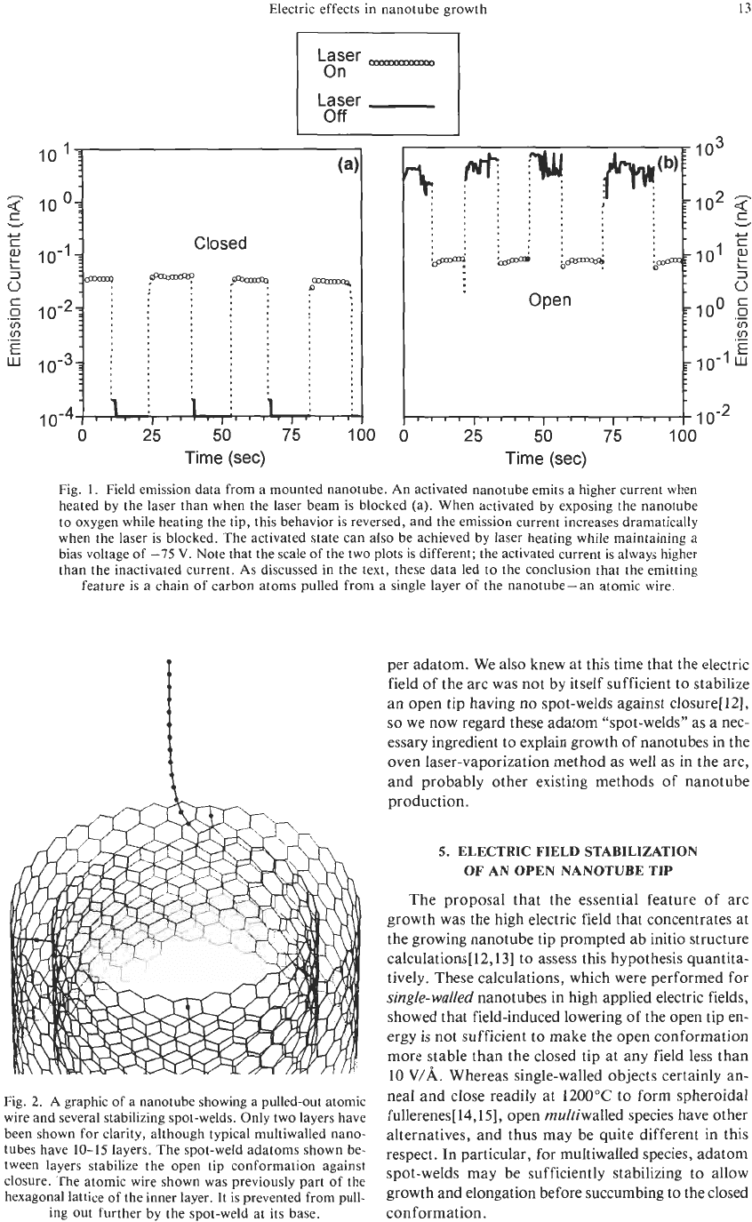
emission models. Figure la displays the emission cur-
rent as the laser beam is blocked and unblocked, re-
vealing a 300-fold thermal enhancement upon heating.
Etching the nanotube tip with oxygen while the tube
was laser heated to
1500°C
and held at
-75
V
bias
produced an activated state with exactly the opposite
behavior, shown in Fig. 2b; the emission current
in-
creased
by nearly two orders of magnitude when the
laser beam was blocked! Once we eliminated the pos-
sibility that species chemisorbed on the tip might be
responsible for this behavior, the explanation had to
invoke a structure built only of carbon whose sharp-
ness would concentrate the field, thus enhancing the
emission current.
As
a result
of
these studies[9], a dra-
matic and unexpected picture has emerged of the
nanotube as field emitter, in which the emitting source
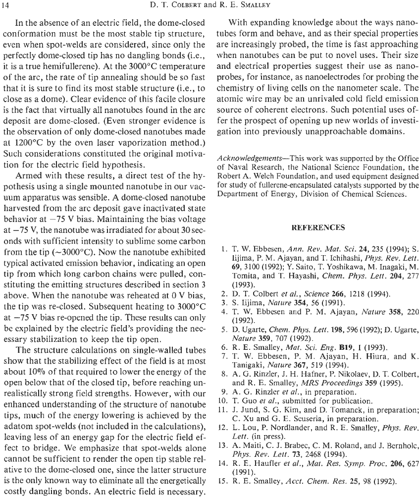
is an atomic wire composed of
a
single chain of car-
bon atoms that has been unraveled from the tip by the
force of the applied electric field (see Fig.
2).
These
carbon wires can be pulled out from the end of the
nanotube only once the ragged edges of the nanotube
layers have been exposed. Laser irradiation causes the
chains
to
be clipped from the open tube ends, result-
ing in low emission when the laser beam is unblocked,
but fresh ones are pulled out once the laser is blocked.
This unraveling behavior is reversible and reproducible.
4.
THE
STRUCTURE
OF
AN OPEN
NANOTUBE
TIP
A portion
of
our
ongoing work focusing on sphe-
roidal fderenes, particularly metallofullerenes, utilized
the same method of production as was originally used
in the discovery of fullerenes, the laser-vaporization
method, except for the modification of placing the
flow tube in an oven to create better annealing con-
ditions for fullerene formation. Since we knew that at
the typical
1200°C
oven temperature, carbon clusters
readily condensed and annealed to spheroidal fuller-
enes (in yields close to
40%),
we were astonished to
find, upon transmission electron micrographic exam-
ination of the collected soots, multiwalled nanotubes
with few or no defects up to
300
nm
long[lO]! How,
we asked ourselves, was it possible for
a
nanotube
precursor
to
remain open under conditions known
to
favor its closing, especially considering the absence of
extrinsic agents such as
a
strong electric field, metal
particles, or impurities
to
hold the tip open for growth
and elongation?
The only conclusion we find tenable is that an
in-
trinsic
factor of the nanotube was stabilizing it against
closure, specifically, the bonding of carbon atoms to
edge atoms of adjacent layers, as illustrated in Fig.
2.
Tight-binding calculations[l 1
J
indicate that such sites
are energetically preferred over direct addition to the
hexagonal lattice
of
a single layer by as much as
1.5
eV
Electric effects in nanotube growth
13
Laser
On
Laser
Off
10
0
25
50
75 100
Time (sec) Time (sec)
Fig.
1.
Field emission data from a mounted nanotube. An activated nanotube emits a higher current when
heated by the laser than when the laser beam is blocked (a). When activated by exposing the nanotube
to oxygen while heating the tip, this behavior is reversed, and the emission current increases dramatically
when the laser is blocked. The activated state can also be achieved by laser heating while maintaining
a
bias voltage of
-75
V.
Note that the scale of the two plots is different; the activated current is always higher
than the inactivated current. As discussed in the text, these data led to the conclusion that the emitting
feature is a chain of carbon atoms pulled from a single layer of the nanotube-an atomic wire.
per adatom. We also knew at this time that the electric
field of the arc was not by itself sufficient to stabilize
an open tip having no spot-welds against closure[l2],
so
we now regard these adatom "spot-welds'' as a nec-
essary ingredient to explain growth of nanotubes in the
oven laser-vaporization method as well as in the arc,
and probably other existing methods
of
nanotube
production.
5.
ELECTRIC FIELD STABILIZATION
OF
AN
OPEN NANOTUBE
TIP
The proposal that the essential feature of arc
growth was the high electric field that concentrates at
the growing nanotube tip prompted ab initio structure
calculations[ 12,131 to assess this hypothesis quantita-
tively. These calculations, which were performed for
single-walled nanotubes in high applied electric fields,
showed that field-induced lowering of the open tip en-
ergy is not sufficient to make the open conformation
more stable than the closed tip at any field less than
10
V/A.
Whereas single-walled objects certainly an-
neal
and
at
12000c
t'
form
'pheroidal
fullerenes[l4,151, open multiwalled species have other
alternatives, and thus may be auite different in this
Fig.
2.
A graphic
of
a nanotube showing
a
pulled-out atomic
wire and several stabilizing spot-welds. Only two layers have
been shown for clarity, although typical multiwalled nano-
tubes have
10-15
layers. The spot-weld adatoms shown be-
tween layers stabilize the open tip conformation against
closure. The atomic wire shown was previously part
of
the
hexagonal lattice
of
the inner layer. It is prevented from pull-
respect. In particular, for multiwalled species, adatom
spot-welds
may
be sufficiently stabilizing to allow
growth
and before
succumbing
to
the
ing out further by the spot-weld at its base.
conformation.
14
D.
T.
COLBERT and R.
E.
SMALLEY
In the absence of an electric field, the dome-closed
conformation must be the most stable tip structure,
even when spot-welds are considered, since only the
perfectly dome-closed tip has
no
dangling bonds (Le.,
it
is
a
true hemifullerene). At the
3000°C
temperature
of
the arc, the rate
of
tip annealing should be
so
fast
that it is sure to find its most stable structure (i.e., to
close as a dome). Clear evidence of this facile closure
is the fact that virtually all nanotubes found in the arc
deposit are dome-closed. (Even stronger evidence is
the observation of only dome-closed nanotubes made
at
1200°C
by the oven laser vaporization method.)
Such considerations constituted the original motiva-
tion for the electric field hypothesis.
Armed with these results, a direct test of the hy-
pothesis using
a
single mounted nanotube in our vac-
uum
apparatus was sensible. A dome-closed nanotube
harvested from the arc deposit gave inactivated state
behavior
at
-75
V
bias. Maintaining the bias voltage
at
-75 V,
the nanotube was irradiated for about
30
sec-
onds with sufficient intensity to sublime some carbon
from the tip
(-3000°C).
Now the nanotube exhibited
typical activated emission behavior, indicating an open
tip from which long carbon chains were pulled, con-
stituting the emitting structures described in section
3
above. When the nanotube was reheated at
0
V
bias,
the tip was re-closed. Subsequent heating to
3000°C
at
-75
V
bias re-opened the tip. These results can only
be explained by the electric field’s providing the nec-
essary stabilization to keep the tip open.
The structure calculations on single-walled tubes
show that the stabilizing effect
of
the field is at most
about
10%
of that required to lower the energy of the
open below that of the closed tip, before reaching un-
realistically strong field strengths. However, with our
enhanced understanding
of
the structure
of
nanotube
tips, much of the energy lowering is achieved by the
adatom spot-welds (not included in the calculations),
leaving less
of
an energy gap for the electric field ef-
fect
to
bridge. We emphasize that spot-welds alone
cannot be sufficient to render the open tip stable rel-
ative to the dome-closed one, since the latter structure
is the only known way to eliminate
all
the energetically
costly dangling bonds. An electric field is necessary.
With expanding knowledge about the ways nano-
tubes form and behave, and as their special properties
are increasingly probed, the time is fast approaching
when nanotubes can be put to novel uses. Their size
and electrical properties suggest their use
as
nano-
probes, for instance, as nanoelectrodes for probing the
chemistry of living cells
on
the nanometer scale. The
atomic wire may be an unrivaled cold field emission
source
of
coherent electrons. Such potential uses of-
fer the prospect
of
opening up new worlds of investi-
gation into previously unapproachable domains.
Acknowledgements-This
work was supported by the Office
of Naval Research, the National Science Foundation, the
Robert
A.
Welch Foundation, and used equipment designed
for
study
of
fullerene-encapsulated catalysts supported by the
Department of Energy, Division
of
Chemical Sciences.
REFERENCES
1.
T.
W. Ebbesen,
Ann.
Rev. Mat.
Sei.
24, 235 (1994); S.
Iijima,
P.
M.
Ajayan, and
T.
Ichihashi,
Phys. Rev. Lett.
69, 3100 (1992);
Y.
Saito,
T.
Yoshikawa,
M.
Inagaki,
M.
Tomita, and
T.
Hayashi,
Chem. Phys.
Lett.
204,
277
(1993).
2. D.
T.
Colbert
et
a/.,
Science
266,
1218
(1994).
3.
S.
Iijima,
Nature
354, 56 (1991).
4.
T.
W. Ebbesen and
P.
M. Ajayan,
Nature
358, 220
5.
D. Ugarte,
Chem. Phys. Lett.
198,596 (1992); D. Ugarte,
6.
R.
E. Srnalley,
Mat
Sci.
Eng.
B19,
1 (1993).
7.
T.
W. Ebbesen,
P.
M.
Ajayan,
H.
Hiura, and K.
Tanigaki,
Nature
367,
519 (1994).
8.
A.
G. Rinzler,
J.
H.
Hafner,
P.
Nikolaev, D.
T.
Colbert,
and R.
E.
Srnalley,
MRS Proceedings
359 (1995).
9.
A.
G.
Rinzler
et
al.,
in preparation.
(1992).
Nature
359,
707
(1992).
10.
T.
Guo
et al.,
submitted
for
publication.
11.
J.
Jund,
S.
G.
Kim, and D. Tomanek, in preparation;
12.
L.
Lou,
P.
Nordlander, and
R.
E.
Srnalley,
Phys.
Rev.
13.
A.
Maiti,
C.
J.
Brabec, C.
M.
Roland, and
J.
Bernholc,
14. R.
E.
Haufler
et
al.,
Mat. Res.
Symp.
Proc.
206, 621
15.
R.
E. Srnalley,
Acct. Chem. Res.
25,
98 (1992).
C.
Xu
and
G.
E.
Scuseria, in preparation.
Lett.
(in press).
Phys. Rev. Lett.
13, 2468 (1994).
(1 991).
CATALYTIC PRODUCTION AND PURIFICATION
OF
NANOTUBULES HAVING FULLERENE-SCALE DIAMETERS
V.
I[vANov,~**
A.
FONSECA,"
J. B.NAGY,"+
A.
LUCAS,"
P.
LAMBIN,"
D.
BERNAERTS~
and
X.
B.
ZHANG~
"Institute for Studies
of
Interface Science, FacultCs Universitaires Notre
Dame
de la
Paix,
61
rue
de
Bruxelles, B-5000 Namur, Belgium
bEMAT,
University
of
Antwerp (RUCA), Groenenborgerlaan
171,
B-2020 Antwerp,
Belgium
(Received
25
July
1994;
accepted
in
revisedform
13
March
1995)
Abstract-Carbon nanotubules
were
produced in a
large
amount
by
catalytic decomposition
of
acetylene
in
the
presence
of
various supported transition metal catalysts. The influence
of
different parameters such
as
the
nature
of
the
support,
the
size
of
active metal particles and
the
reaction conditions
on
the
formation
of
nanotubules
was studied. The process was optimized towards
the
production
of
nanotubules
having
the same diameters as the fullerene tubules obtained from the arc-hscharge method. The separation
of
tubules from the substrate, their purification and opening were also investigated.
Key
Words-Nanotubules, fullerenes, catalysis.
1.
INTRODUCTION
The catalytic growth
of
graphitic carbon nanofibers
during the decomposition of hydrocarbons in the
presence of either supported or unsupported metals,
has been widely studied over the last years[ 1-61.
The main goal of these studies was to avoid the
formation of "filamentous" carbon, which strongly
poisons the catalyst. More recently, carbon tubules
of
nanodiameter were found to be a byproduct of
arc-discharge production
of
fullerenes [7]. Their cal-
culated unique properties such as high mechanical
strength[
81,
their capillary properties
[
91
and their
remarkable electronic structure
[
10-121
suggest a
wide range of potential uses in the future. The catalyti-
cally produced filaments can be assumed to be ana-
logous to the nanotubules obtained from arc-
discharge and hence to possess similar properties
[
51,
they can also be used as models
of
fullerene nano-
tubes. Moreover, advantages over arc-discharge fibers
include a much larger length (up to
50pm)
and a
relatively low price because of simpler preparation.
Unfortunately, carbon filaments usually obtained in
catalytic processes are rather thick, the thickness
being related to the size of the active metal particles.
The graphite layers of as-made fibres contain many
defects. These filaments are strongly covered with
amorphous carbon, which is a product of the thermal
decomposition of hydrocarbons
[
131. The catalytic
formation
of
thin nanotubes was previously
reported[ 141. In this paper we present the detailed
description of the catalytic deposition of carbon
on
various well-dispersed metal catalysts. The process
has been optimized towards the large scale nanotubes
*To
whom
all
correspondence should
be
addressed.
+Permanent address: Laboratory
of
Organic Catalysis,
Chemistry Department,
Moscow
State University, 119899,
Moscow,
Russia.
production. The synthesis of the nanotubules of vari-
ous diameters, length and structure as dependent on
the parameters of the method is studied in detail. The
elimination of amorphous carbon is also investigated.
2.
EXPERIMENTAL
The catalytic decomposition of acetylene was car-
ried out in a
flow
reactor at atmospheric pressure.
A
ceramic boat containing 20-100 mg
of
the catalyst
was placed in a quartz tube (inner diameter 4-10 mm,
length 60-100 cm). The reaction mixture of
2.5-10%
CzH2
(Alphagaz, 99.6%) in
N,
(Alphagaz, 99.99%)
was passed over the catalyst bed at a rate of
0.15-0.59 mol
C2H2
g-lh-' for several hours
at
tem-
peratures in the range 773-1073
K.
The catalysts were prepared by the following
methods. Graphite supported samples containing
0.5-10 wt% of metal were prepared by impregnation
of
natural graphite flakes (Johnson-Matthey, 99.5%)
with the solutions
of
the metal salts in the appropriate
concentrations: Fe or
Co
oxalate (Johnson-Matthey),
Ni
or
Cu acetate (Merck). Catalysts deposited
on
SiO, were obtained by porous impregnation of
silica gel (with pores of 9
nm,
S,
600 m2g1, Janssen
Chimica) with aqueous solutions of Fe(IJ1) or Co(I1)
nitrates in the appropriate amounts to obtain 2.5
wt% of metal or by ion-exchange-precipitation of the
same
silica
gel with
0.015
M
solution
of
Co(I1) nitrate
(Merck) following a procedure described in Ref.
[
151.
The catalyst prepared by the latter method had
2.1
wt% of
Co.
All samples were dried overnight at
403
K
and then calcined for
2
hours at
173
K in flowing
nitrogen and reduced in
a
flow of
10%
H,
in
Nz
at
773
K
for
8
hours.
Zeolite-supported
Co
catalyst was synthesized
by solid-state ion exchange using the procedure
described by Kucherov and SlinkinC16, 171.
COO
15
16
V.
IVANOV
et
al.
was mixed in an agath morter with
HY
zeolite. The
product was pressed, crushed, dried overnight at
403 K
and calcined in air for
1
hour at
793
K,
then
for
1
hour at
1073
K
and after cooling for
30
minutes
in
flowing nitrogen, the catalyst was reduced
in
a
flow of
10%
H2
in
N2 for
3
hours at
673K.
The
concentration
of
COO
was calculated
in
order to
obtain
8
wt%
of
Co
in the zeolite.
The list of studied catalysts and some characteris-
tics are given in Table
1.
The samples were examined before and after catal-
ysis by
SEM
(Philips
XL
20)
and
HREM
by both a
JEOL
200
CX
operating at 200 kV and a
JEOL 4000
EX
operating at 40OkV. The specimens for
TEM
were either directly glued
on
copper grids or dispersed
in acetone by ultrasound, then dropped
on
the holey
carbon grids.
'H-NMR
studies were performed
on
a Bruker
MSL-400
spectrometer operating in the Fourier
transform mode, using a static multinuclei probehead
operating at
400.13 MHz.
A pulse length of
1
ps
is
used for the
IH
90"
flip angle and the repetition time
used
(1
second) is longer than five
times
T,,
('H)
of
the analyzed samples.
3.
RESULTS
AND
DISCUSSION
3.1
Catalyst
support
The influence of the support
on
the mechanism of
filament formation was previously described
[
1-41.
The growth process was shown to
be
strongly depen-
dent
on
the catalyst-support interaction.
In
the first
stage of our studies we performed the acetylene
decomposition reaction over graphite supported
metals. This procedure was reported in Ref.
[
131
as
promising to obtain a large amount of long nano-
tubes. The reaction was carried out
in
the presence
of either
Cu,
Ni, Fe or
Co
supported particles.
All
of
these metals showed a remarkable activity in filament
formation (Fig.
1).
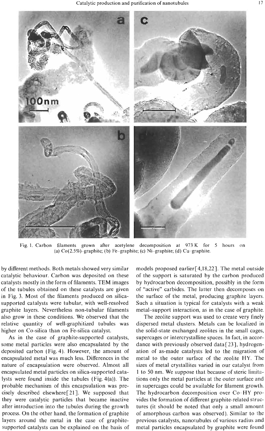
The structure of the filaments was
different
on
the various metals. We have observed
the formation of hollow structures
on
the surface
of
Co and Fe catalysts.
On
Cu
and
Ni,
carbon was
deposited in the form
of
irregular fibres. The detailed
observation showed fragments
of
turbostratic graph-
ite sheets
on
the latter catalysts. The tubular filaments
on
Fe- and Co-graphite sometimes possessed well-
crystalline graphite layers.
In
the same growth batch
we also observed a large amount of non-hollow
filaments with a structure similar to that observed
on
Cu
and Ni catalysts.
In
general, encapsulated metal particles were
observed
.
on
all graphite-supported catalysts.
According to Ref.
[4]
it can be the result of a rather
weak metal-graphite interaction. We mention the
existence
of
two types of encapsulated metal particles:
those enclosed in filaments (Fig.
1)
and those encap-
sulated by graphite. It
is
interesting to note that
graphite layers were parallel to the surface of the
encapsulated particles.
As was found in Ref.
[
131,
the method of catalytic
decomposition
of
acetylene
on
graphite-supported
catalysts provides the formation of very long
(50
pm)
tubes. We also observed the formation
of
filaments
up to 60pm length
on
Fe-
and
Co-graphite.
In
all
cases these long tubules were rather thick. The thick-
ness
varied from
40
to
100
nm.
Note that the disper-
sion of metal particles varied in the same range. Some
metal aggregates of around
500
nm
in diameter were
also found after the procedure
of
catalyst pretreat-
ment (Fig.
2).
Only a very small amount of thin
(20-40
nm
diameter) tubules was observed.
The as-produced filaments were very strongly
covered by amorphous carbon produced by thermal
pyrolysis of acetylene. The amount of amorphous
carbon varied with the reaction conditions. It
increased with increasing reaction temperature and
with the percentage of acetylene in the reaction
mixture. Even in optimal conditions not less than
50%
of the carbon was deposited in the form of
amorphous carbon in accordance with[
131.
As
it was established by Geus
et
aL[l8,
191
the
decrease of the rate
of
carbon deposition is a positive
factor for the growth
of
fibres
on
metal catalysts.
SiO, is an inhibitor
of
carbon condensation as was
shown in Ref.
[20].
This support also provides possi-
bilities for the stabilization of metal dispersion. Co
and Fe, i.e. the metals that give the best results for
the tubular condensation of carbon
on
graphite
support, were introduced
on
the surface of silica gel
Table
1.
Method
of
preparation
and
metal content
of
the catalysts
Metal particle
Poae
0
Method
of
Metal diameteP
Sample
(A)
preparation (wt%) (nm)
Co-graphite
F-phite
Ni-graphite
-aphite
Co-SiO,
Co-Si0,-1
Co-Si02-2
Fe-SiO,
CO-HY
-
-
-
-
90
7.5
40
90
90
Impregnation
0.5-10
Impregnation 2.5
Impregnation 2.5
Impregnation 2.5
Ion exchange precipitation 2.1
Solid state ion exchange
8
Pore impregnation 2.5
Pore impregnation 2.5
Pore impregnation 2.5
1Cb100
2
100
2
loo
2
loo
2-2Ob
1-50
10-100
10-100
10-100
"Measured by SEM
and
TEM.
%e distribution
of
the
particles
was
also
measured (Fig. 6).
Catalytic production and purification
of
nanotubules
17
Fig.
1.
Carbon filaments grown after acetylene decomposition at
973
K
for
5
hours on
(a) Co(2.5%)-graphite;
(b)
Fe-graphite; (c) Ni-graphite; (d) Cu-graphite.
by different methods. Both metals showed very similar
catalytic behaviour. Carbon was deposited on these
catalysts mostly in the form of filaments. TEM images
of the tubules obtained on these catalysts are given
in Fig. 3. Most of the filaments produced on silica-
supported catalysts were tubular, with well-resolved
graphite layers. Nevertheless non-tubular filaments
also grow in these conditions. We observed that the
relative quantity of well-graphitized tubules was
higher on Co-silica than on Fe-silica catalyst.
As in the case of graphite-supported catalysts,
some metal particles were also encapsulated by the
deposited carbon (Fig. 4). However, the amount of
encapsulated metal was much less. Differences in the
nature of encapsulation were observed. Almost all
encapsulated metal particles on silica-supported cata-
lysts were found inside the tubules (Fig. 4(a)). The
probable mechanism of this encapsulation was pre-
cisely described elsewhere[ 213. We supposed that
they were catalytic particles that became inactive
after introduction into the tubules during the growth
process. On the other hand, the formation of graphite
layers around the metal in the case of graphite-
supported catalysts can be explained on the basis of
models proposed earlier[4,18,22]. The metal outside
of the support is saturated by the carbon produced
by hydrocarbon decomposition, possibly in the form
of “active” carbides. The latter then decomposes on
the surface
of
the metal, producing graphite layers.
Such a situation is typical for catalysts with a weak
metal-support interaction, as in the case of graphite.
The zeolite support was used to create very finely
dispersed metal clusters. Metals can be localized in
the solid-state exchanged zeolites in the small cages,
supercages or intercrystalline spaces. In fact, in accor-
dance with previously observed data
[
231, hydrogen-
ation of as-made catalysts led to the migration
of
metal to the outer surface of the zeolite HY. The
sizes
of
metal crystallites varied in our catalyst from
1
to
50
nm. We suppose that because of steric limita-
tions only the metal particles at the outer surface and
in supercages could be available for filament growth.
The hydrocarbon decomposition over Co-HY pro-
vides the formation
of
different graphite-related struc-
tures (it should be noted that only a small amount
of
amorphous carbon was observed). Similar to the
previous catalysts, nanotubules of various radius and
metal particles encapsulated by graphite were found