Buschow K.H.J. (Ed.) Concise Encyclopedia of Magnetic and Superconducting Materials
Подождите немного. Документ загружается.


resolution of 13 eV FWHM at 6 keV and a spatial
resolution of 0.5 mmina20mm length has been ob-
tained with an epitaxial tantalum strip detector with
STJs at each end. The detector response time is lim-
ited by the diffusion of quasiparticles in the epitaxial
film, and the lifetime of the quasiparticles trapped
near the STJs. The count rate capability of these im-
aging strips is typically less than 1000 counts per sec-
ond. Similar systems have also been shown to work
with optical photons.
3. Hybrid Detectors
Microcalorimeters and STJ detectors have been com-
bined in several interesting ways. One example is the
aluminum STJ described above with a lead absorber.
In some WIMP detectors, pads of aluminum are de-
posited on semiconducting crystals. Each aluminum
pad is coupled to a TES. When a photon or particle is
absorbed in the crystal, nonequilibrium phonons are
generated as well as electron–hole pairs. The phonons
are absorbed in the aluminum pads where they break
Cooper pairs creating excess quasiparticles. These
quasiparticles then diffuse in the aluminum and col-
lect in the TES. The quasiparticles heat the TES,
creating a current pulse in the amplifier.
Another interesting hybrid detector is the normal
metal-insulator-superconductor (NIS) tunnel junc-
tion microcalorimeter. In this detector the photon or
particle heats the electrons in the normal-metal film.
This heating causes more electrons to tunnel through
the insulating barrier into the superconductor. This
current pulse is measured using a SQUID current
amplifier. While the NIS tunnel junction uses tunnel-
ing, it is the temperature rise of the electrons in the
normal metal that determines its ultimate perform-
ance. The resolution is thus limited by the microcal-
orimeter Eqn. (2) with xB1.3. The best energy
resolution obtained with an NIS tunnel junction mi-
crocalorimeter is 22 eV FWHM at 6 keV.
An interesting feature of the NIS tunnel junction is
that the tunneling of hot electrons out of the normal
metal is a cooling process. If the energy of these
electrons can be removed from the system, the tem-
perature of the normal metal can be lowered below
the bath temperature. This property has been ex-
ploited to build microrefrigerators from NIS tunnel
junctions. These microrefrigerators may be useful for
cooling detectors or other small low-power devices
from 0.3 K to 0.1 K, or from 0.1 K to as low 20 mK.
4. Superconducting Granules
A superheated superconducting granule (SSG) parti-
cle detector consists of small type-one supercon-
ducting spheres suspended in a dielectric. The spheres
are cooled below their transition temperature, and
then a magnetic field is applied. The magnetic field is
adjusted to a value just below the field required to
drive the spheres into their normal state. In this con-
figuration, a small temperature increase within a
sphere will cause the sphere to undergo a sudden
phase transition to the normal state. When a sphere is
in the superconducting state, the magnetic field is
screened from its interior by the Meissner effect.
During the phase transition to the normal state, the
magnetic field penetrates the sphere. This results in a
sudden change in magnetic flux, which can be meas-
ured by coils surrounding the spheres. Small (30 mm
in diameter) spheres of tin or zinc are typically used.
At 0.1 K, the heat capacity of these spheres is small
enough that only a few electron volts of energy are
needed to produce a phase transition.
Unlike microcalorimeters which measure the total
energy deposited, SSGs measure only that the energy
deposited was above a certain threshold. Some energy
information from a constant source can be obtained
by scanning the magnetic field. The sensitivity of the
SSG particle detector is limited by variations from
sphere to sphere in the energy required to produce a
phase transition. Various fabrication techniques have
been developed which provide a threshold accuracy
of about 2%. With this accuracy, it is possible to
distinguish between ionizing particles that induce
several spheres to undergo phase transitions, and nu-
clear recoils that excite only one sphere. Detectors
with billions of spheres are used for WIMP-search
experiments.
See also: SQUIDs: The Instrument; SQUIDs:
Amplifiers
Bibliography
Booth N E, Cabrera B, Fiorini E 1996 Low-temperature particle
detectors. Annu. Rev. Nucl. Part. Sci. 46, 471–532
de Korte P, Peacock T (eds.) 2000 Proceedings of the 8th
International Workshop on Low-temperature Detectors
(LTD-8). Nucl. Instrum. Methods A. 444
Frank M, Hiller L J, le Grand J B, Mears C A, Labov S E,
Lindeman M A, Netel H, Chow D, Barfknecht A T 1998
Energy resolution and high count rate performance of su-
perconducting tunnel junction x-ray spectrometers. Rev. Sci.
Instrum. 69, 25–31
Kraus H 1996 Superconductive bolometers and calorimeters.
Supercond. Sci. Technol. 9, 827–42
Moseley S H, Mather J C, McCammon D 1984 Thermal de-
tectors as x-ray spectrometers. J. Appl. Phys. 56, 1257–62
Pretzl K 2000 Cryogenic calorimeters in astro and particle
physics. Nucl. Instrum. Methods A 454, 114–27
Wollman D A, Irwin K D, Hilton G C, Dulcie L L, Newbury D
E, Martinis J M 1997 High-resolution, energy-dispersive
microcalorimeter spectrometer for x-ray microanalysis. J.
Microsc. 188, 196–223
S. E. Labov and J. N. Ullom
Lawrence Livermore National Laboratory, Livermore
California, USA
1070
Radiation and Particle Detectors
Random Access Memories: Magnetic
A variety of magnetic random access memory
(MRAM) technologies have been explored over a
period of many decades. Their advantages include an
unlimited number of read-write cycles, random access
to any address, radiation hardness, and nonvolatility
(namely, the state of the memory does not require
periodic refreshing and is maintained even when
power is removed from the memory).
MRAM was originally in use for 30–40 years as
magnetic core memory, which was then the only af-
fordable RAM, although very labor-intensive and
having a high cost per bit, before the advent of static
RAM (SRAM) and dynamic RAM (DRAM) in the
form of integrated circuits. It should be noted that
while core memory has disappeared from most com-
puters, there are still a number of applications for it
in specialized systems, primarily military and space
systems. Early interest, centered on magnetic bubble
technology, was not successful, and involved an up-
per layer of permalloy patterned into a T-I bar struc-
ture and a lower layer of a garnet material with a
single anisotropy direction perpendicular to the sur-
face. Magnetic thin films were considered as an al-
ternative to core memory. Since about the early
1990s, there has been a renewed interest in MRAMs
by replacing thin film with anisotropic magnetoresis-
tive (MR) bit structures. However, these nonvolatile
memory technologies are of comparatively poor per-
formance and thus limited in their applications. The
small number of suppliers would be a concern for
systems requiring long-term maintenance or likely
upgrade (Jorgensen 1979, Daughton 1992).
The demand for nonvolatile radiation-hard mem-
ory has continued with additional pressures for high-
er density, lower power, higher speeds, and lower cost
per bit. The present efforts to develop mainly three
different versions of nonvolatile solid-state memories
are a response to this. First, an MRAM using the
spin-valve (SV) effect has been shown to have a fast
switching signal (see Magnetic Recording Systems:
Spin Valves). Second, an erasable programmable
read-only memory (EPROM) employing the Hall ef-
fect to detect the fringe field of a ferromagnetic stor-
age element has also been proposed. The third
development underway is so-called spin-dependent
tunneling (SDT) MRAM. This article reviews pro-
gress in MRAMs and outlines the prospects for fu-
ture developments.
1. MRAM Using the Spin-valve Effect
MRAM using the spin-valve (SV) effect is evolved
from that using the MR effect. A spin-valve is com-
posed of two ferromagnetic (FM) layers (such as
Permalloy or cobalt) with a spacer layer of a non-
magnetic conductor (typically copper). In principle,
in the sandwich structures exhibiting the SV effect the
resistance is lower when alternate magnetizations are
parallel than when they are antiparallel (Daughton
and Chen 1993, Matsuyama et al. 1997). The access
time of the MRAM depends on sense signal, and
currently this is limited by the 2% MR thin-film ma-
terials used today. The improvement in sensing time
with larger signals is roughly equal to the square of
improvement in signal. This is because, for a given
signal-to-noise ratio (SNR), the sense system band-
width may be increased by the square of the sense
signal improvement. A 10-fold improvement in signal
is possible with SV materials, and this would improve
read access times of the densest MRAMs to about the
same level as DRAMs (Daughton 1992).
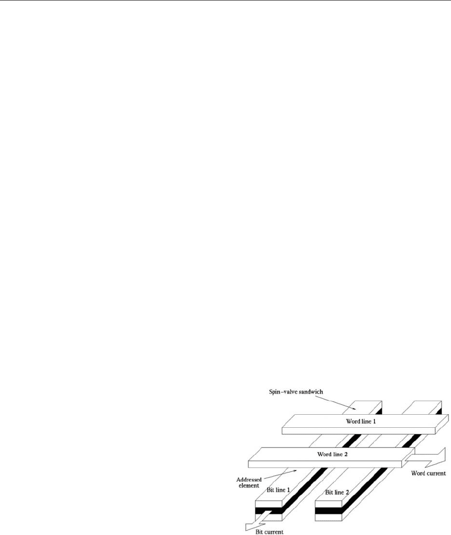
Figure 1 is an MRAM architecture using the
FM(hard)–conductor–FM(soft) SV sandwich pro-
posed by Wang and coworkers in 1995 (Wang and
Nakamura 1995a). This memory requires SV bit lines
and word lines. In an SV sandwich there are two
kinds of ferromagnetic layers, which possess different
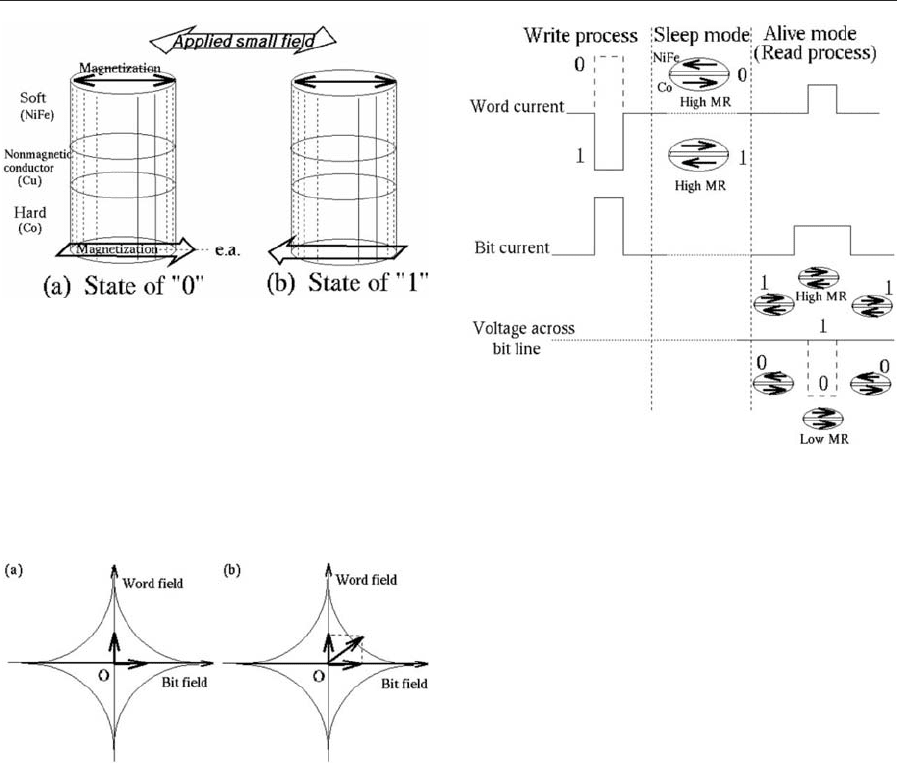
coercivities. As shown in Fig. 2, this memory operates
on the general principle of storing a binary datum in
the magnetically hard layer (cobalt) and sensing its
remanent state by switching the magnetically soft
layer (NiFe) in such a way that the magnetic state of
the hard layer remains unaltered. The parallel and
antiparallel states between magnetizations will give a
different readout.
Addressing any desired element in a two-dimen-
sional array is a basic requirement for MRAMs. This
is realized by means of the ‘‘astroid-shaped’’ switching
characteristics of a uniaxial anisotropic ferromagnetic
thin film. As depicted in Fig. 3, the switching field in
the longitudinal direction is lowered when a trans-
verse field is applied. The word lines and bit lines,
Figure 1
SV-MRAM architecture using SV sandwich. The word
lines and SV bit lines, which are orthogonal to each
other, are used for selection purposes. The shorting bars
between elements to reduce the bit line resistance are not
shown in this figure.
1071
Random Access Memories: Magnetic
which are orthogonal to each other, are used for se-
lection purpose (see Fig. 1). A word current passes
through one of the word lines and a bit current
through one of the bit lines. The bit current is as-
sumed to flow mainly along the intermediate layer
(e.g., copper) of the SV sandwich owing to its large
conductivity. These two currents combine at one and
only one intersection point, i.e., the addressed ele-
ment. As depicted in Fig. 3(a), neither the word field
(current) with selected value nor the bit field (current)
with selected value is by itself able to switch the
element. In Fig. 3(b), if both fields act together, they
are able to produce a combined field vector greater
than the switching threshold of the addressed element.
In such a way, a writing or re-writing operation is
realized (Wang and Nakamura 1996a).
Magnetization configuration of an SV-MRAM
element and its expected writing and reading timing
diagram is shown in Fig. 4. During a write operation,
the sign of the word current will define the stored bit
value, ‘‘0’’ or ‘‘1.’’ In the absence of external field
(sleep mode), the alternate magnetizations are anti-
parallel, owing to the interlayer antiferromagnetic
coupling, giving small self-demagnetizing fields and
small external stray fields on nearby memory ele-
ments, both of which could help with element stabil-
ity. During a read operation (alive mode), data
readout is performed by monitoring the voltage
response of the SV bit line against a positive word
current, whose value is not sufficient to switch the
hard layer, but switches the soft layer if it opposes
the soft layer’s magnetization. A different voltage,
depending on whether a ‘‘0’’ or ‘‘1’’ is stored, should
appear across that SV bit line. In the experimental
pulse sequence (Wang and Nakamura 1995a), the
sense current applied into the bit line is 5 mA and
a sense output voltage of 8 mV appears. The read/
write energy is quite low. Furthermore, the test in-
dicates that a stable readout state involving 3 10
8
repeated reversals, by field cycling, of the soft layer’s
Figure 3
How to address a desired element in a two-dimensional
array with the aid of astroid-shaped switching
characteristics? (a) Neither the word field (with selected
value) nor the bit field (with selected value) by
themselves are able to switch the element; (b) both fields
act together to produce a combined field vector greater
than the switching threshold of the addressed element.
Figure 4
Magnetization configuration of an SV-MRAM element
and its expected writing and reading timing diagram. In
the absence of external field (sleep mode), the alternate
magnetizations are antiparallel due to the inter-layer
antiferromagnetic coupling.
Figure 2
Schematic drawing of SV-MRAM. This memory
operates on the general principle of storing binary
datum in the magnetically hard layer (e.g., Co) and
sensing its remanent state by switching the magnetically
soft layer (e.g., NiFe) in such a way that the magnetic
state of the hard layer remains unaltered (after Wang
and Nakamura 1995a). The parallel and antiparallel
states between magnetizations will give a different
readout (spin-valve effect).
1072
Random Access Memories: Magnetic
magnetization is achieved, without gradual decay and
eventual erasure of the hard layer’s magnetization.
Thus this SV-MRAM is confirmed to have a non-
destructive readout (NDRO) property.
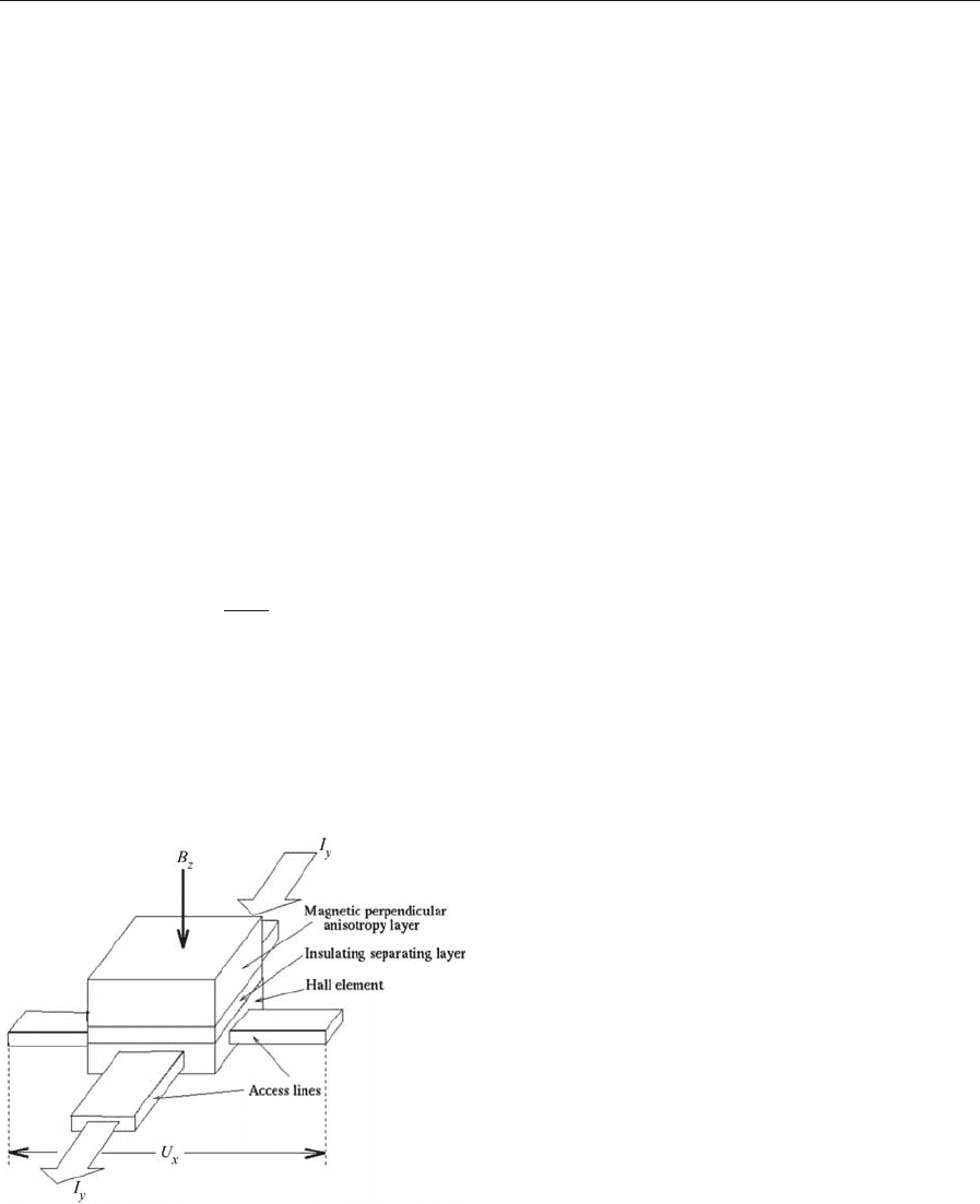
2. EPROM Using Hall Effect
An erasable programmable read-only memory
(EPROM) using the Hall effect to detect the direc-
tion of magnetic moment of a ferromagnetic storage
element has been proposed by Timoshkov et al ., as
shown in Fig. 5 (Timoshkov et al. 1996). The mag-
netic film of high coercivity and perpendicular an-
isotropy is used for data storage, and the Hall
element for data reading. The insulating layer be-
tween them produces electrical isolation of the func-
tional layers. The data recording process is realized
by magnetizing the perpendicular anisotropy layer.
The magnetic flux B
Z
of this layer penetrates through
the Hall element, and the data read process is carried
out by the Hall effect in the semiconductor material.
The read time for such a memory is limited only by
the relaxation time of the Hall effect processes and is
equal to 10
12
–10
13
second. The equation for the
Hall voltage U
X
is
U
X
¼ r
H
I
Y
B
Z
ned
f ðl=aÞð1Þ
where r
H
is the Hall factor depending on prevalent
scattering mechanism of the carriers, 1.18–1.93; I
Y
is
the sense current; e is unit electric charge, 1.6 10
19
C; n and d are the carrier concentration in the semi-
conductor (data reading) layer and its width respec-
tively; and f(l/a) is a correction function, which is
equal to 0.90–0.95 for a reasonable ratio of the length
to the width of the data reading layer l/a ¼23.
3. MRAM Using Spin-dependent Tunneling
(SDT) Effect
The SDT effect (Julliere 1975, Miyazaki and Tezuka
1995, Moodera et al. 1995, Boeck 1998) is a special
current-perpendicular-to-plane (CPP) giant magneto-
resistance (GMR) effect, based on FM–tunnel–barri-
er–FM spin-polarized junctions. The tunneling
resistance between two ferromagnetic metal layers
that are separated by a thin insulator depends on the
relative orientation of the magnetization of each layer.
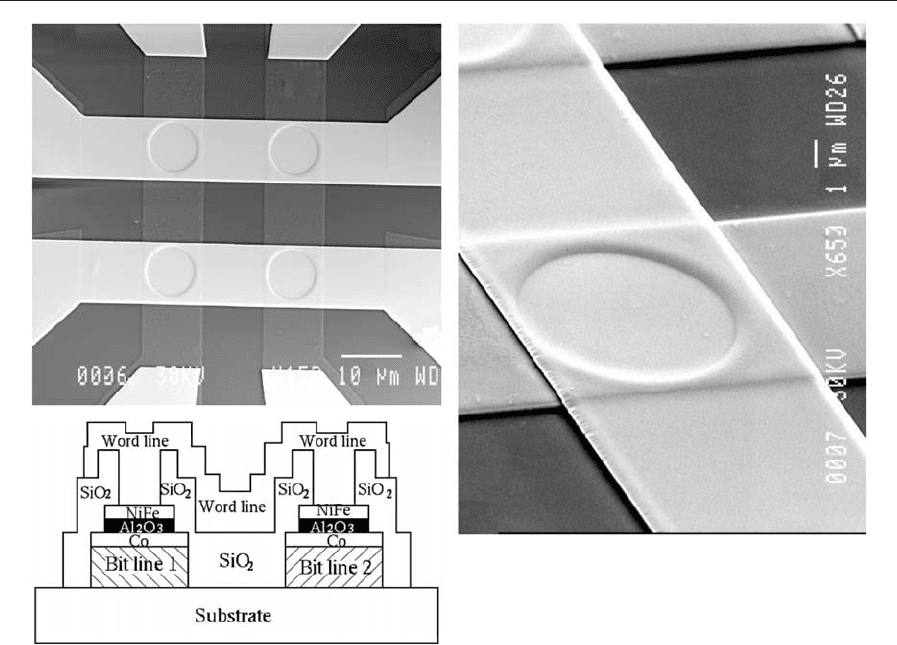
Work by Wang et al. on the MRAM using the
SDT effect began in 1994 (Wang and Nakamura
1995b, 1996b), and led initially to the successful fab-
rication of a 2 2 bit SDT-MRAM, based on Co/
Al
2
O
3
/80NiFe tunnel junctions. Figure 6 is its scan-
ning electron microscopy (SEM) picture and sche-
matic. The chiplet has eight contact pads, which
provides the required flexibility in connecting the test
site to the peripheral select/drive circuitry. The spin-
tunneling junction dimensions varied between 2 and
50 mm. All the spin tunneling samples Co(100 nm)/
Al
2
O
3
(3–8 nm)/80NiFe(100 nm) were prepared by ra-
dio frequency (rf) sputtering with argon. The inter-
mediate Al
2
O
3
was formed by oxidation in the
atmosphere. Uniaxial magneto-crystalline anisotropy
in ferromagnetic films, important both for memory
storage and for the way that a bit is selected, was
induced by a magnetic field applied during sputtering.
Contact windows were opened in the insulator to al-
low the orthogonal top leads and bottom leads to
access the junctions directly. The top leads are visible
as brighter regions in the SEM picture, whereas the
bottom leads are darker.
As shown in Fig. 7, the structure of the SDT-
MRAM is relatively simple, compared with the semi-
conductor memories. Having an active memory-cell
transistor, flash EEPROMs (electrically erasable pro-
grammable ROMs) typify semiconductor memories.
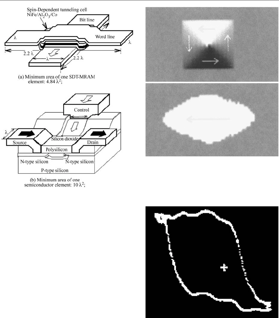
The minimum element area of a tunneling cell is 4.84
l
2
, where l is the resolution limit of the lithography
used to fabricate the memory elements. Progress in
photolithography technology should enable the re-
duction of l beyond the 200 nm limit (Daughton
1992). Compared with the minimum size of a
memory-element transistor, over 10l
2
(also shown
in Fig. 7), the SDT-MRAM can potentially be at
least twice as dense.
The spin-tunneling junction was designed with a
circular shape to benefit the formation of single-do-
main structure, based on the micromagnetic simula-
tion result (He and Wang 1999), as shown in Fig. 8.
For each MRAM element there should exist only
two possible states of magnetization, e.g., left and
right. Clearly this is the case for an elliptic or circular
Figure 5
An EPROM using the Hall effect to detect the direction
of magnetic moment of a ferromagnetic perpendicular
storage element (after Timoshkov et al . 1996).
1073
Random Access Memories: Magnetic
island. In detail, for a single domain island one can be
sure that the island switches completely in a proper
writing process. A multi-domain state found in the
square patterned island would lead to a miscellaneous
logic in a one bit per island recording system. This is
because more than two states are possible and the
island might not have switched completely after writ-
ing. As a consequence, the magnetization of the is-
land becomes unstable and the result of a next writing
process may be unpredictable.
An isolated memory element was tested. Figure 9
illustrates the R(H) response’s minor loops operating
in the mode in which only the magnetically soft layer
is switched by applying a field of 71.6 kA m
1
and
the sample is initially saturated by þ3.2 kA m
1
.
Note that the MR hysteresis at zero field represents
different magnetization combinations, thereby yield-
ing different resistance values.
The on-chip parallel write/read operations were
successfully performed. Writing the information
involves a switching of the soft layer’s magnetiza-
tion, ideally without affecting the reference (hard)
layer’s magnetization. (In a memory device, inde-
pendent switching of the magnetically soft layer is
achieved by making the other layer either magneti-
cally hard or exchange-biased by an antiferromag-
netic layer, e.g., MnFe.) Reading the information
only requires a measurement of magnetoresistance.
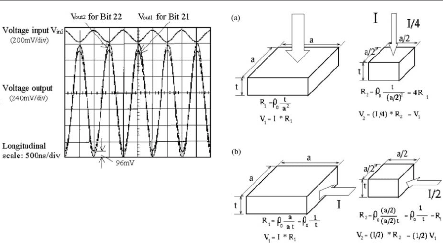
An output voltage change of 96 mV, as shown in
Fig. 10, between the binary bit states against a
sine-wave sense voltage of 160 mV, 1 MHz has been
observed. This is a reproducible readout state.
Ultra-dense magnetic solid-state MRAMs will
probably be limited by the minimum signal level.
As a comparison, we first deduce the signal level in
conventional current-in-plane (CIP)-type MR or SV
MRAM. Its signal is given by
Signal
CIP
¼ fJ
max
lDr ð2Þ
Figure 6
SEM micrographs of a 2 2 bit SDT-MRAM chiplet showing the test site containing 8 contact pads and 4 circular
tunnel junctions, each 10 mm in diameter, the schematic cross-section (note the CPP structure) and a single-tunnel
junction bit. The top leads are visible as bright regions in SEM whereas the orthogonal bottom leads are darker (after
Wang and Nakamura 1996b).
1074
Random Access Memories: Magnetic
where f is a factor smaller than one which depends
on the mode of storing and sensing information, J
max
is the maximum current per cross-sectional area
allowed by thermal dissipation, and Dr is the change
of resistivity. Thus at the maximum current density,
the signal level is proportional to the element size l.
As the storage density increases, the signal level
will decrease. In contrast, the signal of SDT-MRAM
results in
Signal
CPP
¼ fJ
max
tDr ð3Þ
where t is the total thickness of the spin-tunneling
junction. As illustrated in Fig. 11, at a maximum
sense current density, the signal level of SDT-MRAM
is obviously independent of its cross-sectional area l
2
.
This result is so attractive that the density of SDT-
MRAM should not be limited by signal degradation.
It is suggested that density-independent signal level is
Figure 7
Structure comparison of the SDT-MRAM and the
semiconductor memory. In (b) a field effect transistor
(FET) comprises a source and a drain contact to send
current through a semiconductor channel and a gate
control to modulate the carrier density in the channel.
Here l is the resolution limit of the lithography used to
fabricate the memory elements.
Figure 8
Demagnetized states of patterned islands with different
shapes. The brightness stands for the left magnetization
direction and the darkness for the right (after He and
Wang 1999).
Figure 9
Measured resistance versus applied field R(H) for
Co/Al
2
O
3
/80NiFe. The applied field is limited at
71.6 kA m
1
and the sample is initially saturated by
þ3.2 kA m
1
. Note that the MR hysteresis at zero field
represents different magnetization combinations thereby
yielding different magnetoresistances (after Wang and
Nakamura 1995b).
1075
Random Access Memories: Magnetic
the biggest advantage of CPP-type SDT-MRAM,
compared with CIP-type MR or SV MRAM.
It is pointed out that the SDT-MRAM’s signal re-
mains constant while the CIP MRAM’s signal drops
with increasing density. However, the Johnson noise
with SDT-MRAM may become a limiting factor in
scaling the MRAM element to submicron sizes be-
cause this component of noise becomes increasingly
important and may even dominate the total noise.
What matters for practical application is SNR. Even
the larger signals available from SV structures do not
make SV-MRAM attractive for mainstream RAM
applications. In order to achieve reasonable memory
array densities many SV elements (of number n) have
to be electrically connected in series, which means
that the actual signal available when reading one
particular element is MR/n (see Fig. 1 for reference).
Thus, a severe practical problem is encountered that
ultra-dense CIP SV-MRAM will be limited by low
SNR. By contrast, as illustrated in Fig. 6, the high
MR signal from the individual junction element can
be fully utilized in a cross-point architecture by con-
necting each element in parallel. In this case, the SNR
in an n bit n bit SDT-MRAM is independent of n,
which is normally a big number. As a result, although
SNR in both CIP and CPP MRAMs falls with in-
creasing density, the SNR for the CPP SDT-MRAM
remains much larger than for the CIP type MR or
SVMRAM.
So far, the experimental results of SDT-MRAM
are only for a low-density case in that only 2 2 bit
elements are included. For a dense or ultra-dense
MRAM, the cross-talk from an addressed element to
adjacent elements may cause mis-selection and creep
problems (after many such disturbances the magnetic
state of these bits creeps either to some intermediate
state or may completely reverse). Note also that the
driving field required to switch the layer increases as a
result of the decreased length of the element, owing to
the demagnetization effect. To address these issues, a
finite element method (FEM) was used to study the
electromagnetic behavior of SDT-MRAM (Wang
et al. 1997). Three keepered SDT-MRAM designs
have been considered, as shown in Fig. 12. A low-cost
conventional keeperless MRAM design (Fig. 12(a)) is
taken as our reference. To localize the field, an im-
proved partially keepered MRAM design (Fig. 12(b))
differs from the reference MRAM by the addition of
partial keepers, with high permeability, above the bit
lines and underneath the word lines. The third design,
known as the continuously keepered MRAM design,
is shown in Fig. 12(c). In this design, additional con-
tinuous keepers with 0.1 mm thickness are formed. It
was hypothesized that the drive field would be con-
fined within the nearly closed keeper, effectively en-
hancing the driving field and reducing interference
between adjacent cells. The continuously keepered
MRAM design was found to reduce the cross-talk by
a factor of five and reduce the driving current by a
factor of four, compared with a conventional keep-
erless design, which will be the most favored ap-
proach for achieving 10
9
bits cm
2
areal density.
Figure 10
Reproducible read waveform. An output voltage change
of 96 mV (after an amplifier) between the binary bit
states against a sine-wave voltage excitation (the above)
of 160 mV, 1 MHz has been observed. The vertical scale
is 1.2 V/div and the horizontal scale is 500 ns/div.
Figure 11
Halving the dimension of an MRAM cell will cause
different results on signal amplitude. In the CPP design
of (a), signal remains; in the CIP design of (b), signal
drops by a factor of 2. Note that both (a) and (b) are at a
maximum sense current density.
1076
Random Access Memories: Magnetic
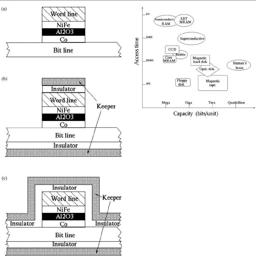
4. Conclusions
Read-access time and storage density are the twin
keys to computer data storage devices. Although new
electronic devices, processor organizations and soft-
ware systems have contributed to enormous advances
in computer technology, they would have been
worthless without the faster and denser memories
that were developed with them. The SDT-MRAM
outlined here, the most promising candidate for mag-
netic nonvolatile memory, is likely to achieve very
high densities. From Fig. 13 it can be seen that SDT-
MRAM, which is simply structured, may in some
applications potentially exhibit excellent properties
superior to semiconductor memories and/or magnetic
disks. In particular, the density-independent signal
level is the biggest advantage of CPP-type SDT-
MRAM, compared with the conventional CIP-type
MR or SV MRAM, whose signal level is inversely
proportional to the square root of the storage den-
sity. Furthermore, it has also been demonstrated that
although the Johnson noise makes a large contribu-
tion to the total noise, it does not significantly de-
grade the performance of the device, because the
SNR for the SDT-MRAM remains much larger than
for the CIP MR or SV MRAM even at high storage
density.
Another important parameter for SDT-MRAM is
the intrinsic RC time constant of the device. Because
of the insulator between electrodes, junctions also act
as a parallel plate capacitor. The reason that the RC
time constant is important for memory application is
because of speed limitations in reading data from a
memory element. The RC time constant is independ-
ent of the area of the junction and exponentially
dependent on the thickness of the barrier and can
be reduced until the processing difficulties with
thin barriers prevent further reduction in thickness.
For modern MRAM applications, the equivalent
Figure 12
Three keepered SDT-MRAM designs: (a) conventional
keeper-less MRAM design; (b) improved partially
keepered MRAM design; (c) further improved
continuously keepered MRAM design (after Wang et al.
1997).
Figure 13
The position of SDT-MRAM in various data storage
devices.
1077
Random Access Memories: Magnetic

resistance for SDT devices must be at the lower end
of the resistance range. Parkin et al. found that the
resistance-area products of magnetic tunnel junctions
can be varied from 10
9
Omm
2
to as low as 60 Omm
2
by
varying the aluminum thickness and properly oxidiz-
ing it (Parkin et al. 1999). Incomplete oxidation leads
to the presence of metallic aluminum in the barrier,
which results in a rapid suppression of the tunnel
junction magnetoresistance. Based on these facts, the
RC time constant for the junctions should be of the
order of nanoseconds (Wong et al. 1998, Sousa et al.
1999). Nevertheless, such a SDT-MRAM has to be
read with a silicon sense amplifier. This means a
mixed silicon-tunneling structure: the X-Y decoders/
sense amplifiers in an array in silicon with ‘‘holes’’ to
be filled in by tunneling array. Thus, the speed of the
device will probably be limited by silicon technology.
(Today, the speed of experimental silicon devices has
improved to 1 ns and will be expected to dip below
this in future.) There is no significant access-time ad-
vantage for the tunneling design as compared to the
bipolar devices.
As well as the continuing developments which are
always to be expected in semiconductor memory
technology, it is also interesting to note other novel
technologies, such as the spin-dependent tunneling
(SDT) effect. In the immediate future DRAM will
continue as the densest semiconductor memory, but
MRAM using the SDT effect looks set to take the
lead in the medium and longer term and is a very
important development for applications where non-
volatility, higher density, radiation hardness and low-
er power are required. Prototypes are out, technology
is maturing, and the advances mentioned in this ar-
ticle would speed up the pace of the application of
MRAM, since a microstructured junction might serve
as a high-capacity and low-power substitute for con-
ventional semi-conductor memories.
Bibliography
Boeck J D 1998 Switching with hot spins. Science 281, 357–9
Daughton J M 1992 Magnetoresistive memory technology.
Thin Solid Films 162–216
Daughton J M, Chen Y J 1993 GMR materials for low field
applications. IEEE Trans. Magn. 29 (6), 2705–10
He L, Wang F Z 1999 Size and shape effects of patterned po-
lycrystalline islands. Intermag HC-09
Jorgensen F 1979 The Complete Handbook of Magnetic Re-
cording. Blue Ridge, Summit, PA
Julliere M 1975 Tunneling between ferromagnetic films. Phys.
Lett. A 54, 225–6
Matsuyama K, Asada H, Ikeda K, Taniguchi K 1997 Low
current magnetic-RAM memory operation with a high sen-
sitive spin valve material. IEEE Trans. Magn. 33 (5), 3283–5
Miyazaki T, Tezuka N 1995 Giant magnetic tunneling effect in
a Fe/Al
2
O
3
/Fe junction. J. Magn. Magn. Mater. L231–4, 139
Moodera J S, Kinder L R, Wong T M, Meservey R 1995 Large
magnetoresistance at room temperature in ferromagnetic thin
film tunnel junctions. Phys. Rev. Lett. 74 (16), 3273–6
Parkin S S, Roche K P, Samant M G, Rice P M, Beyers R B,
Scheueriein, O’Sullivan E J, Brown S L, Bucchigano J,
Abraham D W, Lu Y, Rooks M, Trouilloud P L, Wanner
R A Gallagher W J 1999 Exchange-biased magnetic tunnel
junctions and application to nonvolatile magnetic random
access memory. J. Appl. Phys. 85(8)
Sousa R C, Freitas P P, Chu V, Conde J 1999 Vertical inte-
gration of a spin dependent tunnel junction with an amor-
phous Si diode for MRAM applications. Intermag HA-03
Timoshkov Y, Khomenok V Danko V Kurmashev V 1996 The
memory element. Russ. Fed. Pat. N.2036517
Wang F Z, Mapps D, He L, Clegg W W, Nakamura Y 1997
Feasibility of ultra-dense spin-tunneling random access mem-
ory (STram). IEEE Trans. Magn. 33 (6), 4498–512
Wang F Z, Nakamura Y 1995a A new type of memory using
GMR effect. IEICE Gen. Conf. Proc. C-502. Fukuoka, Japan
Wang F Z, Nakamura Y 1995b Perpendicular GMR random
access memory using magnetic tunneling effect. J. Magn. Soc.
Jpn. 19 (S2), 108–11
Wang F Z, Nakamura Y 1996a Design, simulation, and real-
ization of solid state memory element using the weakly cou-
pled GMR effect. IEEE Trans. Magn. 32 (2), 520–6
Wang F Z, Nakamura Y 1996b Spin tunneling random access
memory (STram). IEEE Trans. Magn. 32 (5), 4022–4
Wong P K, Evetts J E, Blamire G 1998 High conductance small
area magnetoresistive tunnel junctions. Appl. Phys. Lett. 73
(3), 384–6
F. Z. Wang
University of North London, UK
Rare Earth Intermetallics: Thermopower of
Cerium, Samarium, and Europium
Compounds
The thermoelectric power, S, is known as a transport
property that is very sensitive to details of the elec-
tronic structure at the Fermi energy. Cerium com-
pounds exhibit widely different types of anomalous
physical properties owing to the hybridization of ce-
rium 4f electrons and conduction electrons. There is
already an accumulation of experimental data for S
for a large number of cerium compounds; however,
there has been no review article concerning these
data, as far as is known. The aim of this article is to
give an overview and discussion of these data for S
for different types of cerium compounds.
This article is based on previous review papers by
Sakurai (1993), and Sakurai et al. (1996). Anomalous
physical properties of cerium compounds are of in-
terest with respect to highly correlated electron sys-
tems (see Electron Systems: Strong Correlations).
Doniach (1977) considered a competition of two in-
teractions: the Kondo interaction between the cerium
4f electrons and the conduction electrons (character-
istic temperature T
K
) and the RKKY interaction be-
tween the 4f electrons on different lattice sites via the
conduction electrons (characteristic temperature T
N
1078
Rare Earth Intermetallics: Thermopower of Cerium, Samarium, and Europium Compounds
for an antiferromagnet or T
C
for a ferromagnet). The
former interaction causes the cerium 4f electrons and
the conduction electrons to form a hybridized non-
magnetic singlet state for temperatures ToT
K
, but
the cerium 4f electrons regain their magnetic moment
for T4T
K
. The latter interaction gives rise to an an-
tiferromagnetic state of the cerium 4f electrons for
ToT
N
(or a ferromagnetic state for ToT
C
) and to a
paramagnetic state with a random orientation of the
magnetic moments for T
N
(or T
C
)oT.
These characteristic temperatures T
K
and T
N
(or
T
C
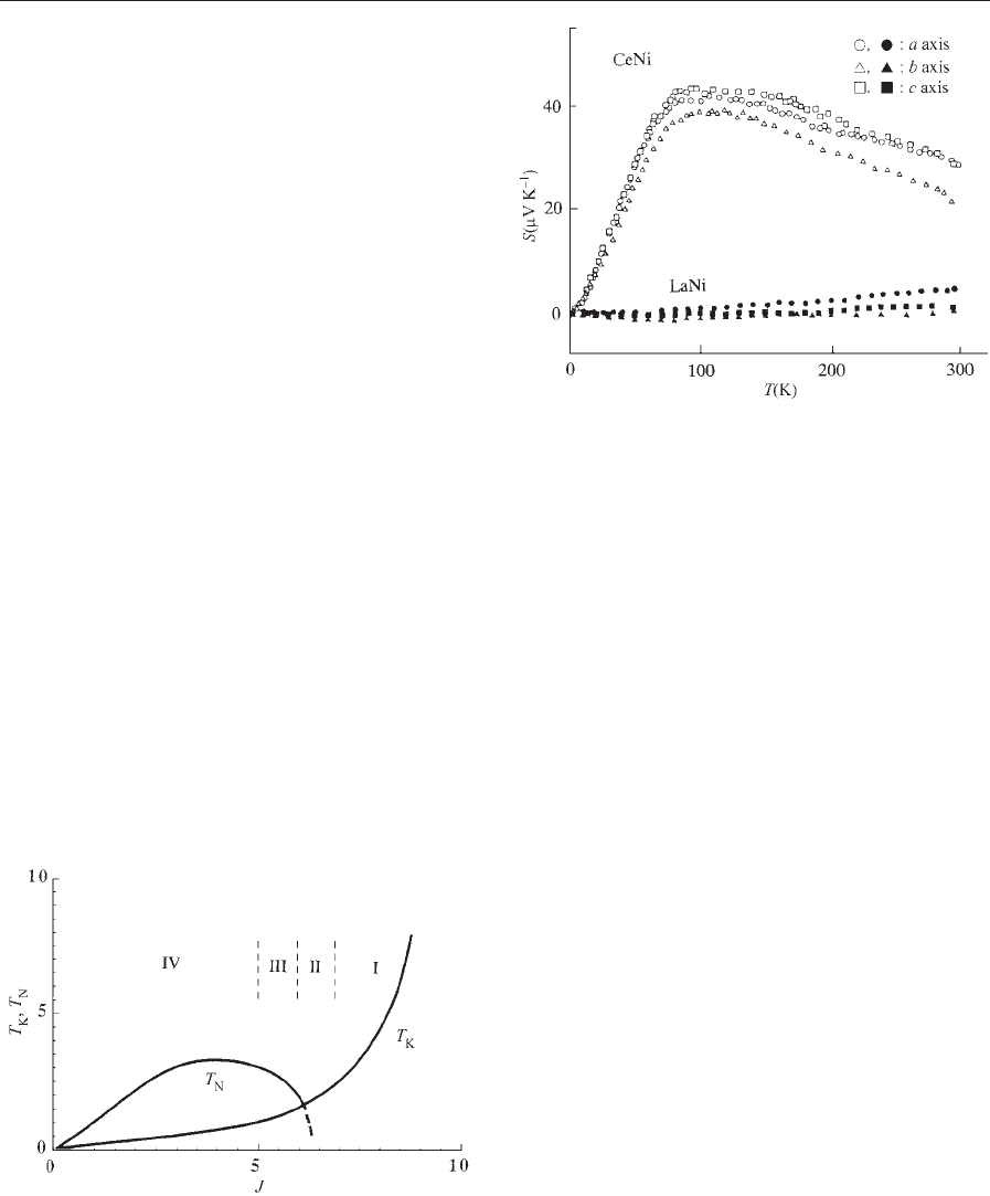
) are exemplified in Fig. 1 as functions of the hy-
bridization strength, J, between the cerium 4f elec-
trons and the conduction electrons. We can
distinguish in Fig. 1 four regions, I–IV, where ceri-
um compounds have distinctly different physical
properties. In region I, where T
K
bT
N
(or T
C
),
cerium compounds are in a fluctuating or inter-
mediate valence state, thus exhibiting no magnetic
moment in a wide temperature range ToT
K
.In
region II, with T
K
ET
N
or T
C
, the compounds lose
the magnetic moment of their localized Ce
3 þ
ions
owing to the hybridization between the cerium 4f
electrons and the conduction electrons, and the
effective masses of the electrons become very large
(heavy fermion) for ToT
K
. In region III, where T
K
is
slightly smaller than T
N
, cerium compounds order
magnetically with reduced ordered moments owing
to the Kondo effect. Finally, in region IV, where
T
K
5T
N
, cerium compounds are in an almost unper-
turbed antiferromagnetic state with the magnetic
moment determined from crystal field effects experi-
enced by the local Ce
3 þ
ion.
The S(T) curves for a CeNi single crystal are
shown in Fig. 2 as a typical compound of region I
together with the nonmagnetic LaNi reference sample
(Sakurai et al. 1996). The absolute values of S for
LaNi along the three principal axes of the ortho-
rhombic crystal are small, and the S(T) curves behave
nearly linearly. This behavior can be approximated
by the linear relationship S(T) ¼aT, where a ¼const.
over a wide temperature range. This formula can be
derived from the Boltzmann equation for normal
metals (see also Boltzmann Equation and Scattering
Mechanisms, and Kondo Systems and Heavy Fermi-
ons: Transport Phenomena), with the constant a ba-
sically representing conduction electron properties at
the Fermi level, described by the density of states
(DOS) function (Ziman 1960).
On the contrary, the absolute values of S for CeNi
along the three principal axes are much larger than
those for LaNi, and the S(T) curves exhibit broad
peaks with maximums around 100 K, indicating that
a is not a constant but depends on T. An enhance-
ment of the DOS takes place at the Fermi level owing
to the formation of nonmagnetic Kondo singlets at
low temperatures. Thus, a is much larger for CeNi
than for LaNi. With the increase of T, the thermal
excitation breaks the Kondo state causing a gradual
recovery of the cerium magnetic moments, hence the
value of a decreases. A gradual recovery of the Curie–
Weiss law is known to take place when T is larger
than the temperature of the maximum in S vs. T.In
this scenario the Kondo interaction predominates by
far over the RKKY interaction, and the effect of the
crystalline electric field (CEF) has not been taken into
account. Additional examples of these types of ma-
terials are CeSn
3
, CePd
3
, CeNiAl
4
, and CeNi
2
Ge
2
(Sakurai et al. 1996).
The S(T) curves of CeCu
6
(Onuki and Komatsu-
bara 1987) and CePtIn (Fujii et al. 1987) are shown in
Figure 1
Kondo temperature, T
K
, and the Neel temperatures, T
N
,
plotted as a function of the hybridization, J, between
cerium 4f electron and the conduction electron band
(after Doniach 1977).
Figure 2
S of an intermediate valence compound CeNi and its
nonmagnetic counterpart LaNi (single crystals) along
three crystal axes plotted as a function of temperature, T.
1079
Rare Earth Intermetallics: Thermopower of Cerium, Samarium, and Europium Compounds