Bichop R.H. (Ed.) Mechatronic Systems, Sensors, and Actuators: Fundamentals and Modeling
Подождите немного. Документ загружается.

20-124 Mechatronic Systems, Sensors, and Actuators
spectral response, which peaks at a wavelength about hc/E
g
. Photoresistors and junction detectors are
discussed in more detail in the following sections.
Photoresistors
The electrical conductivity of a semiconductor is the sum of two terms [5], one contributed by electrons
and the other by holes, as follows:
(20.77)
Each term is proportional to n(p) the number of electrons (holes) per unit volume in the conduction
(valence) band, the electron (hole) mobility
µ
n
(
µ
p
), and the magnitude of the charge of the electron e.
The increase in conductivity, caused by the absorption of photons increasing n and p, is the basis for the
operation of the photoresistive detector. This consists of a slab of semiconductor material on the faces
of which electrodes are deposited to allow the resistance to be monitored, as illustrated in Figure 20.103.
The photon-induced current is proportional to the length of the electrodes and inversely proportional
to their separation, hence the typical comb-like electrode geometry of photoresistors, shown in Figure
20.73. Because the resistance R
C
is inversely proportional to conductivity, the variation of R
C
with incident
power P
D
is very nonlinear and is often expressed in the form
(20.78)
where a and b are constants. Cadmium sulfide is commonly used as a detector of visible radiation because
it is low cost and its response is similar to that of the human eye. Other photoconductive materials include
lead sulfide, with a useful response from 1000 to 3400 nm, indium antimonide with a useful response
out to 7000 nm, and mercury cadmium telluride with peak sensitivity in the range 5000–14,000 nm.
The wavelength range 5000–14,000 nm is of importance because it covers the peak emission from bodies
near and above ambient temperature and also corresponds to a region of good transmission through the
atmosphere. Photoconductive devices used for the detection of long wavelength infrared radiation should
be cooled because of the noise caused by fluctuations in the thermal generation of charge. As a rough
rule of thumb, because of the Boltzmann factor, a detector with energy gap E
g
should be cooled to a
temperature less than E
g
/25k.
Junction Detectors
In photoresistors, the rate of generation of electron–hole pairs by the absorption of radiation, combined
with recombination at a rate characteristic of the device, results in an increase in free charge and therefore
electrical conductivity. In junction photodetectors [6], such as photodiodes and phototransistors, newly
generated electron–hole pairs separate before they can recombine so that a photon-induced electric
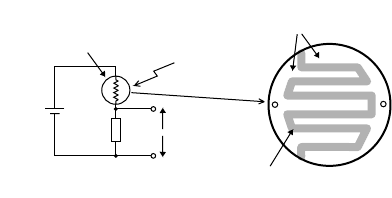
FIGURE 20.103 A simple light detector circuit employing a photoresistor is shown. An increase in light illumination
causes the resistance of the photoresistor to decrease and the output voltage to increase. The comb-like pattern
typically employed in photoresistors gives a relatively large active area of photoconducting material and a small electrode
spacing resulting in high sensitivity.
R
L
Incident
radiation
Output
voltage
Photoresistor
Bias
v
oltage
Evaporated
metal electrodes
Photoconducting
material
σ
ne
µ
n
pe
µ
p
+=
log
10
R
C
ablog P
D
–=
9258_C020_Sect_7-9.fm Page 124 Tuesday, October 9, 2007 9:09 PM
Sensors 20-125
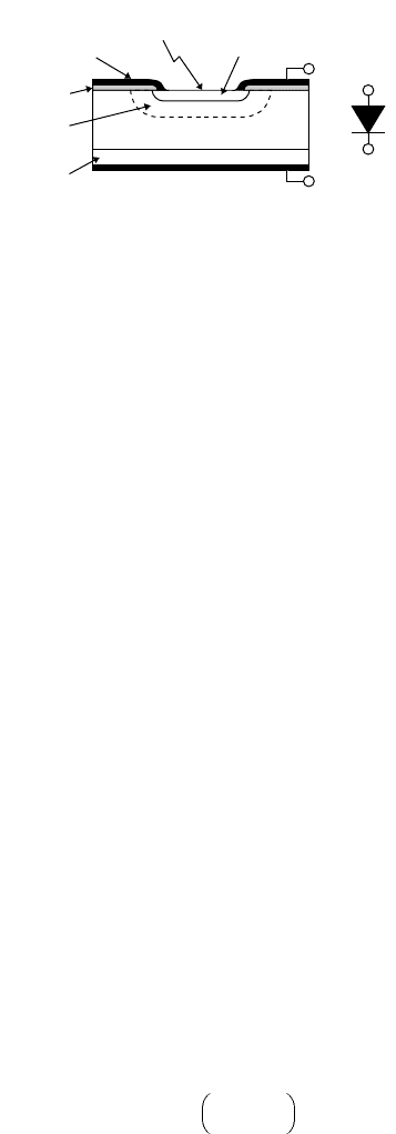
current can be detected. The separation of electrons and holes takes place in the electric field associated
with a P–N junction fabricated in a semiconductor material, which is usually silicon. The structure of a
typical silicon photodiode is shown in Figure 20.104. The substrate material is lightly doped n-type
silicon, which is pure group IV silicon into which has been added a small amount of a group V impurity
element. This contributes free electrons to the conduction band of the silicon leaving the impurity atoms
ionized and with a positive charge. A region of heavily doped p-type silicon is formed on the top face of
the substrate by adding a group III impurity element, by diffusion or ion implantation for example. The
group
III atoms contribute free holes to the valence band leaving negatively charged impurity ions. The P–N
junction is the boundary surface between the p-type and n-type regions on which the opposite impurity
concentrations are equal. The mobile electrons and holes diffuse across the boundary from the side
where they are in the majority, to the side where they are in the minority. There they recombine leaving
a region containing unscreened positive impurity ions on one side of the junction and a region containing
unscreened negatively charged impurity ions on the other. The charged region is called the space charge
or depletion region, because it is depleted of free charge. The movement of mobile charge continues until
the diffusion driving force is balanced by the opposing electric field created in the depletion region by
the separation of charge. When equilibrium has been established, the voltage across the depletion region,
called the built-in voltage, is about 0.6 V (for silicon). The depletion region extends much further into
the n-type silicon than into the p-type silicon for the photodiode shown in Figure 20.104 because of the
very different doping concentrations. The p-type region is made very thin, so that radiation can pass
through it, and metallic contacts are made to the p-type and n-type materials. An ohmic contact forms
between a metal and heavily doped silicon and to ensure a good ohmic contact to the lightly doped n-
type material, an intermediate more heavily doped n-type region is included as shown.
Electron–hole pairs formed in the depletion region when light with wavelength less than hc/E
g
is
absorbed are separated by the electric field in this region and can be detected in two ways. If the photodiode
is left open circuit, a voltage V
p
appears across the diode, varying logarithmically with the incident
irradiance P
D
as follows:
(20.79)
where
η
is the probability of a photon being absorbed, A is the active area of the photodiode, and i
0
is
the dark current due to thermal generation. This is the photovoltaic mode of operation. If the diode is
operated with a reverse bias, a photon-generated current i
p
flows given by the following expression:
(20.80)
FIGURE 20.104 The basic structure of a typical silicon photodiode is illustrated. A space charge, or depletion
region, is formed by the diffusion of mobile charge across the surface between the p-type and n-type silicon. It
extends furthest into the n-type silicon because this is more lightly doped than the p-type silicon. Any electron hole
pairs generated in this region are prevented from recombining by the presence of the electric field, which sweeps
them apart, allowing them to contribute to the photon generated current. The p-type region is made thin to allow
photons to penetrate into the depletion region.
Insulation
Metal contact
Incident
radiation
n silicon
p
+
silicon
Depletion
region
n
+
silicon
Symbol
+ + + + + + + + + + +
_ _ _ _ _ _ _ _ _ _ _
V
p
kT
e
------
η
P
D
Ae
λ
hci
0
--------------------
ln=
i
p
η
P
D
Ae
λ
hc
--------------------
=
9258_C020_Sect_7-9.fm Page 125 Tuesday, October 9, 2007 9:09 PM
20-126 Mechatronic Systems, Sensors, and Actuators
In this photoconductive mode, the current through the photodiode varies linearly with light irradiance.
The dark current i
0
varies rapidly with temperature and limits the sensitivity of the device but the photo-
conductive mode generally has faster response, better stability, and wider dynamic range than the photovoltaic
mode. The responsivity K
D
of the detector is defined by the relation i
p
= K
D
P
D
and is less than 1 A W
−1
for
a silicon diode. In the ideal case, K
D
varies linearly with wavelength, according to Equation 20.80, up to
the threshold value set by the energy gap. Photodiodes are available with a wide variety of characteristics
differing in sensitivity (area), speed of response, spectral response, and acceptance angle. They are available
with single devices or multiple devices (quad, linear array) in a single package.
The output signals from photodiodes needs amplification for many applications. This may be provided
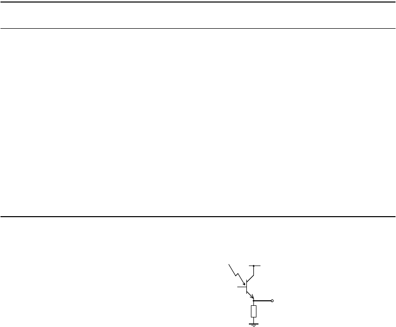
by a separate amplifier or by providing internal gain as in the phototransistor. This is constructed so that
radiation can fall on the base region of the transistor and the resulting base current is then internally
amplified. Often there is no external connection to the base and the amplified photocurrent is monitored
using the simple circuit shown in Figure 20.105. A typical phototransistor has a responsivity several
hundred times higher than that of a photodiode but the frequency response is relatively poor. Phototrans-
istors are often integrated with a spectrally matched LED into a single sensor package to act as a proximity
sensor, as in end-of-tape sensors, coin detectors, and level sensors. For reference, the characteristics of
several different types of discrete light detector are listed in Table 20.6.
By fabricating many small light detectors in a closely spaced array, it is possible to measure light
intensity at an array of points over a region. This is ideal for electronic imaging applications involving
video and still cameras. Image sensors designed for this purpose are discussed in the section titled ‘‘Image
Sensors,” but first it is useful to consider the formation of the images which the detectors sense.
TABLE 20.6 The Characteristics of a Number of Different Types of Light Detector
Description Active Region Response Spectral Response Dark Current
Response
Time
Acceptance
Angle
Medium
area silicon
photodiode
41.3 mm
2
0.5 A W
−1
peak
800 nm peak, range
350–1100 nm
4 nA 25 ns NA
Ultra high
speed silicon
photodiode
0.5 mm
2
0.35 A W
−1
800 nm peak, range
400–1000 nm
10 nA 1 ns NA
Filtered silicon
photodiode
7.5 mm
2
7 nA lux
−1
560 nm peak, range
460–750 nm
2 nA 3.5
µ
s 100°
16 photodiode
array on
1 mm pitch
Each diode
0.66 mm
2
0.6 A W
−1
900 nm peak, range
400–1100 nm
0.1 nA 4 ns NA
Silicon
phototransistor
0.7 mm
2
9 µA lux
−1
880 nm peak, range
450–1100 nm
0.3
µ
A 15
µ
s30°
Silicon
phototransistor
0.7 mm
2
2 µA lux
−1
880 nm peak, range
450–1100 nm
0.3
µ
A 15
µ
s80°
CdS
photoconductor
6.3 mm dia. 9 kΩ at 10 lux,
400 Ω at
1000 lux
530 nm peak NA 100 ms NA
FIGURE 20.105 A simple phototransistor light detec-
tor circuit is shown. Photon-generated current flowing
in the base-collector diode may be amplified several hun-
dred times by transistor action. Although the photon-
generated current is much larger than in an equivalent
photodiode, response time of the phototransistor is
much longer.
R
L
Incident
radiation
Base not
connected
Output
voltage
+ V
9258_C020_Sect_7-9.fm Page 126 Tuesday, October 9, 2007 9:09 PM
Sensors 20-127
20.8.5 Image Formation
Although perfect images are formed by small pinholes, lenses are needed to form bright images and
range from simple single-component lenses used to increase the amount of light falling on a single
detector or in low-cost cameras to complex zoom lenses, with between 14 and 20 components, capable
of producing high quality images of varying size. The two most important properties of a lens are its
focal length f, which determines the imaging behavior, and its light-gathering power or speed, specified
by an f-number f
#
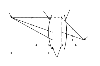
. A lens has an optical axis passing through the central axis of each of its components
along which a ray of light passes without deviation. A lens is characterized, regardless of its complexity,
by six cardinal points [2] spaced along the optical axis as illustrated in Figure 20.106, for a positive
converging lens. The position and magnification of the image of an object can be determined using these
cardinal points, which include two focal points, two nodal points, and two principal points. The nodal
points have the property that a ray outside the lens travelling towards one nodal point emerges from the
lens in a parallel direction, appearing to come from the other nodal point. The focal point is the point
which a ray of light incident on the lens parallel and close to the optical axis converges to (positive lens)
or diverges from (negative lens) after passing through the lens. The point where the lines colinear with
the ray on the two sides of the lens intersect defines a point on the principal plane. The point where the
optical axis intersects the principal plane is called the principal point. There are two nodal points, focal
points and principal planes, because light can be incident on the lens from either side. The front and
back focal lengths of the lens are the distances between the front and back focal points and their
corresponding principal planes. In the normal situation, when the lens is operating in a single medium,
such as air, the positions of the nodal points and principal points coincide and the front and back focal
lengths are equal. In general, when the lens construction is asymmetric, the front and back focal points
are at different distances from the corresponding external lens surface. In the case of an ideal thin lens,
the principal planes coincide with the lens center but in multi-element lenses they may be separated by
+20 to −10 mm, depending on the lens design. A lens of focal length f produces an image in best focus
at a distance v when the object is at distance u where
(20.81)
and the distances are measured to the corresponding principal planes. The image magnification
m
, defined
as the ratio of image to object sizes, is equal to the ratio of the image to object distances and is related to
FIGURE 20.106 The cardinal points of a multi-element lens operating in a single medium (usually air) are indicated.
The principal points and nodal points then coincide at N
1
and N
2
and the front and rear focal lengths are equal (f ).
Three rays from an object point are traced through the lens to the corresponding image point using the properties
of the cardinal points. In the case shown the image magnification is 0.5, so the image is some distance behind the
rear focal point F
2
. For distant objects the image plane would coincide with the plane transverse to the optical axis
passing through F
2
. Lenses are normally corrected for aberrations assuming that the object distance will be greater
than the image distance. In this case, for close-up work when the image distance is greater than the object distance,
the image quality is improved by reversing the lens.
Image
point
Principal
planes
Working distance
Rear lens
surface
ff
F
1
N
1
N
2
F
2
Front lens
surface
Object
point
Optical axis
1
u
---
1
v
--
+
1
f
--
=
9258_C020_Sect_7-9.fm Page 127 Tuesday, October 9, 2007 9:09 PM
20-128 Mechatronic Systems, Sensors, and Actuators
the total distance between object and image
D
T
by
(20.82)
where D
N
is the separation between the principal planes. Lenses generally have a focusing range around
5–10% of the focal length giving a maximum magnification of 0.05–0.1. For larger magnifications
extension rings can be fitted between the lens and sensor mounting. The extension size required, with
the lens focused at infinity, is simply the product of the magnification and the focal length, since image
distance is f(m + 1). When a lens is focused to produce an optimally sharp image for a particular object
distance u, there is range of closer and further object distances over which the image is still acceptably
sharp. This range is called the depth-of-field or depth-of-view F
o
and its size depends on the f-number
of the lens, the magnification, and the acceptable blur spot size C in the image plane [7]. The blur spot
size depends on the image sensor and for 35 mm film C is usually assumed to be between 0.02 and
0.033 mm, while for an image sensor array C is the separation between the individual detector elements,
typically about 0.01 mm. Depth-of-field decreases with magnification and for m greater than 0.1 is
calculated using the following formula:
(20.83)
The accuracy of alignment required of the image sensor depends on the depth-of-focus F
i
, which is the
longitudinal range of image positions over which the image is acceptably sharp. Sensor alignment is most
critical when the lens f-number is small and the image magnification is also small. When m is small F
i
reduces to 2Cf
#
v/f and equals m
2
F
o
. When m is large, the depth-of-focus is not so critical.
It is frequently necessary to relate the lighting of a scene to the image irradiation falling on a sensor.
As accurate calculations are difficult, it is usually best to make a simple estimate and then make fine
adjustments to the lighting or lens aperture. When the object of interest in the scene is not a light source
but is visible because it is reflecting light, then its luminance must be estimated from the radiation falling
on it and the reflection coefficient R
o
of its surface [3]. For example, if the object is a Lambertian surface,
with illumination L
o
, then its luminance is given by
(20.84)
When a lens is used to form an image of the object, the illuminance on the optical axis in the image
plane L
S
in lux is related to the luminance of the object B in cd m
−2
by
(20.85)
where f
#
is defined as the ratio of the focal length to diameter of the effective lens aperture and losses in
the lens are characterized by a transmission coefficient T [7]. Due to a number of geometrical factors,
the image illumination falls off with angle
θ
from the optic axis as cos
4
θ
. Near the axis, the illuminance
varies only slowly with angle but at an angle of 30° it has fallen by 44%. Equation 20.85 is the basis for
rating the speed of lenses by their f-numbers and indicates that the smaller the f-number, the greater the
image illuminance. This formula is appropriate when the magnification is small, but for close-up work,
when the image distance is significantly greater than the focal length, the f-number f
#
should be replaced
by (m + 1)f
#
when calculating image illuminance.
D
T
fm 1+()
2
m
----------------------
= D
N
+
F
o
2f
#
Cm 1+()
m
2
----------------------
=
BL
o
R
o
π
-----
=
L
s
TB
π
2f
#
m 1+()[]
2
--------------------------------=
9258_C020_Sect_7-9.fm Page 128 Tuesday, October 9, 2007 9:09 PM

Sensors 20-129
Lenses are manufactured to match standard image sizes such as the 36 mm × 24 mm 35 mm photo-
graphic format and the standard television sensor sizes 1″, 2/3″, 1/2″, 1/3″, and 1/4″. These sizes are
defined to be twice the horizontal dimension of a rectangular image with 4:3 aspect ratio so that, for
example, a 1″ sensor has a width of 12.7 mm, a height of 9.5 mm, and a diagonal length of 15.9 mm.
Lens sizes are similarly specified to allow easy matching of lenses to sensors. The maximum angular field-
of-view F
OV
of a lens focused at infinity is given by
(20.86)
where C
F
is the diagonal of the sensor format. For example, a 35-mm lens with a focal length of 55 mm
has a field of view of 43°. Because image distortion and sharpness worsen towards the edges of the field
of view it is acceptable, for example, to use a 2/3″ lens with a 1/2″ sensor, but not the converse. A 35-mm
camera lens generally performs much better, at relatively low cost, than a corresponding C-mount lens
supplied for a TV camera but a C-mount to Pentax, Cannon, or Nikon mount converter is then required.
20.8.6 Image Sensors
The generation of an output signal from a standard image sensor involves up to four operations: the
conversion of the spatial distribution of light irradiance in the image plane into a corresponding spatial
distribution of charge; the accumulation and storage of this charge near the point where it is generated;
the transfer or read-out of this charge; and the conversion of the charge to an output voltage signal. Each
of these operations can be achieved in many ways. Vacuum tube sensors such as vidicons, for example,
use a photoconductive detector material and a scanning electron beam for read-out while CMOS sensors
use a photodiode detector and a readout bus. Solid state devices are currently the most widely used types,
so only CCD and CMOS sensors are considered here. In these devices the image irradiance is measured
on a one- or two-dimensional array of sample regions with positions fixed during fabrication. Each
sample is called a picture element or pixel and the greater the number of pixels, the higher the resolution
with which the image can be recorded. Area sensors are manufactured with numbers of pixels ranging
from tens of thousands to several million. Color sensors are achieved by placing color filters over the
individual pixels, in a mosaic or stripe pattern, and interpolating the color values at pixels where necessary
from the neighboring values. In such color devices the color resolution is lower than the luminance
resolution, but this is not important for many applications because the resolution of the human eye is
worse for color than for luminance. More expensive color cameras use three precisely aligned sensors,
one for each primary color. Cameras incorporating such sensors generally produce either a television
standard signal [8] (RS-170 monochrome and NTSC color for 525 American television or CCIR mono-
chrome and PAL color for European television) or a digital signal such as RS-423, USB or IEE 1394 Fire
Wire, which can be readily connected to a computer.
20.8.6.1 Charge-Coupled Devices
In a charge-coupled device [9] an isolated packet of charge, of between 10 and 10
6
electrons, is moved
through the semiconductor, from a position in one CCD cell to a position in an adjacent cell, by applying
a sequence of voltage pulses to gate electrodes. In CCD-based light sensors, photon generated charge
packets accumulate in photosites, which are modified CCD cells, and are then transported through other
CCD cells to another modified cell with a readout amplifier attached. A CCD is fabricated on a single
crystal wafer of P-type silicon and consists of a one- or two-dimensional array of charge storage cells,
on centers typically about 10
µ
m apart. The operation of a 3-phase CCD cell is illustrated in Figure
20.107. Each cell has three closely spaced electrodes (gates) on top, insulated from the silicon by a thin
layer of silicon dioxide. A positive voltage applied to one of these gates will attract and store any free
charge generated in the silicon due to light or thermal action while free holes are repelled and collected
by the substrate electrode. Lower voltages on the adjacent gates isolate it from the neighboring cells,
F
OV
2tan
−1
=
C
F
2f
------
9258_C020_Sect_7-9.fm Page 129 Tuesday, October 9, 2007 9:09 PM
20-130 Mechatronic Systems, Sensors, and Actuators
creating a localized potential well within the cell. A cell of size 8 µm × 8 µm can hold about 200,000
electrons before saturating. Cells designed to be light sensitive have electrodes made of semitransparent
polysilicon so that light can penetrate into the storage region, while cells intended only for charge
transport are covered with a surface layer opaque to light. During operation, the voltages on the electrodes
are held constant for a time (integration time) to allow packets of charge to accumulate on the photosites
in proportion to the local irradiance. At the end of this time a sequence of voltage pulses are applied to
the electrodes to transfer the packets of charge from one storage cell to the next until they reach a sensing
amplifier, which generates a voltage which is about 0.6
µ
V per electron. The charge transfer efficiency
(CTE) of real devices is less than 100% and between 99.95% and 99.999% of the stored charge is moved
to the next cell, depending on the precise construction and clocking frequency. This allows devices to be
manufactured with a line of many hundreds or thousands of storage cells feeding a single amplifier.
Although there are many variations in CCD construction, the basic characteristics of CCDs from
different manufactures are similar. CCD light sensors have an inherently linear variation of output voltage
with irradiance, from the minimum useful level set by noise to the maximum useful level set by saturation
of the output amplifier or by the limited capacity of the charge storage cells. The dynamic range of the
device is defined as the ratio of the maximum output signal to the output resulting from noise. Manu-
facturers sometimes quote noise figures as peak-to-peak or as root-mean-square values (typically five
times smaller), but the former value is more relevant for imaging applications. Due to manufacturing
limitations, the photosites do not have identical sensitivity and dark signal characteristics. For example,
photoresponse nonuniformity (PRNU) is easy to measure using uniform sensor illumination and is
typically 5–10%. Its effects can be removed, if necessary, by calibration. The basic spectral response of a
silicon sensor extends from 200 to 1100 nm, with a maximum sensitivity of about 1
µ
A of generated
charge per microwatt of incident radiation, but this is modified by the electrode structures formed on
the surface of the silicon. Longer wavelength photons penetrate more deeply than shorter wavelength
photons and the short wavelength response is typically worsened to 450 nm by absorption in the surface
layers. Infrared photons may generate electrons some distance from the point of entry into the silicon,
with the result that the charge may be collected by a different cell. This reduces the resolution of the
device and if infrared operation is not required, but the illumination contains infrared (for example, from
a tungsten lamp), an infrared reflecting filter (a hot-mirror filter) is often used. If the widest possible
spectral response is required, devices have the substrate thinned and are operated with the illumination
falling on the back surface, which is free of electrodes. Back illuminated devices are fragile and costly but
are used in specialist low-light applications like astronomy and biology.
FIGURE 20.107 The movement of charge from one potential well to the next in a 3-phase CCD is illustrated. Each
CCD cell has three gate electrodes. In the upper potential diagram, the well is formed under the first electrode in
each CCD cell by voltage applied to the phase 1 line. As the voltage is reduced on the phase 1 line and increased on
the phase 2 line, the original potential wells collapse and new ones form under the second gate in each cell, causing
any charge present in the wells to move sideways as indicated. Two more cycles are required to complete the movement
of charge into the first well of the next CCD cell.
Phase 3
Phase 2
Phase 1
P-type silicon substrate
1/3 cycle
Potential
well
Insulating layer
Gate
electrode
9258_C020_Sect_7-9.fm Page 130 Tuesday, October 9, 2007 9:09 PM
Sensors 20-131
All CCD cells accumulate charge linearly with time due to thermally generated electrons produced
within the cells and at electrode interfaces. Like the photoresponse, this dark signal varies from cell to
cell and can be compensated for by calibration. These thermally generated contributions are most sig-
nificant for low-light level applications and can be reduced by cooling the sensor using either a thermo-
electric cooler, a Joule Thomson cooler, or a liquid nitrogen dewar. The dark signal reduces by 50% for
every 7°C reduction in temperature and at −60°C, produced by a Peltier cooler, the dark signal is typically
reduced to about one electron per pixel per second. Another important temperature dependent charac-
teristic of the CCD sensor, which improves with cooling, is the noise floor of the output amplifier which
is proportional to T
1/2
and typically equivalent to about 300 electrons at room temperature. A CCD
device used in astronomy illustrates the performance achieved by cooling. Operated at about
–
110°C,
this device has a readout noise of about 10 electrons, a dark current less than 0.3 electrons per minute,
and a quantum efficiency for converting visible photons into electrons of between 70% and 80%. Light
may be integrated for periods of hours compared with the approximately 1/8 s to 1/4 s integration period
of the dark adapted eye. Compared with photographic film previously used for low-light level imaging
in astronomy, cooled CCDs are from 10 to 100 times more sensitive, linear in response rather than
nonlinear, and have a much greater dynamic range so that both faint and bright objects can be recorded
in the same exposure.
The transfer of charge from one cell to the next takes time and the CTE worsens with increasing
clocking speed and with cooler temperatures. This limits the number of cells which can be used to
transport charge from a photosite to the readout amplifier. It also limits the rate at which data can be
transferred out of the CCD and the resulting image transfer rate. However, there are many variations in
CCD technology aiming to improve performance. For example, virtual-phase CCDs [10] have some of
the electrodes replaced by ion-implanted regions resulting in improved blue response and higher sensi-
tivity, because of the removal of some of the blocking surface gates and simpler drive circuitry due to
the lower number of gates per cell. The biggest contribution to the dark signal is defects at interfaces
and a manufacturing technique known as pinning can be used to passivate the interface states, producing
an order of magnitude improvement in a dark signal as well as improved quantum efficiency and CTE.
The readout noise performance can be improved by a signal-processing technique called correlated double
sampling. This involves taking the output as the difference between two signals, one with the charge
signal present and one without, so that major noise components are cancelled. A number of architectures
are employed in CCD devices [11]. Several of these, including linear devices and area devices of the full-
frame, frame transfer, and interline transfer types, are discussed in the following sections.
Linear Charge-Coupled Devices
A linear CCD sensor consists of a line of up to several thousand photosites and an adjacent parallel CCD
shift register terminated by a sensing amplifier. Each photosite is separated from a shift register cell by
a transfer gate. During operation a voltage is applied to each photosite gate to create empty storage wells,
which then accumulate amounts of charge proportional to the integral of the light intensity over time.
A transfer pulse at the end of the integration period causes all the accumulated charge packets to be
transferred through the transfer gates to the shift register cells. The charges are clocked through the shift
register to the sensing amplifier producing a sequence of voltage pulses with amplitudes proportional to
the integrated light falling on the photosites. In practice it is common for shift registers to be placed on
both sides of the photosites with alternate photosites connected by transfer gates to the right and left
registers. These halve the time required to clock out all the data. There is a limit to the number of electrons
(typically 1000–2000 times the area of the photosite in
µ
m
2
) which can be stored in a cell, before electrons
start to spill over into adjacent cells. This blooming effect is a problem with images containing intense
highlights. It is reduced by about a factor of 100 by adding antiblooming gates between adjacent photosites
and transfer gates and channel stops between adjacent photosites. The voltage on the antiblooming gates
is set at a value which allows surplus charge to drain away instead of entering the transfer gates and shift
register. By clocking this voltage, variable integration times which are less than the frame pulse to frame
pulse exposure time can also be attained.
9258_C020_Sect_7-9.fm Page 131 Tuesday, October 9, 2007 9:09 PM
20-132 Mechatronic Systems, Sensors, and Actuators
Area Charge-Coupled Devices
Three basic architectures are used in area CCDs and are illustrated in Figure 20.108. The full-frame CCD
consists of an imaging area separated from a horizontal CCD shift register by a transfer gate. In the
imaging area each photosite is one stage of a vertical shift register separated from neighboring shift
registers by channel stops and anti-blooming structures. During the light integration period, the vertical
clocks are stopped and the photosites collect photoelectrons. At the end of this period the charge is
clocked out vertically, one row at a time into the horizontal shift register. The charge in the horizontal
shift register is then very rapidly shifted towards the output amplifier by the application of a horizontal
clock signal. For example, the RA1001J, 1024 × 1024 pixel full-frame CCD from EG&G Reticon achieves
a readout rate of 30 frames per second. To avoid image smear during the readout period, full-frame
sensors must be operated with external shutters or used in low-light level applications requiring very
long integration times compared with the readout time, as in astronomy.
The frame-transfer CCD greatly reduces the need for an external shutter by providing a light-shielded
storage section into which the entire image charge is shifted at a rate limited primarily by CTE consider-
ations. The charge is read from the storage region during the next integration period without any further
image smearing. In some devices, such as the EG&G Reticon RA1102, the storage area is split into two
on opposite sides of the imaging area. This improves performance by halving the maximum number of
transfers required to reach the nearest storage region. With sensors designed for interlaced operation, as
opposed to the non-interlaced progressive scan readout mode, this reduction occurs automatically. Each
integration period then corresponds to one video field and only half the number of rows in the frame is
required at any one time. For example, to produce an interlaced video frame containing 576 image lines
(CCIR standard), a frame transfer sensor with only 288 rows of storage is required. By changing the clock
signals, the odd field can be displaced vertically by half a line width relative to the even field. This ensures
that the odd and even lines contain different information and reduces aliasing because the cell width is
twice the separation between the lines in the frame. Many companies produce frame-transfer CCD sensors
and cameras including Cohu, Dalsa, EG&G Reticon, EEV, Kodak, Philips, and Thomson-CSF.
The interline-transfer (ILT) architecture virtually eliminates image smear by providing each column
of photosites with an adjacent light-shielded vertical CCD shift register into which the charge is transferred
by a transfer pulse. The contents of all the vertical shift registers are then shifted simultaneously one
pixel at a time into a horizontal shift register where they are rapidly shifted to an output amplifier. This
approach makes it easy to achieve short integration times and true “stop-motion” exposure control with
progressive scan. It also increases the “dead space” between the active pixels reducing the sensitivity of
FIGURE 20.108 The three basic architectures used in area CCDs are illustrated. In the full-frame transfer CCD
most of the device area is employed as photosites. Photon-generated charge is transferred down each column one
cell at a time into the horizontal shift register where it must all be transferred to the readout amplifier before another
vertical movement of charge can take place. The frame-transfer CCD reduces the need for a mechanical shutter to
prevent charge smearing, which would otherwise occur, by providing a covered storage area into which all the photon-
generated charge can be rapidly shifted vertically at the end of the integration period. The interline-transfer CCD
allows all the photon-generated charge to be transferred to the covered vertical shift registers in one step, virtually
eliminating this source of charge smearing.
Full frame
CCD
Frame transfer
CCD
Interline transfer
CCD
Photosite
Covered
storage
area
Readout
amplifier
Photosite
Vertical shift
register
Horizontal
shift
register
9258_C020_Sect_7-9.fm Page 132 Tuesday, October 9, 2007 9:09 PM
Sensors 20-133
the image sensing area and increasing aliasing effects compared with frame-transfer sensors. For the
latter, the fill factor, which is the percentage of the imaging area which is light sensitive, can be close to
100% whereas it is usually less than 50% for interline-transfer devices. Localized bright objects tend to
produce vertical streaks in an ILT device because strong light can leak under the narrow light shield
covering the vertical shift registers, causing image smearing similar to that in a full frame device. For
interlaced operation, two adjacent pixels, for example, 1 and 2, 3 and 4, etc. are transferred to a single
shift register cell on one field and in the next field pixels 2 and 3, 4 and 5, etc. are transferred together.
This is rather similar to the interlaced operation of a frame transfer CCD. Many companies manufacture
ILT CCD sensors and cameras including, Hitachi, NEC, Panasonic, Pulnix, and Sony.
20.8.6.2 CMOS Sensors
CMOS image sensors are based on a technology that is older than CCD technology [12]. However, CCD
sensors originally offered better image quality than CMOS devices could match so they came to dominate
the market. There is now renewed interest in the older technology because it potentially offers major
advantages over CCDs. The CMOS process used in sensors is similar to that which has been highly
developed in order to manufacture dynamic RAM and consequently should be able to produce cheap,
small high-resolution, randomly addressed, low-power sensors. It is also possible to integrate image
sensing, control, processing, and interfacing on the same chip, so that a camera on a chip is possible using
CMOS technology, but not with CCD technology. As a result of recent research and development, several
manufacturers are now claiming to have achieved CMOS sensors providing similar quality to that of
mainstream CCDs. Manufacturers producing CMOS sensors include Fillfactory, National Semiconductor,
Philips, ST Microelectronics, and Y Media.
A CMOS sensor consists of an array of photodiodes, which are connected to readout amplifiers by
bus lines and MOS switches. The principle of readout is illustrated in Figure 20.109. Each pixel is
connected to an output amplifier by a switch whose control line is connected to a digital shift register.
Shifting a bit through the register connects the photodiodes sequentially to the output amplifier. Random
readout of the photodiodes can be achieved by replacing the shift register by an address decoder connected
to an address bus. Two-dimensional arrays of photodiodes are connected in a configuration similar to a
cross-point switching matrix with a switch and diode at each cross point and separate vertical and
horizontal shift registers. To scan the array, the vertical shift register turns on a complete row of switches
and the photodiodes in that row output their signals into vertical bus lines. These are connected, in turn,
FIGURE 20.109 The principle of readout in a one-dimensional CMOS sensor is illustrated. Each pixel is connected
to an output amplifier by a MOS switch whose control line is connected to the digital shift register. Shifting a bit
through the register connects the photodiodes, in turn, to the output amplifier.
FIGURE 20.110 A typical CMOS three-transistor active
pixel is shown. Transistor T
1
is connected to the reset line
allowing the capacitance of the photodiode to be reset at
the start of photo-current integration. In the continuous
mode CMOS device this transistor is connected to act as
high value resistor. Transistors T
2
and T
3
allow the signal
to be transferred from the photodiode to the column
amplifier, via the column bus line.
Digital shift register
Amplifier
MOS
switch
Photodiode
T
1
T
2
T
3
Reset
Row select
Photodiode
Column
bus
V
dd
9258_C020_Sect_7-9.fm Page 133 Tuesday, October 9, 2007 9:09 PM