Askeland D.R., Fulay P.P. Essentials of Materials Science & Engineering
Подождите немного. Документ загружается.


4
Imperfections in the Atomic
and Ionic Arrangements
Have You Ever Wondered?
9 Why silicon crystals, used in the manufacture of semiconductor chips, contain trace amounts of
dopants, such as phosphorous or boron?
9 What makes steel considerably harder and stronger than pure iron?
9 Why do we use very high-purity copper as a conductor in electrical applications?
9 Why FCC metals (such as copper and aluminum) tend to be more ductile than BCC and HCP
metals?
The arrangement of the atoms or ions in en-
gineered materials contains imperfections or
defects. These defects often have a profound
effect on the properties of materials. In this
chapter, we introduce the three basic types of
imperfections: point defects, line defects (or
dislocations), and surface defects. These imper-
fections only represent defects in or deviations
from the perfect or ideal atomic or ionic ar-
rangements expected in a given crystal struc-
ture. T he material is not considered defective
from an application viewpoint. In many appli-
cations, the presence of such defects actually
is useful. There are a few applications, though,
90

wherewewillstrivetominimizeaparticular
type of defect. For example, defects known
as dislocations are useful in increasing the
strength of metals and alloys. However, in sin-
gle crystal silicon, used f or manufacturing
computer chips, the presence of dislocations is
undesirable. Often the ‘‘defects’’ are created
intentionally to produce a desired set of elec-
tronic, magnetic, optical, and mechanical
properties. For example, pu re iron is relatively
soft, yet, when we add a small amount of car-
bon, we create defects in the crystalline a r-
rangement of iron and turn it into a plain car-
bon steel that exhibits considerably higher
strength. Similarly, a crystal of pure alumina
(Al
2
O
3
) i s transparent and colorless, but, when
we add a small amount of chromium (Cr), it
creates a special defect, resulting in a beautiful
red ruby crystal.
Grain boundaries, regions between different
grains of a polycrystalline material, represent one
type of defect that can control properties. For ex-
ample, the new ceramic superconductors, under
certain conditions, can conduct electricity without
any electrical resistance. Materials scientists and
engineers have made long wires or tapes of such
materials. They have also discovered that, al-
though the current flows quite well within the
grains of a polycrystalline superconductor, there is
considerable resistance to the flow of current from
one grain onto another—across the grain boun-
dary. On the other hand, the presence of grain
boundaries actually helps strengthen metallic ma-
terials. In later chapters, we will show how we can
control the concentrations of these defects
through tailoring of composition or processing
techniques. In this chapter, we explore the nature
and effects of different types of defects.
4-1 Point Defects
Point defects are localized disruptions in an otherwise perfect atomic or ionic arrange-
ments in a crystal structure. Even though we call them point defects, the disruption af-
fects a region involving several of the surrounding atoms or ions. These imperfections,
shown in Figure 4-1, may be introduced by movement of the atoms or ions when they
gain energy by heating, during processing of the material or by introduction of other
atoms. The distinction between an impurity and a dopant is as follows: Typically, im-
purities are elements or compounds that are present from raw materials or processing.
For example, silicon single crystals grown in quartz crucibles contain oxygen as an im-
purity. Dopants, on the other hand, are elements or compounds that are deliberately
added, in known concentrations, at specific locations in the microstructure, with an
intended beneficial e¤ect on properties or processing. In general, the e¤ect of impurities
is deleterious, whereas the e¤ect of dopants on the properties of materials is useful.
Phosphorus (P) and boron (B) are examples of dopants that are added to silicon crystals
to improve or alter the electrical properties of pure silicon (Si).
A point defect typically involves one atom or ion, or a pair of atoms or ions, and
thus is di¤erent from extended defects, such as dislocations, grain boundaries, etc. An
important ‘‘point’’ about point defects is that although the defect occurs at one or two
sites, their presence is ‘‘felt’’ over much larger distances in a crystalline material.
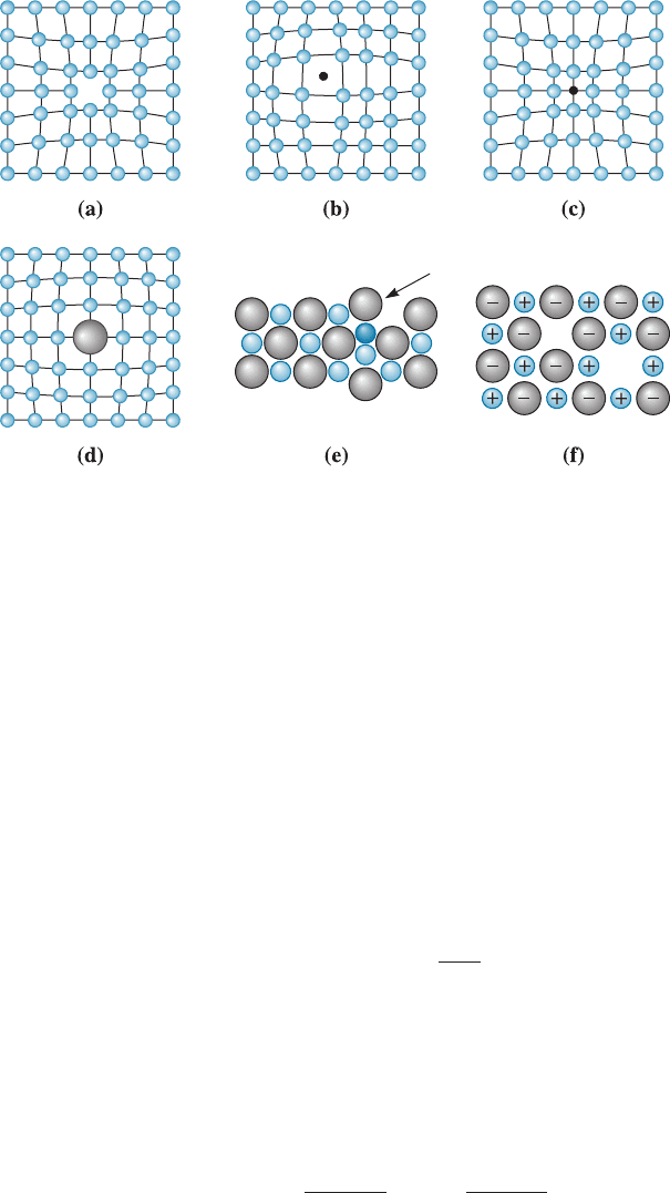
Vacancies A vacancy is produced when an atom or an ion is missing from its normal
site in the crystal structure, as in Figure 4-1(a). When atoms or ions are missing (i.e.,
when vacancies are present), the overall randomness or entropy of the material
increases, which increases the thermodynamic stability of a crystalline material. All
4-1 Point Defects 91
crystalline materials have vacancy defects. Vacancies are introduced into metals and
alloys during solidification, at high temperatures, or as a consequence of radiation
damage. Vacancies play an important role in determinin g the rate at which atoms or
ions can move around, or di¤use in a solid material, especially in pure metals. We will
see this e¤ect in greater detail in Chapter 5. In some other applications, we make use of
the vacancies created in a ceramic material to tune its electrical properties. This includes
many ceramics that are used as conductive and transparent oxides such as indium tin
oxide (ITO) and zirconia oxygen (ZrO
2
) sensors.
At room temperature (@300 K), the concentration of vacancies is small, but the
concentration of vacancies increases exponentially as we increase the temperature, as
shown by the following Arrhenius type behavior:
n
v
¼ n exp
Q
v
RT
ð4-1Þ
where
n
v
is the number of vacancies per cm
3
;
n is the number of atoms per cm
3
;
Q
v
is the energy required to produce one mole of vacancies, in cal/mol or
Joules/mol;
R is the gas constant, 1.987
cal
mol K
or 8.31
Joules
mol K
; and
T is the temperature in degrees Kelvin.
Due to the large thermal energy atoms have near the melti ng temperature of a
material, there may be as many as one vacancy per 1000 atoms. Note that this equation
provides for equili brium concentration of vacancies at a given temperature. It is also
Figure 4-1 Point defects: (a) vacancy, (b) interstitial atom, (c) small substitutional atom,
(d) large substitutional atom, (e) Frenkel defect, and (f ) Schottky defect. All of these defects
disrupt the perfect arrangement of the surrounding atoms and create a strain in the crystal
structure.
C H A P TE R 4 Imperfections in the Atomic and Ionic Arrangements92

possible to retain a non-equilibrium concentration of vacancies produced at a high tem-
perature by quenching the material rapidly. Thus, in many situations the concentration
of vacancies observed at room temperature is not the equilibrium concentration pre-
dicted by Equation 4-1.
EXAMPLE 4-1
The Effect of Temperature on Vacancy Concentrations
Calculate the concentration of vacancies in copper at 25
C. What temperature
will be needed to heat treat copper such that the concentration of vacan-
cies produced will be 1000 times more than the equilibrium concentration of
vacancies at room temperature? Assume that 20,000 cal are required to
produce a mole of vacancies in copper.
SOLUTION
The lattice parameter of FCC copper is 0.36151 nm. The basis is 1, therefore,
the number of copper atoms, or lattice points, per cm
3
is:
n ¼
4 atoms=cell
ð3:6151 10
8
cmÞ
3
¼ 8:47 10
22
copper atoms=cm
3
At 25
C, T ¼ 25 þ 273 ¼ 298 K:
n
v
¼ n exp
Q
v
RT
¼ 8:47 10
22
atoms
cm
3
exp
20;000
cal
mol
1:987
cal
mol K
298 K
0
B
B
B
@
1
C
C
C
A
¼ 1:815 10
8
vacancies=cm
3
We wish to find a heat treatment temperature that will lead to a concentration
of vacancies which is 1000 times higher than this number, or n
v
¼ 1:815 10
11
vacancies/cm
3
.
We could do this by heating the copper to a temperature at which this
number of vacancies forms:
n
v
¼ 1:815 10
11
¼ n exp
Q
v
RT
¼ð8:47 10
22
Þ expð20;000=ð1:987 T ÞÞ
exp
20;000
1:987 T
¼
1:815 10
11
8:47 10
22
¼ 0:214 10
11
20;000
1:987T
¼ lnð0:214 10
11
Þ¼26:87
T ¼
20;000
ð1:987Þð26:87Þ
¼ 375 K ¼ 102
C
By heating the copper slightly above 100
C, until equilibrium is reached, and
then rapidly cooling the copper back to room temperature, the number of
4-1 Point Defects 93

vacancies trapped in the structure may be one thousand times greater than the
equilibrium number of vacancies at room temperature. Thus, vacancy concen-
trations encountered in relatively pure materials are often dictated by both the
thermodynamic and kinetic factors.
EXAMPLE 4-2
Vacancy Concentrations in Iron
Determine the number of vacancies needed for a BCC iron crystal to have a
density of 7.87 g/cm
3
. The lattice parameter of BCC iron is 2:866 10
8
cm.
SOLUTION
The expected theoretical density of iron can be calculated from the lattice
parameter and the atomic mass. Since the iron is BCC, two iron atoms are
present in each unit cell.
r ¼
ð2 atoms=cellÞð55:847 g=molÞ
ð2:866 10
8
cmÞ
3
ð6:02 10
23
atoms=molÞ
¼ 7:8814 g=cm
3
We would like to produce iron with a density of 7.87 g/cm
3
. We could do this
by intentionally introducing vacancies into the crystal. Let’s calculate the
number of iron atoms and vacancies that would be present in each unit cell for
the required density of 7.87 g/cm
3
:
r ¼
ðX atoms=cellÞð55:847 g=molÞ
ð2:866 10
8
cmÞ
3
ð6:02 10
23
atoms=molÞ
¼ 7:87 g=cm
3
X atoms=cell ¼
ð7:87Þð2:866 10
8
Þ
3
ð6:02 10
23
Þ
55:847
¼ 1:9971
Or, there should be 2:00 1:9971 ¼ 0:0029 vacancies per unit cell. The number
of vacancies per cm
3
is:
Vacancies=cm
3
¼
0:0029 vacancies=cell
ð2:866 10
8
cmÞ
3
¼ 1:23 10
20
We assume that introduction of vacancies does not change the lattice constant.
If additional information, such as the energy required to produce a vacancy in
iron, is available, we might be able to design a heat treatment (as we did in
Example 4-1) to produce this concentration of vacancies.
Interstitial Defects An interstitial defect is formed when an extra atom or ion is in-
serted into the crystal structure at a normally unoccupied position, as in Figure 4-1(b).
The interstitial sites were illustrated in Table 3-5. Interstitial atoms or ions, although
much smaller than the atoms or ions located at the lattice points, are still larger than
the interstitial sites that they occupy. Consequently, the surrounding crystal region is
compressed and distorted. Interstitial atoms such as hydrogen are often present as im-
purities; whereas carbon atoms are intentionally added to iron to produce steel. For
small concentrations, carbon atoms occupy interstitial sites in the iron crystal structure,
introducing a stress in the localized region of the crystal in their vicinity. If there are
C H A P TE R 4 Imperfections in the Atomic and Ionic Arrangements94
dislocations in the crystals trying to move around these types of defects, they face a re-
sistance to their motion, making it di‰cult to create permanent deformatio n in metals
and alloys. This is one important way of increasing the strength of metallic materials.
Unlike vacancies, once introduced, the number of interstitial atoms or ions in the
structure remains nearly constant, even when the temperature is changed.
EXAMPLE 4-3
Interstitial Sites for Carbon in Iron
In FCC iron, carbon atoms are located at octahedral sites at the center of
each edge of the unit cell (1/2, 0, 0) and at the center of the unit cell (1/2, 1/2,
1/2). In BCC iron, carbon atoms enter tetrahedral sites, such as 1/4, 1/2, 0. The
lattice parameter is 0.3571 nm for FCC iron and 0.2866 nm for BCC iron.
Assume that carbon atoms have a radius of 0.071 nm. (1) Would we expect a
greater distortion of the crystal by an interstitial carbon atom in FCC or BCC
iron? (2) What would be the atomic percenta ge of carbon in each type of iron if
all the interstitial sites were filled?
SOLUTION
1. We could calculate the size of the interstitial site at the 1/4, 1/2, 0 location
with the help of Figure 4-2(a). The radius R
BCC
of the iron atom is:
R
BCC
¼
ffiffiffi
3
p
a
0
4
¼
ð
ffiffiffi
3
p
Þð0:2866Þ
4
¼ 0:1241 nm
Figure 4-2 (a) The location of the
1
4
,
1
2
, 0 interstitial site in BCC metals, showing
the arrangement of the normal atoms and the interstitial atom (b)
1
2
, 0, 0 site in
FCC metals. (c) Edge centers and cube centers are some of the interstitial sites in
the FCC structure. (For Example 4-3.)
4-1 Point Defects 95

From Figure 4-2(a), we find that:
1
2
a
0
2
þ
1
4
a
0
2
¼ðr
interstitial
þ R
BCC
Þ
2
ðr
interstitial
þ R
BCC
Þ
2
¼ 0:3125a
2
0
¼ð0:3125Þð0:2866 nmÞ
2
¼ 0:02567
r
interstitial
¼
ffiffiffiffiffiffiffiffiffiffiffiffiffiffiffiffi
0:02567
p
0:1241 ¼ 0:0361 nm
For FCC iron, the interstitial site such as the 1/2, 0, 0 lies along h100i direc-
tions. Thus, the radius of the iron atom and the radius of the interstitial site are
[Figure 4-2(b)]:
R
FCC
¼
ffiffiffi
2
p
a
0
4
¼
ð
ffiffiffi
2
p
Þð0:3571Þ
4
¼ 0:1263 nm
2r
interstitial
þ 2R
FCC
¼ a
0
r
interstitial
¼
0:3571 ð2Þð0:1263Þ
2
¼ 0:0522 nm
The interstitial site in the BCC iron is smaller than the interstitial site in the
FCC iron. Since both are smaller than the size of the carbon atom, carbon
distorts the BCC crystal structure more than the FCC crystal. As a result,
fewer carbon atoms are expected to enter interstitial positions in BCC iron
than those in FCC iron.
2. In BCC iron, two iron atoms are expected in each unit cell. We can find
a total of 24 interstitial sites of the type 1/4, 1/2, 0; however, since each site is
located at a face of the unit cell, only half of each site belongs uniquely to a
single cell. Thus,
ð24 sitesÞ
1
2
¼ 12 interstitial sites per unit cell
If all of the interstitial sites were filled, the atomic percentage of carbon con-
tained in the iron would be
at%C¼
12 C atoms
12 C atoms þ 2 Fe atoms
100 ¼ 86%
In FCC iron, four iron atoms are expected in each unit cell, and the number of
octahedral interstitial sites is:
ð12 edgesÞ
1
4
þ 1 center ¼ 4 interstitial sites per unit cell ½Figure 4-2ðcÞ
Again, if all the octahedral interstitial sites were filled, the atomic percentage of
carbon in the FCC iron would be:
at%C¼
4 C atoms
4 C atoms þ 4 Fe atoms
100 ¼ 50%
As we will see in a later chapter, the maximum atomic percentage of carbon
present in the two forms of iron under equilibrium conditions is:
BCC: 1:0% FCC: 8:9%
Because of the strain imposed on the iron crystal structure by the interstitial
atoms—particularly in the BCC iron—the fraction of the interstitial sites that
can be occupied is quite small.
C H A P TE R 4 Imperfections in the Atomic and Ionic Arrangements96
Substitutional Defects A substitutional defect is introduced when one atom or ion is
replaced by a di¤erent type of atom or ion as in Figure 4-1(c) and (d). The substitu-
tional atoms or ions occupy the normal lattice sites. Substitutional atoms or ions may
either be larger than the normal atoms or ions in the crystal structure, in which case the
surrounding interatomic spacings are reduced, or smaller causing the surrounding
atoms to have larger interatomic spacings. In either case, the substitutional defects alter
the interatomic distances in the surrounding crystal. Again, the substitutional defect can
be introduced either as an impurity or as a deliberate alloying addition, and, once in-
troduced, the number of defects is relatively independent of temperature.
Examples of substitutional defects include incorporation of dopants such as phos-
phorus (P) or boron (B) into Si. Similarly, if we added copper to nickel, copper atoms
will occupy crystallographic sites where nickel atoms would normally be present. The
substitutional atoms will often increase the strength of the metallic material. Sub-
stitutional defects also appear in ceramic materials. For example, if we add MgO to
NiO, Mg
þ2
ions occupy Ni
þ2
sites and O
2
ions from MgO occupy O
2
sites of NiO.
Whether atoms or ions added go into interstitial or substitutional sites depends upon
the size and valence of guest atoms or ions compared to the size and valen ce of host
ions. The size of the available sites also plays a role in this.
4-2 Other Point Defects
An interstitialcy is created when an atom identical to those at the normal lattice points
is located in an interstitial position. These defects are most likely to be found in crystal
structures having a low packing factor.
A Frenkel defect is a vacancy-interstitial pair formed when an ion jumps from a
normal lattice point to an interstitial site, as in Figure 4-1(e), leaving behind a vacancy.
Although this is described for an ionic material, a Frenkel defect can occur in metals
and covalently bonded materials. A Schottky defect, Figure 4-1(f ), is unique to ionic
materials and is commonly found in many ceramic materials. In this defect vacancies
occur in an ionically bonded material; a stoichiometric number of anions and cations
must be missing from the crystal if electrical neutrality is to be preserved in the crystal.
For example, one Mg
þ2
and one O
2
missing in MgO constitute a Schottky pair. In
ZrO
2
, for one missing zirconium ion there will be two oxygen ions missing.
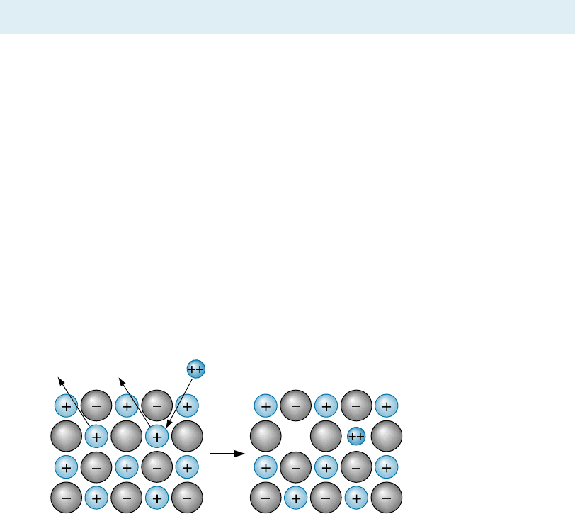
An important substitutional point defect occurs when an ion of one charge replaces
an ion of a di¤erent charge. This might be the case when an ion with a valence of þ2
replaces an ion with a valence of þ1 (Figure 4-3). In this case, an extra positive charge
is introduced into the structure. To maintain a charge balance, a vacancy might be
Figure 4-3
When a divalent cation
replaces a monovalent
cation, a second
monovalent cation must
also be removed, creating
a vacancy.
4-2 Other Point Defects 97
created where a þ1 cation normally would be located. Again, this imperfection is ob-
served in materials that have pronounced ionic bonding.
Thus, in ionic solids, when point defects are introduced the following rules have to
be observed:
(a) a charge balance must be maintained so that the crystalline material as a whole
is electrically neutral;
(b) a mass balance must be maintained; and
(c) the number of crystallographic sites must be conserved.
For example, in nickel oxide (NiO) if one oxygen ion is missing, it creates an oxy-
gen ion vacancy (designated as V
O
€). Each dot (.) on the subscript indicates an e¤ective
positive charge of one. To maintain stoichiometry, mass balance and charge balance we
must also create a vacancy of nickel ion (designated as V
00
Ni
). Each accent (
0
) in the
superscript indicates an e¤ective charge of negative 1.
The Kr
€
oger-Vink notation is used to write the defect chemistry equations.
4-3 Dislocations
Dislocations are line imperfections in an otherwise perfect crystal. They are introduced
typically into the crystal during solidification of the material or when the material
is deformed permanently. Although dislocations are pre sent in all materials, including
ceramics and polymers, they are particularly useful in explaining deformation and
strengthening in metallic materials. We can identify three types of dislocations: the screw
dislocation, the edge dislocation, and the mixed dislocation.
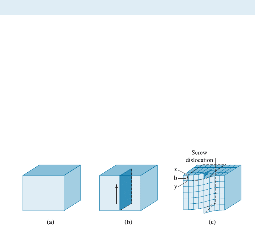
Screw Dislocations The screw dislocation (Figure 4-4) can be illustrated by cutting
partway through a perfect crystal, then skewing the crystal one atom spacing. If we
follow a crystallographic plane one revolution around the axis on which the crystal
was skewed, starting at point x and traveling equal atom spacings in each direction, we
finish one atom spacing below our starting point (point y). The vector required to
complete the loop and return us to our starting point is the Burgers vector b.Ifwe
continued our rotation, we would trace out a spiral path. The axis, or line around
which we trace out this path, is the screw dislocation. The Burgers vector is parallel to
the screw dislocation.
Figure 4-4 The perfect crystal (a) is cut and sheared one atom spacing, (b) and (c). The line
along which shearing occurs is a screw dislocation. A Burgers vector b is required to close a
loop of equal atom spacings around the screw dislocation.
C H A P TE R 4 Imperfections in the Atomic and Ionic Arrangements98
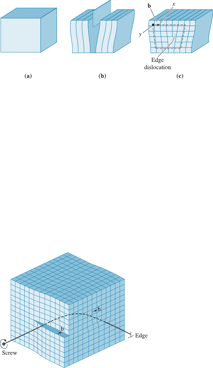
Edge Dislocations An edge dislocation (Figure 4-5) can be illustrated by slicing part-
way through a perfect crystal, spreading the crystal apart, and partly filling the cut with
an extra plane of atoms. The bottom edge of this inserted plane represents the edge
dislocation. If we describe a clockwise loop around the edge dislocation, starting at
point x and going an equal number of atoms spacings in each direction, we finish, at
point y, one atom spacing from the starting point. The vector required to complete the
loop is, again, the Burger s vector. In this case, the Burgers vector is perpendicular to the
dislocation. By introducing the dislocation, the atoms above the dislocation line are
squeezed too closely together, while the atoms below the dislocation are stretched too
far apart. The surrounding region of the crystal has been disturbed by the presence of
the disloc ation. [This is illustrated later on in Figure 4-8(b).] Unlike an edge dislocation,
a screw dislocation cannot be visualized as an extra half plane of atoms.
Mixed Dislocations As shown in Figure 4-6, mixed dislocations have both edge and
screw components, with a transition region between them. The Burgers vector, how-
ever, remains the same for all portions of the mixed dislocation.
Figure 4-5 The perfect crystal in (a) is cut and an extra plane of atoms is inserted (b). The
bottom edge of the extra plane is an edge dislocation (c). A Burgers vector b is required to
close a loop of equal atom spacings around the edge dislocation. (Adapted from J.D.
Verhoeven, Fundamentals of Physical Metallurgy, Wiley, 1975.)
Figure 4-6
A mixed dislocation. The
screw dislocation at the front
face of the crystal gradually
changes to an edge
dislocation at the side of the
crystal. (Adapted from W.T.
Read, Dislocations in
Crystals. McGraw-Hill,
1953.)
4-3 Dislocations 99