Zuo-Guang. Ye Advanced Dielectric Piezoelectric and Ferroelectric Materials: Synthesis, Characterisation and Applications
Подождите немного. Документ загружается.

Handbook of dielectric, piezoelectric and ferroelectric materials740
Usually, the PZT film, especially the thin sol–gel film, tends to crack at
the edge of the bottom electrode. Electric short-circuit occurs when the
patterned top electrode interconnection passes across the edge of the bottom
electrode although this part is often designed to be covered by PZT film.
Therefore, making a good interconnection between the top electrode and its
electric contact pad is one of the challenges in pMUT fabrication. In our
design, a polyimide layer is utilized to cover the top of the PZT film at the
edge part to overcome this problem. Figure 24.14 shows that the smooth
surface and well-curved slope covered at the edge of PZT layer facilitate the
interconnection of the top electrode. In addition, the very dense polyimide
layer prevents the electric short-circuit at the edge part of the bottom electrode.
24.5.3 Etching of the PZT thick film
In general, there are two approaches to micromachine the PZT film: dry
etching and wet etching. Reactive ion etching (RIE), inductively coupled
plasma (ICP) and electron cyclotron resonance (ECR) excitation, have been
reported to etch PZT films. These studies are driven primarily by ferroelectric
memory applications, where the film thickness generally does not exceed
250nm. However, the dry PZT etching technique is not well developed
because there is no common halogenous gas that forms a volatile compound
with all three elements (Pb, Zr, Ti) to guarantee the residue-free removal of
the film. The volatility of the reactive products of individual Pb, Zr and Ti is
different. Heating the substrate or increasing the ion bombardment is often
Polyimide
Active area
Diaphragm
PZT
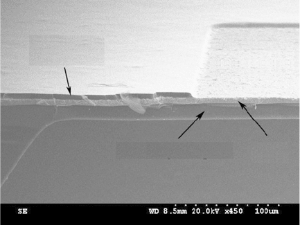
24.13
Top profile image of a fabricated pMUT diaphragm. Backside
silicon is wet etched by the KOH. The PZT film is 5µm in thickness
and the total thickness of the support layer is 13µm. The effective
top electrode area of the element is defined by an opened window
on polyimide layer.
WPNL2204
Piezoelectric thick films for MEMS application 741
a way to obtain a uniform etch of PZT layer. It is very difficult to achieve a
high etch rate of the PZT with adequate etch selectivity to electrode materials
and photoresist mask. As a result, the dry etching technique is too slow to
etch thick composite PZT films with thickness up to 20µm. The wet etching
of PZT films remains the only good choice for thick PZT etching in our
pMUT fabrication.
Since the wet etching process is isotropic, lateral etching cannot be avoided.
We define the active pMUT element with patterned bottom electrode together
with an open window through polyimide layer to avoid the etching of small
lateral PZT patterns. Large ‘V’s are etched on PZT films for the access to
bottom electrode bonding pads. Since this bonding pads area is far away
Polyimide
PZT
Ti/Pt
Polyimide
PZT
(a)
(b)
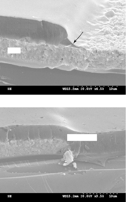
24.14
Polyimide layers on the fabricated pMUT facilitate the electric
interconnection of the top electrode and reduce the parasitic
capacitance. (a) Isolation layer for defining the effective top electrode
area. (b) Polyimide protection layer at the device edge.
WPNL2204
Handbook of dielectric, piezoelectric and ferroelectric materials742
from the active part of the pMUT element, undercutting does not affect the
operation of the pMUT.
In our work, 50ml concentrated HCl (37%), 50 ml water and 0.1ml HF
(48%) were mixed as the etch solution. A 5 µm-thick AZ9260 photoresist
was patterned as an etching mask. The etching process was conducted before
the final annealing of the composite PZT film because the etching is relatively
faster if the PZT film is not fully crystallized. The etch rate at room temperature
was about 0.8µm/min. The whitish metal-fluoride residues formed on the
etch area during PZT film etching were rinsed off by de-ionized (DI) water
after every minute of etching. The residue-free etching of PZT film can be
achieved in few etch–rinse cycles. Figure 24.15 shows an optical image of a
wet etched composite film covered by polyimide layer. It can be seen that the
etching edge is neat and straight at this magnification. However, under etching
as large as 20µm and some profile irregularity can be observed, which
means small etching patterns less than 40 µm are impossible by using wet
etching. Fortunately, for our pMUT design, the achieved wet etching results
are good enough at the device edge which is far away from the pMUT
diaphragm.
24.6 Performances of thick film pMUT
24.6.1 Piezoelectric response and simulated properties of
the fabricated thick film
As a transducer, the pMUT is supposed to work at around its resonance
frequency. Thus the dynamic piezoelectric response of the fabricated pMUT
was investigated. The resonance frequency of a multilayer PZT/silicon
diaphragm is basically determined by the dimension and the mechanical
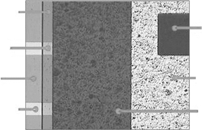
Polyimide/LTO
Polyimide/Pt/LTO
LTO
Pt/LTO
Pt/PZT
Pt/Polyimide/PZT
Polyimide/PZT
24.15
Optical image of the edge part of a fabricated pMUT element.
The wet etched composite film is covered by a transparent polyimide
layer. The etching edge of PZT is clear and straight. The area marked
with Pt/PZT is the active part of a 250 × 250µm
2
pMUT element.
WPNL2204
Piezoelectric thick films for MEMS application 743
properties of the PZT and silicon. As long as the fundamental resonance
frequency of the PZT/silicon diaphragm is measured, the mechanical properties
of the thick PZT film can be extracted based on the ANSYS modal analysis
method.
A fabricated 2 × 2mm
2
pMUT diaphragm was measured and used for
FEA. The measured thicknesses of the PZT film and support layer are 5 µm
and 13µm, respectively, as shown in Fig. 24.13. An external ac electric field
with sweeping frequency was used to excite the vibration of the pMUT and
the vibration velocity at the central point was recorded as the function of the
frequency. Figure 24.16 shows the measured velocity response by using a
Polytec PSV300 scanning laser vibrometer. Only two vibration modes at
41.6 kHz (fundamental mode) and 146.8kHz (sixth mode) were detected.
Assuming the density and Poisson’s ratio of the PZT film are 7500kg/m
3
and
0.25, respectively, the Young’s modulus of the film was determined as 75.2 GPa
when the simulated fundamental resonance frequency equals 41.6kHz. The
bulk silicon material properties used for the simulation and the estimated
mechanical properties of the thick composite film are listed in Table 24.3. In
the FEA simulation, the influence of the thin electrode and SiO
2
layers was
ignored.
After determining the mechanical properties of the composite PZT film,
we further estimated the piezoelectric stress coefficient of the film based on
its quasi-static piezoelectric response. Figure 24.17 shows the quasi-static
piezoelectric displacement at the center of the same pMUT element driven
by a sine wave voltage of 500 Hz, which is much lower than its resonance
frequency. The bias dc voltage is 20 V and the peak-to-peak driving voltage
Velocity (a.u.)
41.6kHz
(1,1)
146.8 kHz
(1,3)
25 50 75 100 125 150 175
Frequency (kHz)
24.16
Frequency response of vibration velocity at central point of a
square 2mm × 2 mm diaphragm driven by 5 µm-thick PZT film. About
13µm-thick support layer was left after DRIE.
WPNL2204
Handbook of dielectric, piezoelectric and ferroelectric materials744
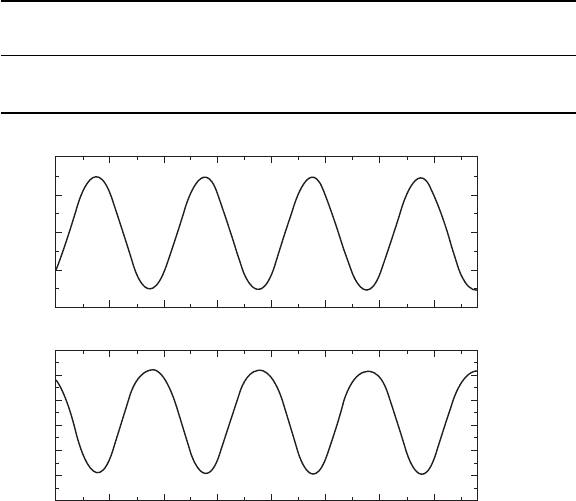
is 30V, resulting in a peak-to-peak center displacement of the PZT/silicon
diaphragm at about 200nm, corresponding to a quasi-static piezoelectric
center displacement/voltage sensitivity of 6.67 nm/V. This deflection/voltage
sensitivity was then used to estimate the piezoelectric stress coefficients of
the composite PZT films. The other materials properties determined by model
analysis shown in Table 24.3 remained unchanged during simulation. The
obtained piezoelectric coefficients e
31
and e
33
of the composite PZT film
were –14.8 and 18.8 C/m
2
, respectively, quite close to those of the bulk PZT
ceramics. The good piezoelectric properties are attributable to the applied dc
bias voltage.
Figure 24.18 shows the displacement magnitude/phase-frequency properties
of the same pMUT around the fundamental resonance frequency. During the
measurement, a dc bias of 20 V was applied to ensure the film has sufficient
polarization. A 30V peak-to-peak ac voltage was superimposed on the dc
bias as a driving voltage. It is seen that in the vicinity of the resonance
Table 24.3
Estimated mechanical properties of PZT film from mode
analysis and material properties of silicon used in simulation
Materials Young’s modulus Poisson’s ratio Density
(GPa) (kg/m
3
)
PZT 75.2 0.25 7500
Silicon 150 0.17 2330
2×2mm
2
, 20V
Bias
, 30V
PP
Driving volttage (V)
Displacement (nm)
40
30
20
10
0
150
100
50
0
–50
–100
–150
01 23 456 7
Time (ms)
24.17
Quasi-static piezoelectric center displacement of the 2 × 2mm
2
diaphragm measured at 500Hz for estimation of piezoelectric
properties of the thick PZT film.
WPNL2204
Piezoelectric thick films for MEMS application 745
frequency, the deflection amplitude of the central point of the diaphragm
reaches about 2.8 µm, and the phase shifts about 180°. The fundamental
vibration mode is the interested mode which can be utilized as both ultrasound
transmitters and receivers.
24.6.2 Output sound pressure level
23,24
The performance of the pMUT as an ultrasound transmitter can be evaluated
by output sound pressure level (SPL), which is expressed by
SPL = 20 log
rms
ref
P
P
24.1
where P
rms
is the output sound pressure at the measuring point which should
be far away from the transmitter, P
ref
is reference sound pressure and equals
2 × 10
–5
Pa.
The continuous ultrasound wave emitted by the transmitter is measured in
air with Brüel and Kjær 2825 test system, including a 7521 signal analyzer
interface module, 3016 input module, and 2670 microphone. The highest
frequency of the system can reach 100kHz. The output SPL of the same
transmitter as shown in Fig. 24.18 is measured at the same driving conditions.
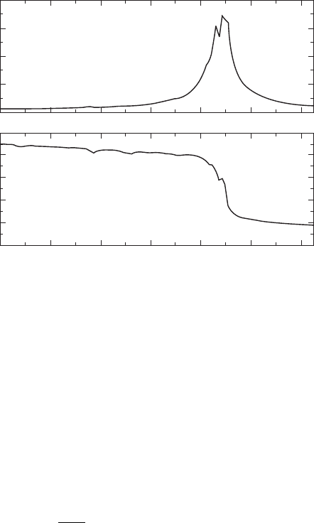
Figure 24.19(a) shows the test result. The distance between the transmitter
and the microphone is 12 mm. In comparison with Fig. 24.18, Fig. 24.19(a)
indicates that the output SPL of a pMUT also reaches its maximum at the
resonance frequency. The output SPL is 107.8dB at 41.3 kHz. Among the
20 25 30 35 40 45 50
Frequency (kHz)
2 × 2mm
2
Bias 20V, 30V
PP
8 nm/mV 41.53 kHz
42.15 kHz
Magnitude (mV)
400
300
200
100
0
Phase (degree)
180
120
60
0
–60
–120
24.18
Frequency spectra of magnitude/phase of the 2 × 2mm
2
diaphragm at around fundamental resonance frequency.
WPNL2204
Handbook of dielectric, piezoelectric and ferroelectric materials746
fabricated pMUTs, the highest SPL obtained is around 120dB at a distance
of 12mm. Figure 24.19(b) shows another example. The SPL is 116.8 dB at
76.3kHz for a square pMUT element with side length of 1.5mm. As a
ultrasonic transmitter, this output SPL is quite good.
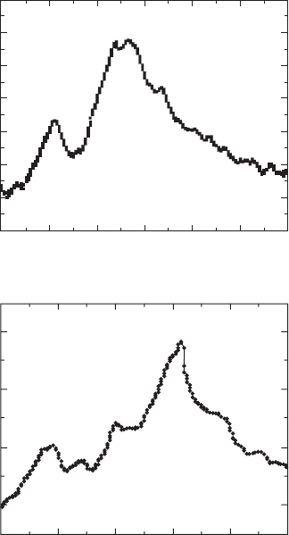
We also investigated the effect of the dc bias, the driving voltage and the
measuring distance on the output SPL and resonance frequency of a pMUT
with 7µm-thick composite PZT layer. Figure 24.20 shows the results. The
output SPL increases with the increase of the applied dc bias and saturated
at certain dc bias level (30 V as shown in Fig. 24.20a) at which the polarization
of the film approaches saturation. Figure 24.20(b) shows that the output SPL
increases with the driving voltage and decreases with the increase of the
measuring distance.
41.3kHz, 107.8 dB
20V dc bias, 30 V
P-P
36 38 40 42 44 46 48
Frequency (kHz)
(a)
Sound pressure level (dB)
120
110
100
90
80
70
60
50
76.3 kHz, 116.8 dB
20 V dc bias, 20 V
P-P
70 72 74 76 78 80
Frequency (kHz)
(b)
Sound pressure level (dB)
120
100
80
60
24.19
Frequency dependence of output sound pressure level of
pMUTs with different diaphragm sizes: (a) 2 mm × 2mm, (b)1.5 mm
× 1.5 mm.
WPNL2204
Piezoelectric thick films for MEMS application 747
24.6.3 Directivity of 2D pMUT array
25
The pMUT array has potential applications in object detection and
environmental recognition, either at low ultrasonic frequency in air or at
high frequency in liquid medium or human body. In the design of pMUT
array for these applications, the number of elements in the array has to be
increased to meet the requirement of the resolution and signal to noise ratio.
As a result, the whole array will occupy a large area on the silicon wafer. In
this case, it would be increasingly difficult to maintain uniform thickness of
the diaphragm throughout a whole array by wet silicon etching. This problem
can be solved by making use of SOI wafers and DRIE etching since the
Sound pressure level (dB)
114
112
110
108
106
104
102
100
98
10 20 30 40 50 60
bias (V)
(a)
30 V
p–p
, 12mm
Thick R-A
PZT 7 µm
2 mm × 2mm
Driving voltage (V)
0 10 2030405060
Bias 30 V, 12 mm
Bias 30 V, 30 V
p-p
Thick R-A
0 50 100 150 200 250
Distance (mm)
(b)
Sound pressure level (dB)
120
116
112
108
104
100
96
92
88
24.20
Output sound pressure level at resonance frequency versus (a)
dc bias (at driving voltage of 30 V
p-p
), (b) peak to peak driving
voltage (at dc bias of 30V) and distance between measuring point
and transmitter (bias 30V, 30 Vp-p).
WPNL2204
Handbook of dielectric, piezoelectric and ferroelectric materials748
etching will stop automatically at the SiO
2
layer and the diaphragm thickness
will be determined by the device layer of the SOI wafer. This can ensure a
very uniform diaphragm thickness over the whole wafer, resulting in a uniform
resonance frequency of the individual elements of pMUT array. Figure 24.21
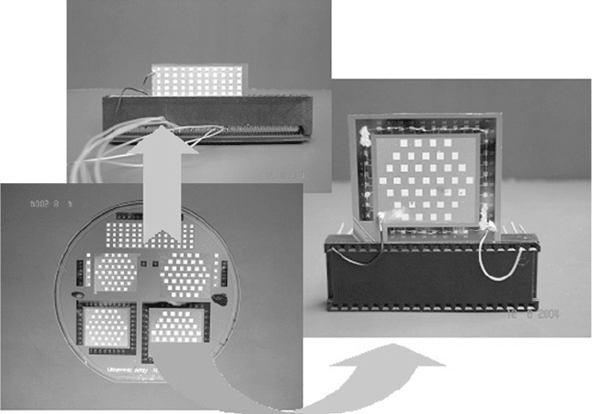
shows fabricated pMUT arrays on a 4-inch (100 mm) SOI wafer for ultrasound
beam forming and beam steering applications. The individual devices were
separated by wafer dicing and electrically connected by wire bonding.
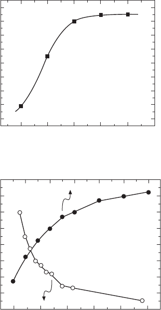
We investigated the directivity of the ultrasound beam emitted by the
pMUT array at resonance frequency. The tested array consists of 37 elements
with a size of 1.5 × 1.5 mm
2
. An ac driving voltage of 10 V
p-p
superimposed
on a dc bias of 30V is applied across the 6µm-thick piezoelectric layer. The
support silicon layer is 40 µm thick. The array surface is rotated from –90°
to +90° with respect to the normal direction of an acousto-optic sensor. The
displacement output of the sensor in response to the radiated ultrasound
from the array was recorded at every rotation step of 1° and was utilized as
the measure of sound pressure. The ultrasound radiation pattern of the array
measured at its resonant frequency of 160 kHz is shown in Fig. 24.22. It can
be seen that the main lobe is very sharp and tall, which reveals that the
fabricated transmitter array can be employed in beam forming and beam
steering applications.
24.21
Piezoelectric ultrasonic transmitter arrays fabricated on a 4-inch
(100 mm) silicon wafer and a separate array device after wafer dicing
and wire bonding.
WPNL2204

Piezoelectric thick films for MEMS application 749
24.6.4 Electromechanical coupling coefficient
The effective electromechanical coupling coefficient k
2
of pMUT is defined as
k
2
= 1 – (f
r
/f
a
)
2
24.2
where f
r
means the resonance frequency and f
a
the anti-resonance frequency
in an impedance frequency spectrum, respectively.
Figure 24.23 shows the measurement results of the impedance and phase
frequency spectrum for a 0.5 × 0.5mm
2
pMUT element with a 7µm-thick
PZT film and 10µm-thick support layer. The impedance frequency spectrum
of the pMUT was characterized using an Agilent 4294A Precision Impedance
Analyzer. The measured f
r
and f
a
are 259.87 and 261.73 kHz, respectively,
resulting in a coupling coefficient of 1.42% as calculated according to equation
(24.2). The measured value is similar to that of a diaphragm prepared with
sol–gel PZT film.
26
With optimum thicknesses of PZT and silicon in the
diaphragm, a better coupling coefficient can be expected by using our thick
composite PZT film.
24.6.5 Equivalent circuit parameters of the pMUT
The Q factor of the pMUT can be determined by the real part of the impedance
frequency spectrum, which is defined as Q = f
r
/∆f, where the resonance
frequency f
r
is the frequency at which the real part of the impedance reaches
its maximum, ∆f is the width of the peak at its half height, so-called 3dB
Displacement (nm)
2.5
2.0
1.5
1.0
0.5
0.0
0.5
1.0
1.5
2.0
2.5
180
150
120
90
60
30
0
330
300
270
240
210
24.22
The directivity pattern of a pMUT array fabricated with SOI
wafer and measured by using a diaphragm type acousto-optic
sensor.
WPNL2204