Tsoulfanidis N. Measurement and detection of radiation
Подождите немного. Документ загружается.

248
MEASUREMENT
AND
DETECTION
OF
RADIATION
10"
lol=
10" 1014
Impurity concentration, at/cm3
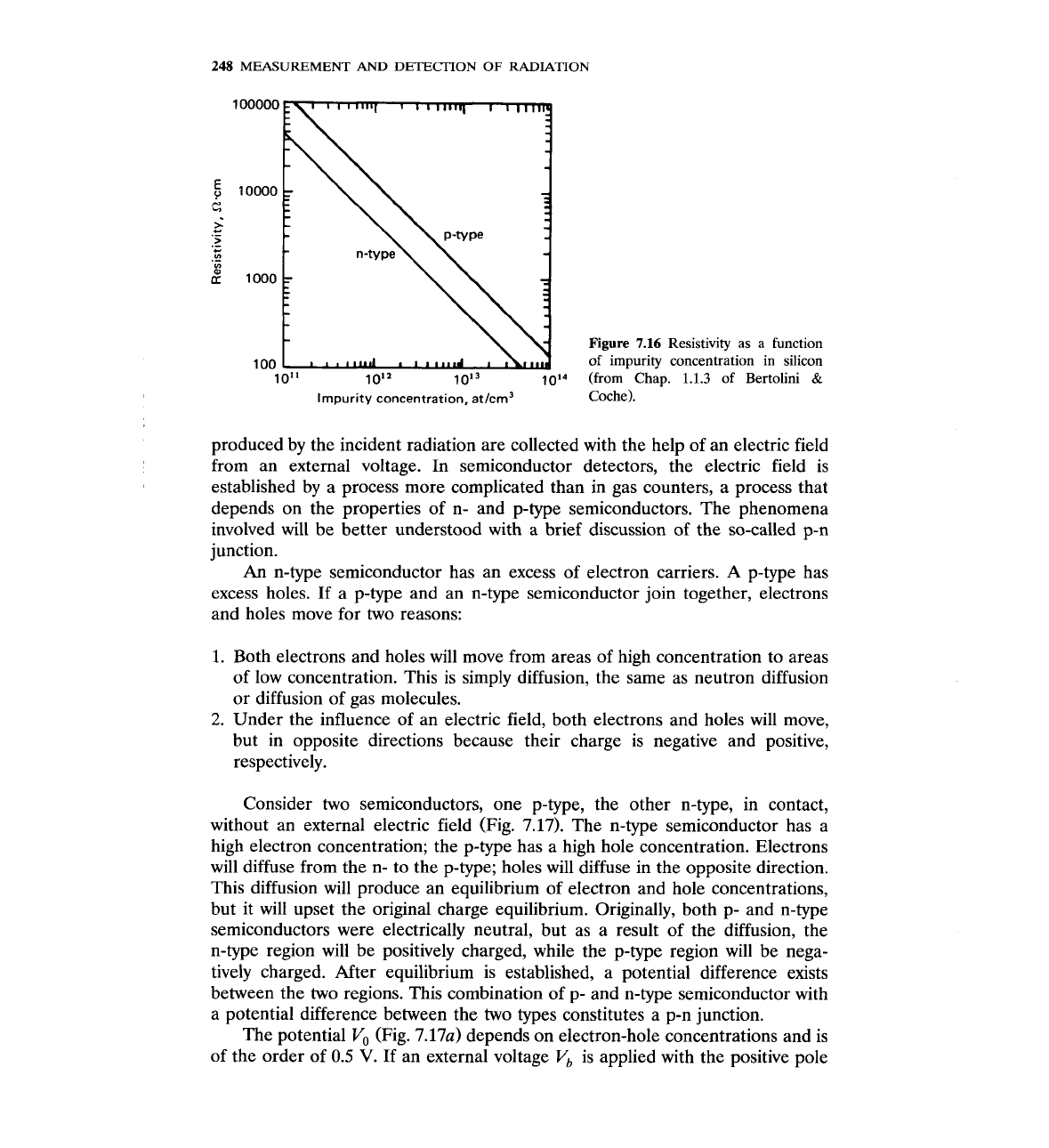
Figure
7.16
Resistivity as a function
of impurity concentration in silicon
(from Chap.
1.1.3
of Bertolini
&
Coche).
produced by the incident radiation are collected with the help of an electric field
from an external voltage. In semiconductor detectors, the electric field is
established by a process more complicated than in gas counters, a process that
depends on the properties of n- and p-type semiconductors. The phenomena
involved will be better understood with a brief discussion of the so-called
p-n
junction.
An
n-type semiconductor has an excess of electron carriers.
A
p-type has
excess holes. If a p-type and an n-type semiconductor join together, electrons
and holes move for two reasons:
1.
Both electrons and holes will move from areas of high concentration to areas
of low concentration. This is simply diffusion, the same as neutron diffusion
or diffusion of gas molecules.
2.
Under the influence of an electric field, both electrons and holes will move,
but in opposite directions because their charge is negative and positive,
respectively.
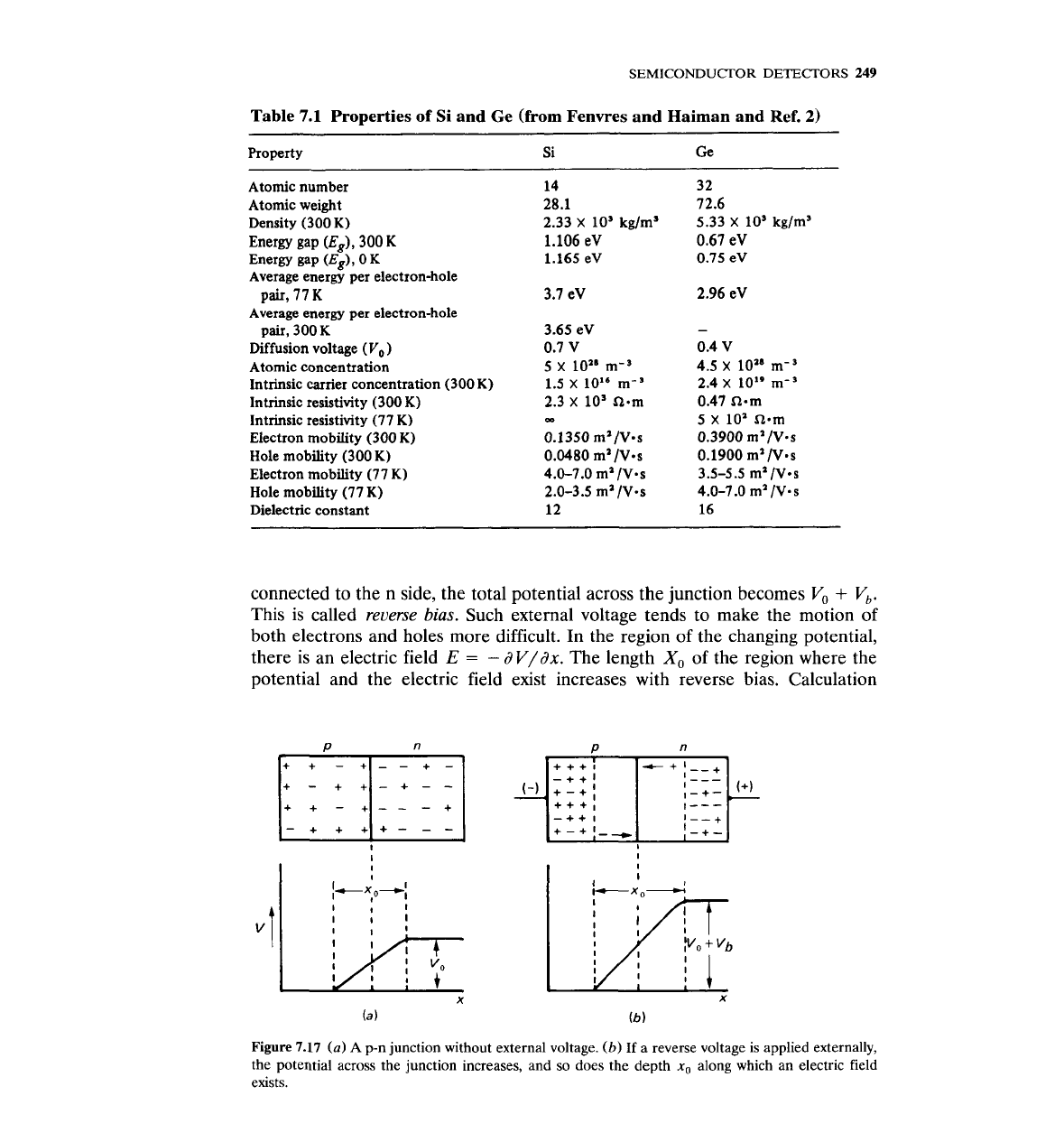
Consider two semiconductors, one p-type, the other n-type, in contact,
without an external electric field (Fig. 7.17). The n-type semiconductor has a
high electron concentration; the p-type has a high hole concentration. Electrons
will diffuse from the n- to the p-type; holes will diffuse in the opposite direction.
This diffusion will produce an equilibrium of electron and hole concentrations,
but it will upset the original charge equilibrium. Originally, both p- and n-type
semiconductors were electrically neutral, but as a result of the diffusion, the
n-type region will be positively charged, while the p-type region will be nega-
tively charged. After equilibrium is established, a potential difference exists
between the two regions. This combination of p- and n-type semiconductor with
a potential difference between the two types constitutes a p-n junction.
The potential
V,
(Fig. 7.17~) depends on electron-hole concentrations and is
of the order of
0.5
V.
If an external voltage
Vb
is applied with the positive pole
SEMICONDUCTOR DETECTORS
249
Table
7.1
Properties of Si and Ge (from Fenvres and Haiman and Ref.
2)
Property Si Ge
Atomic number 14 3 2
Atomic weight 28.1 72.6
Density (300 K)
2.33
x
lo3
kg/mS
5.33
X
lo3
kg/m3
Energy gap
(E8),
300
K
1.106 eV 0.67 eV
Energy gap
(Eg),
0
K
1.165 eV 0.75 eV
Average energy per electron-hole
pair, 77
K
3.7 eV 2.96 eV
Average energy per electron-hole
pair, 300 K 3.65 eV
-
Diffusion voltage
(V,)
0.7 V 0.4 V
Atomic concentration 5
x
10aB
m-'
4.5
X
rn-)
Intrinsic carrier concentration (300 K)
1.5
X
1016 m-3
2.4
X
10" m-3
Intrinsic resistivity
(300
K)
2.3
x
10' f2.m 0.47 a-m
Intrinsic resistivity (77 K)
OD
5
X
10' i2.m
Electron mobility (300 K) 0.1350 m"V.s
0.3900 ml/V.s
Hole mobility (300 K)
0.0480 ma/V.s 0.1900 ma/V.s
Electron mobility (77 K)
4.0-7.0 m"V-s 3.5-5.5 m1 1V.s
Hole mobility (77 K)
2.0-3.5 ma/V.s 4.0-7.0 ma/V.s
Dielectric constant
12
16
connected to the n side, the total potential across the junction becomes
Vo
+
Vb.
This is called
reverse bias.
Such external voltage tends to make the motion of
both electrons and holes more difficult. In the region of the changing potential,
there is an electric field
E
=
-
dV/dx.
The length
Xo
of the region where the
potential and the electric field exist increases with reverse bias. Calculation
Figure
7.17
(a) A
p-n junction without external voltage.
(b)
If a reverse voltage is applied externally,
the potential across the junction increases, and so does the depth
x,
along which an electric field
exists.
250
MEASUREMENT
AND
DETECTION OF RADIATION
shows that
Xo
db
p(VO
+
Vb) for p-type semiconductor (7.11~)
and
x0
=
41%
p(Vo
+
Vb)
for n-type semiconductor
(7.11 b)
where
p(f2
-
m) is the resistivity of the crystal. Application of a negative
potential on the n side will have the opposite effect. The total potential
difference will be
Vo
-
Vb. This is called forward bias. For a successful detector,
reverse bias is applied. Since, usually,
Vb
s
Vo, Xo
-
K.
In practice, a p-n junction is not made by bringing two pieces of semicon-
ductor into contact. Instead, one starts with a semiconductor of one type (say,
n-type) and then transforms one end of it into the other type (p-type).
7.4.2
The p-n Junction Operating as a Detector
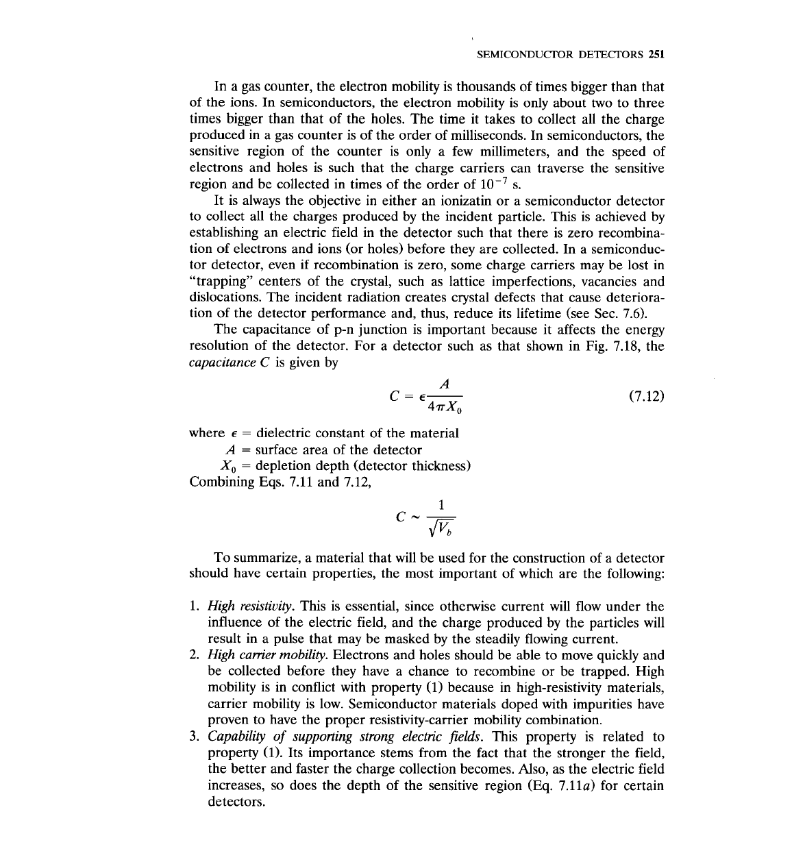
The operation of a semiconductor detector is based, essentially, on the proper-
ties of the p-n junction with reverse bias (Fig. 7.18). Radiation incident upon the
junction produces electron-hole pairs as it passes through it. For example,
if
a
5-MeV alpha particle impinges upon the detector and deposits all its energy
there, it will create about
5
x
lo6
eV
-
1.7
x
lo6
electron-hole pairs
3
eV/pair
Electrons and holes are swept away under the influence of the electric field and,
with proper electronics, the charge collected produces a pulse that can be
recorded.
The performance of a semiconductor detector depends on the region of the
p-n junction where the electric field exists (region of width
Xo, Fig. 7.18).
Electrons and holes produced in that region find themselves in an environment
similar to what electrons and ions see in a plate ionization chamber (see
Sec.
5.4).
There are some differences, however, between these two types of detectors.
SEMICONDUCTOR
DETECTORS
251
In a gas counter, the electron mobility is thousands of times bigger than that
of the ions. In semiconductors, the electron mobility is only about two to three
times bigger than that of the holes. The time it takes to collect all the charge
produced in a gas counter is of the order of milliseconds. In semiconductors, the
sensitive region of the counter is only a few millimeters, and the speed of
electrons and holes is such that the charge carriers can traverse the sensitive
region and be collected in times of the order of
lop7
s.
It is always the objective in either an ionizatin or a semiconductor detector
to collect all the charges produced by the incident particle. This is achieved by
establishing an electric field in the detector such that there is zero recombina-
tion of electrons and ions (or holes) before they are collected. In a semiconduc-
tor detector, even if recombination is zero, some charge carriers may be lost in
"trapping7' centers of the crystal, such as lattice imperfections, vacancies and
dislocations. The incident radiation creates crystal defects that cause deteriora-
tion of the detector performance and, thus, reduce its lifetime (see Sec.
7.6).
The capacitance of p-n junction is important because it affects the energy
resolution of the detector. For a detector such as that shown in Fig. 7.18, the
capacitance
C
is given by
where
E
=
dielectric constant of the material
A
=
surface area of the detector
X,
=
depletion depth (detector thickness)
Combining Eqs. 7.11 and 7.12,
To summarize, a material that will be used for the construction of a detector
should have certain properties, the most important of which are the following:
1.
High resistivity.
This is essential, since otherwise current will flow under the
influence of the electric field, and the charge produced by the particles will
result in a pulse that may be masked by the steadily flowing current.
2.
High carrier mobility.
Electrons and holes should be able to move quickly and
be collected before they have a chance to recombine or be trapped. High
mobility is in conflict with property (1) because in high-resistivity materials,
carrier mobility is low. Semiconductor materials doped with impurities have
proven to have the proper resistivity-carrier mobility combination.
3.
Capability of supporting strong electric fields.
This property is related to
property
(1).
Its importance stems from the fact that the stronger the field,
the better and faster the charge collection becomes. Also, as the electric field
increases, so does the depth of the sensitive region (Eq. 7.11a) for certain
detectors.
252
MEASUREMENT
AND
DETECTION
OF
RADIATION
4. Perfect crystal lattice.
Apart from externally injected impurities, the semicon-
ductor detector material should consist of a perfect crystal lattice without any
defects, missing atoms, or interstitial atoms. Any such defect may act as a
"trap" for the moving charges.
7.5 THE DIFFERENT TYPES OF SEMICONDUCTOR DETECTORS
The several types of semiconductor detectors that exist today differ from one
another because of the material used for their construction or the method by
which that material is treated. The rest of this section describes briefly the
method of construction and the characteristics of the most successful detectors
-made of silicon or germanium-and two promising ones made of
CdTe and
Hgb
7.5.1
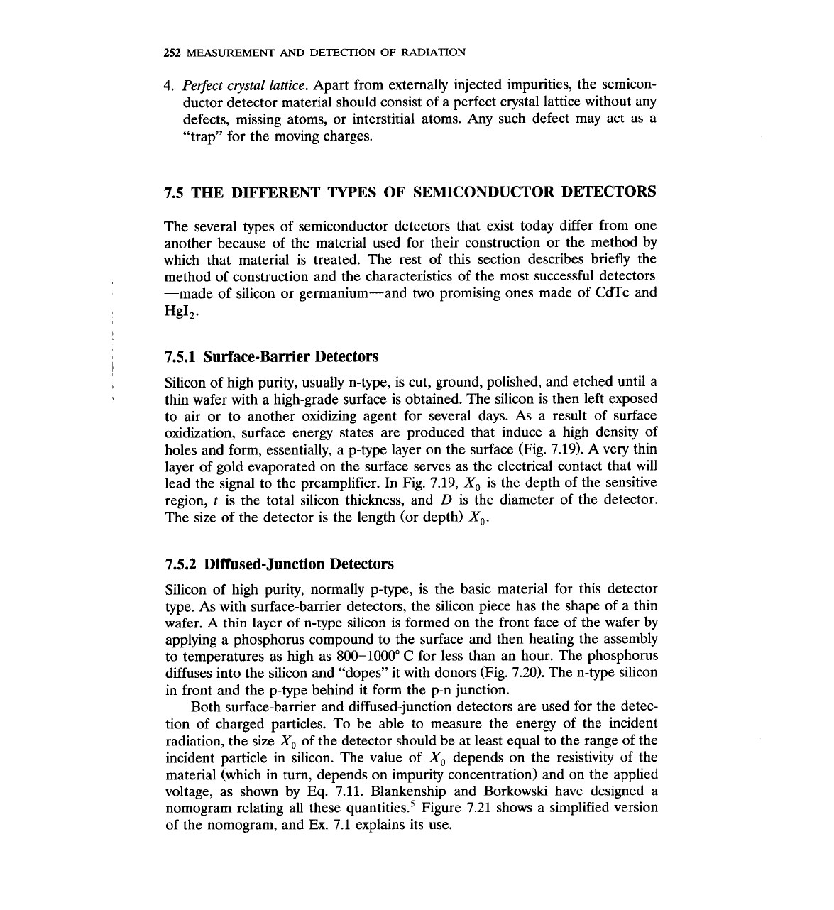
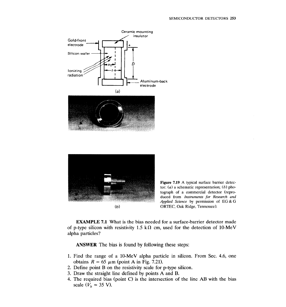
Surface-Barrier Detectors
Silicon of high purity, usually n-type, is cut, ground, polished, and etched until a
thin wafer with a high-grade surface is obtained. The silicon is then left exposed
to air or to another oxidizing agent for several days. As a result of surface
oxidization, surface energy states are produced that induce a high density of
holes and form, essentially, a p-type layer on the surface (Fig. 7.19).
A
very thin
layer of gold evaporated on the surface serves as the electrical contact that will
lead the signal to the preamplifier. In Fig. 7.19,
X,,
is the depth of the sensitive
region,
t
is the total silicon thickness, and
D
is the diameter of the detector.
The size of the detector is the length (or depth)
Xo.
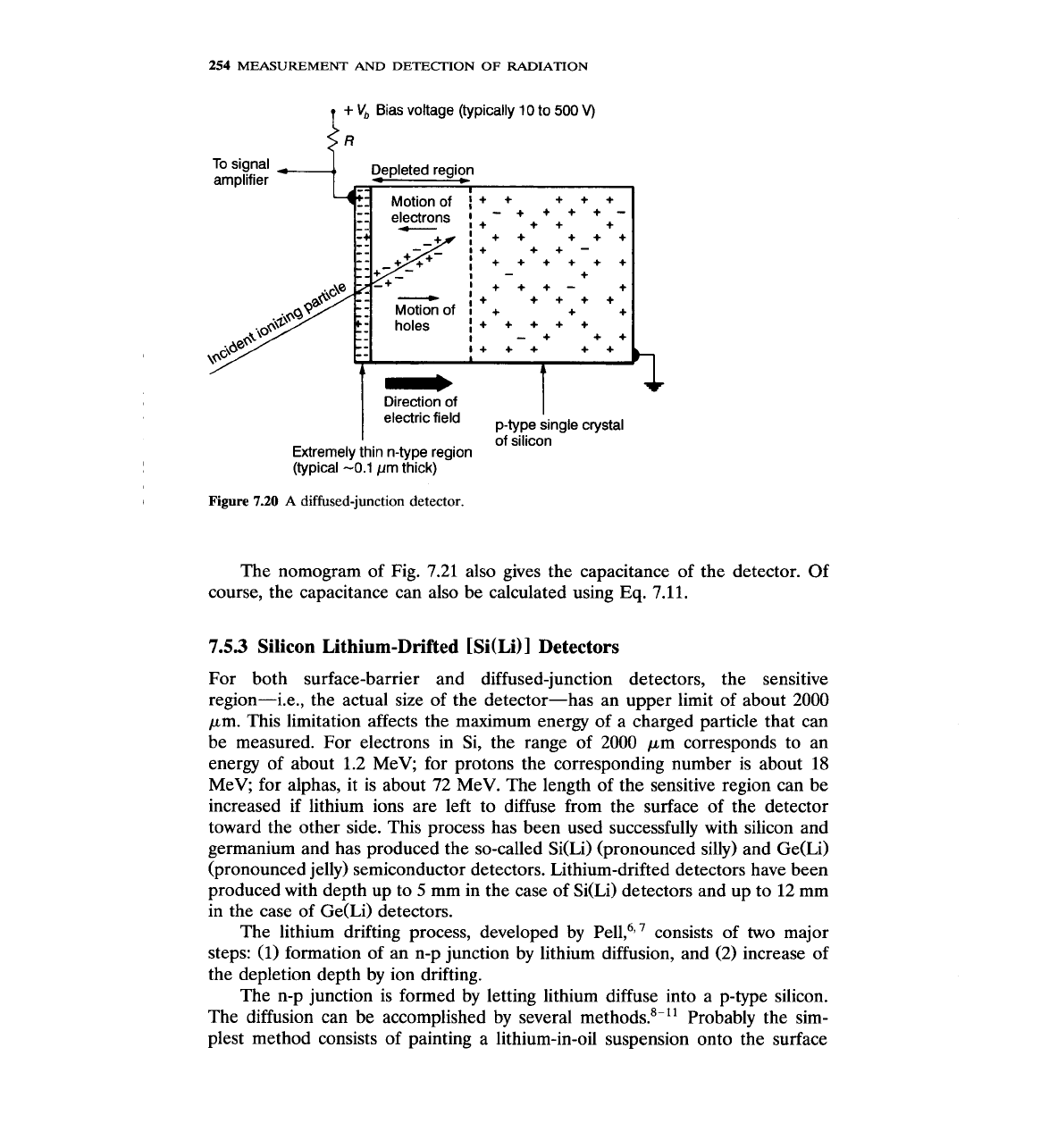
7.5.2 Diffused-Junction Detectors
Silicon of high purity, normally p-type, is the basic material for this detector
type. As with surface-barrier detectors, the silicon piece has the shape of a thin
wafer.
A
thin layer of n-type silicon is formed on the front face of the wafer by
applying a phosphorus compound to the surface and then heating the assembly
to temperatures as high as 800-1000" C for less than an hour. The phosphorus
diffuses into the silicon and "dopes" it with donors (Fig. 7.20). The n-type silicon
in front and the p-type behind it form the p-n junction.
Both surface-barrier and diffused-junction detectors are used for the detec-
tion of charged particles. To be able to measure the energy of the incident
radiation, the size
Xo
of the detector should be at least equal to the range of the
incident particle in silicon. The value of
X,,
depends on the resistivity of the
material (which in turn, depends on impurity concentration) and on the applied
voltage, as shown by Eq. 7.11. Blankenship and Borkowski have designed a
nomogram relating all these
q~antities.~ Figure 7.21 shows a simplified version
of the nomogram, and Ex. 7.1 explains its use.
Ceramic mounting
/
insulator
Gold-front
electrode
Silicon wafer
Ionizing
t
radiation
I
.
Aluminum-back
electrode
(b)
ORTEC,
Oak
Ridge, Tennessee).
EXAMPLE
7.1
What is the bias needed for a surface-barrier detector made
of p-type silicon with resistivity
1.5
kR
cm, used for the detection of 10-MeV
alpha particles?
ANSWER
The bias is found by following these steps:
Find the range of a 10-MeV alpha particle in silicon. From Sec.
4.6,
one
obtains
R
=
65
pm (point
A
in Fig. 7.21).
Define point
B
on the resistivity scale for p-type silicon.
Draw the straight line defined
by
points
A
and
B.
The required bias (point
C)
is the intersection of the line
AB
with the bias
scale
(Vb
-3
35
V).
254
MEASUREMENT AND
DETECTION
OF
RADIATION
+
V,
Bias voltage (typically 10 to 500
V)
IR
To signal
+
+
+
+
++-
++++++
+
I+++-
&GX-+-
1
+
++++
+
--
.'on of
7
holes
++:-+;++:++:
4
+
+
-
Direction of
I
field
p-type single crystal
of silicon
Extremely thin n-type region
(typical -0.1 pm thick)
Figure
7.20
A
diffused-junction detector.
The nomogram of Fig. 7.21 also gives the capacitance of the detector. Of
course, the capacitance can also be calculated using
Eq.
7.11.
7.5.3
Silicon Lithium-Drifted [Si(Li)l Detectors
For both surface-barrier and diffused-junction detectors, the sensitive
region-i.e., the actual size of the detector-has an upper limit of about 2000
pm. This limitation affects the maximum energy of a charged particle that can
be measured. For electrons in Si, the range of 2000
pm corresponds to an
energy of about 1.2 MeV; for protons the corresponding number is about
18
MeV; for alphas, it is about 72 MeV. The length of the sensitive region can be
increased if lithium ions are left to diffuse from the surface of the detector
toward the other side. This process has been used successfully with silicon and
germanium and has produced the so-called Si(Li) (pronounced silly) and Ge(Li)
(pronounced jelly) semiconductor detectors. Lithium-drifted detectors have been
produced with depth up to
5
mm in the case of Si(Li) detectors and up to 12 mm
in the case of Ge(Li) detectors.
The lithium drifting process, developed by Pe11,6,7 consists of two major
steps: (1) formation of an n-p junction by lithium diffusion, and (2) increase of
the depletion depth by ion drifting.
The n-p junction is formed by letting lithium diffuse into a p-type silicon.
The diffusion can be accomplished by several Probably the sim-
plest method consists of painting a lithium-in-oil suspension onto the surface
SEMICONDUCTOR DETECTORS
255
Snllcon
reslstwty
n
Type
PTVP~
lohm
cml
lohm
cml
+
Detector
bias
IVI
Figure
7.21
The Blankenship and ~orkowski~ nomogram that relates resistivity, detector thickness,
and detector bias. The detector capacitance as a function of detector thickness is also given.

256
MEASUREMENT
AND
DETECTION
OF
RADIATION
I
I
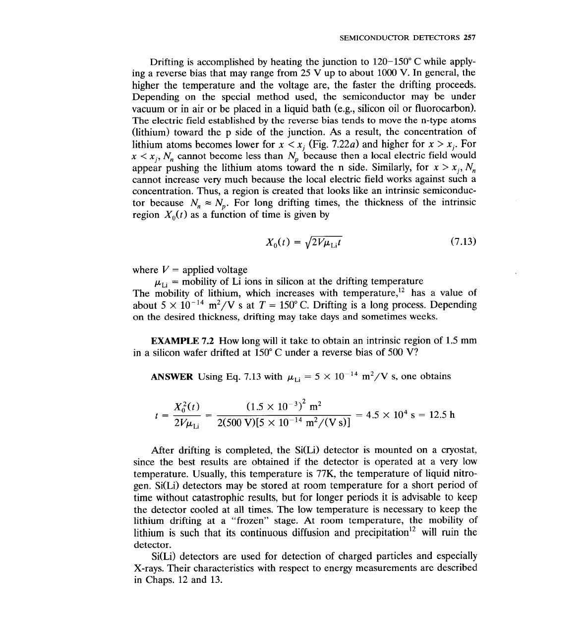
Figure 7.22
(a)
During the diffusion of lithium,
-xo*
I
the donor concentration changes with depth as
I
I
I
I
\
shown.
(b)
During drifting (at elevated tempera-
Xi
ture and under reverse bias), and almost intrinsic
(b)
region is formed with thickness
x,.
from which drifting is to begin. Other methods are lithium deposition under
vacuum, or electrodeposition. After the lithium is applied on the surface, the
silicon wafer is heated at 250-400"
C
for 3-10 min in an inert atmosphere, such
as argon or helium.
Lithium is an n-type impurity (donor atom) with high mobility in silicon (and
germanium; see next section). When the diffusion begins, the acceptor concen-
tration
(N,)
is constant throughout the silicon crystal (Fig. 7.22a), while the
donor concentration
(N,)
is high on the surface and zero everywhere else.
As
the diffusion proceeds, the donor concentration changes with depth, as shown in
Fig. 7.22~. At the depth
xi
where
and n-p junction has been formed (Fig. 7.22b).
After the diffusion is completed, the crystal is left to cool, the excess lithium
is removed, and ohmic contacts are put on the n and p sides of the junction. The
contact on the p side is usually formed by evaporating aluminum or gold doped
with boron. The contact on the n side can be formed by using pure gold or
antimony-doped gold.
SEMICONDUCTOR
DETECTORS
257
Drifting is accomplished by heating the junction to 120-150"
C
while apply-
ing a reverse bias that may range from 25
V
up to about 1000
V.
In general, the
higher the temperature and the voltage are, the faster the drifting proceeds.
Depending on the special method used, the semiconductor may be under
vacuum or in air or be placed in a liquid bath (e.g., silicon oil or fluorocarbon).
The electric field established by the reverse bias tends to move the n-type atoms
(lithium) toward the p side of the junction. As a result, the concentration of
lithium atoms becomes lower for
x
<
xj
(Fig. 7.22~) and higher for
x
>
xj.
For
x
<
xj,
Nn
cannot become less than
N,
because then a local electric field would
appear pushing the lithium atoms toward the n side. Similarly, for
x
>
xj,
Nn
cannot increase very much because the local electric field works against such a
concentration. Thus, a region is created that looks like an intrinsic semiconduc-
tor because
Nn
=
N,,.
For long drifting times, the thickness of the intrinsic
region Xo(t) as a function of time is given by
where
V
=
applied voltage
pLi
=
mobility of Li ions in silicon at the drifting temperature
The mobility of lithium, which increases with temperature,12 has a value of
about 5
X
10-l4
m2/v s at
T
=
150°C. Drifting is a long process. Depending
on the desired thickness, drifting may take days and sometimes weeks.
EXAMPLE
7.2
How long will it take to obtain an intrinsic region of 1.5 mm
in a silicon wafer drifted at 150" C under a reverse bias of 500
V?
ANSWER
Using Eq. 7.13 with
pLi
=
5
X
10-l4 m2/V s, one obtains
After drifting is completed, the Si(Li) detector is mounted on a cryostat,
since the best results are obtained if the detector is operated at a very low
temperature. Usually, this temperature is
77K,
the temperature of liquid nitro-
gen. Si(Li) detectors may be stored at room temperature for a short period of
time without catastrophic results, but for longer periods it is advisable to keep
the detector cooled at all times. The low temperature is necessary to keep the
lithium drifting at a "frozen" stage. At room temperature, the mobility of
lithium is such that its continuous diffusion and
precipitation12 will ruin the
detector.
Si(Li) detectors are used for detection of charged particles and especially
X-rays. Their characteristics with respect to energy measurements are described
in Chaps. 12 and 13.