Seminario J.M. Molecular and Nano Electronics. Analysis, Design and Simulation
Подождите немного. Документ загружается.

134 Yuefei Ma and Jorge M. Seminario
(c)
(a) (b)
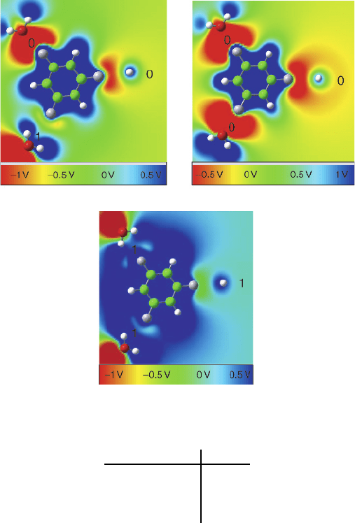
Figure 34 The implementation of a logical AND using a tri-flourobenzene molecule [15]
Input 1 Input 2 Output
111
100
010
000
Figure 35 Truth table of the molecular system shown in Figure 34 [15]
6. Conclusion and perspectives
Both AM and FM can be used to transmit information in molecular wires using molecular
vibrations with a power dissipation of ∼50 nW when working at 1 Tbps.
These kinds of vibrational movements are at the range of terahertz. The vibrational
modes can not only be excited by an electromagnetic wave, but also be detected using
infrared (IR) spectroscopy or Raman spectroscopy if their movements cause changes in
electrostatic dipole (IR active) or in polarizability (Raman active).
When the signal is transferred using molecular vibrational modes, the atoms vibrate
to a certain position, which may introduce a change in the MEP distribution of the
whole molecular system and this change is subsequently transferred through vibronics.
Analysis of programmable molecular electronic systems 135
Thus, by proper programming, the hundreds of molecules inside the nanoCell can be
viewed as signal processing devices.
If information is transmitted using vibronics, the power dissipation could be evaluated
from the energy that excites and keeps the molecular wire to vibrate although you do not
need energy for a molecule to vibrate in its stationary states; molecules vibrate even at
0 K. Our simulation shows that the molecular wire dissipates 0.321 eV for transmitting
one bit data using FM or 0293 eV using AM. If the molecular wire transmits at 1 Tbps,
the molecular wire will dissipate 51 nW using FM or 47 nW using AM, respectively.
Interestingly, the energy needed to excite the molecule with the two inputs is less
than 0.5 eV. This implies that it may be possible to operate 200 millions of these
gates at 10 GHz frequency with just less than 1 W. More precisely, 2 ×10
8
gates ×
10
10
operation/s ×05eV/gate-operation ×16×10
9
J/eV =016 J/s =016 W.
This is certainly a rough estimate, most likely within the same order of magnitude
of the exact value. This estimation considers the energy to change states of the gate
and the energy to excite their inputs. As gates are directly interconnected, losses in
interconnections are perhaps a small fraction of the energy to change states. Nevertheless,
even an error of one or two orders of magnitude underestimating the power consumption
still represents an excellent result. Using a similar logic to calculate the power needed
in the modern Pentium XE, assuming a gate capacitance of 40 aF, amazingly yields
125 W (most likely a lucky match) to which we need to add the energy dissipation
in the interconnects, the energy needed to change the input states, and the utilization
factor among others; all these should account for the total 130 W dissipation in the
microprocessor.
The research work presented in this chapter focuses on the analysis of programmable
molecular arrays, including electrical characterization of a nanoCell device, study of
electron transport in discontinuous thin metal film as well as implementing molecu-
lar vibrational modes and molecular electrostatic potential as methods to process and
transfer information using programmable molecular arrays. This research represents a
major contribution to an in-depth investigation of the implementation of programmable
molecular arrays.
First, the limitations by conventional silicon-based microelectronics in device fabri-
cation and solid-state physics are outlined. New techniques such as single molecular
electronic device, programmable molecular array, etc. are described that may help to
overcome those limitations.
The electrical characteristics of programmable molecular array are thoroughly stud-
ied. The distinct features of programmable molecular array include the memory and
switching phenomena and start-up transitional behavior. Effects of deposition of dif-
ferent molecules are investigated. It is found that the OPE molecules interlinking the
gold islands do not contribute significantly to the electrical conductance. However,
the alkane molecules create additional barrier for the electron transport through the
islands. A programming procedure for the multi-leads molecular array is proposed. In
this method, a matrix of truth valued between each pair of the leads is obtained and
followed by a set of voltage pulses to program the molecular array.
Since the OPE molecules are found not to contribute significantly to the electrical
conductance of the programmable molecular array, it is obvious that the discontinuous
gold film is the fundamental conductor. After reviews of several theoretical models that
explain the electrical conductance through a discontinuous metallic film, a model based
136 Yuefei Ma and Jorge M. Seminario
on the clustering effect of gold atoms is proposed to account for the electrical behavior
of discontinuous gold film in high electrical field. At low field, however, electrons have
not overcome the barrier imposed by electron activation energy. So the discontinuous
gold film exhibits a predictable current–voltage behavior in low field.
Finally, it is proposed that in the programmable molecular array, the molecular
vibronics and MEP could replace the charge-current approach to transport and process
information. The result of the simulation is provided as a primary proof for the concept.
In addition, it is shown that the energy consumption using this approach is much smaller
than the conventional charge-current-based device.
Much remains to be done in this topic of programmable molecular arrays. For instance,
an effective electrical testing system has to be built to measure the conductance between
each pair of the electrodes in the multi-leads programmable molecular array. Also,
an electrical transducer needs to be developed in order to realize vibronics in the
programmable molecular array. May this research work provide all of us several new
ideas towards the realization of ultimate molecular computer in the future.
7. Acknowledgements
We thank the invaluable help of Mery Diaz Campos for her careful assistance in
several aspects of this manuscript and we highly appreciate the support from the US
Army Research Office (ARO), Defense Threat Reduction Agency (DTRA), and Defence
Advanced Research Projects Agency (DARPA) as well as the research funds from the
Texas A&M University.
References
[1] P. A. Derosa, V. Tarigopula, and J. M. Seminario, “Molecular electronics: Analysis and
design of switchable and programmable devices using ab initio methods,” in Encyclopedia
of Nanoscience and Nanotechnology. New York: Dekker, 2004.
[2] J. M. Seminario, “A theory guided approach to molecular electronics,” Proc. IEEE Nanotech.
Conf., vol. 3, pp. 75–78, 2003.
[3] P. A. Derosa, S. Guda, and J. M. Seminario, “A programmable molecular diode driven by
charge-induced conformational changes,” J. Am. Chem. Soc., vol. 125, pp. 14240–14241,
2003.
[4] J. M. Seminario, A. G. Zacarias, and P. A. Derosa, “Analysis of a dinitro-based molecular
device,” J. Chem. Phys., vol. 116, pp. 1671–1683, 2002.
[5] J. M. Seminario, P. A. Derosa, and J. L. Bastos, “Theoretical interpretation of switching in
experiments with single molecules,” J. Am. Chem. Soc., vol. 124, pp. 10266–10267, 2002.
[6] J. M. Seminario, L. E. Cordova, and P. A. Derosa, “Search for minimum molecular pro-
grammable units,” Proc. IEEE Nanotech. Conf., vol. 2, pp. 421–424, 2002.
[7] J. M. Seminario, L. A. Agapito, and H. P. Figueroa, “Towards the design of programmable
self-Assembled DNA-CNT: An approach to nanobiotronics,” Proc. IEEE Nanotech. Conf.,
vol. 2, pp. 287–290, 2002.
[8] J. M. Seminario, A. G. Zacarias, and P. A. Derosa, “Theoretical analysis of complementary
molecular memory devices,” J. Phys. Chem. A, vol. 105, pp. 791–795, 2001.
[9] J. M. Seminario and P. A. Derosa, “Molecular gain in a thiotolane system,” J. Am. Chem.
Soc., vol. 123, pp. 12418–12419, 2001.
Analysis of programmable molecular electronic systems 137
[10] J. M. Seminario, C. E. De La Cruz, and P. A. Derosa, “A theoretical analysis of metal–
molecule contacts,” J. Am. Chem. Soc., vol. 123, pp. 5616–5617, 2001.
[11] J. M. Seminario and L. E. Cordova, “Toward multiple-valued configurable random molecular
logic units,” Proc. IEEE Nanotech. Conf., vol. 1, pp. 146–150, 2001.
[12] P. A. Derosa and J. M. Seminario, “Electron transport through single molecules: Scattering
treatment using density functional and green function theories,” J. Phys. Chem. B, vol. 105,
pp. 471–481, 2001.
[13] J. M. Seminario, A. G. Zacarias, and J. M. Tour, “Molecular current–voltage characteristics,”
J. Phys. Chem. A, vol. 103, pp. 7883–7887, 1999.
[14] J. M. Tour, M. Kosaki, and J. M. Seminario, “Molecular scale electronics: A syn-
thetic/computational approach to digital computing,” J. Am. Chem. Soc., vol. 120,
pp. 8486–8493, 1998.
[15] J. M. Seminario, Y. Ma, and V. Tarigopula, “The nanocell: A chemically assembled molec-
ular electronic circuit,” IEEE Sensors, in press.
[16] J. M. Seminario, L. Yan, and Y. Ma, “Scenarios for molecular-level signal processing,”
Proc. IEEE, vol. 93, pp. 1753–1764, 2005.
[17] Y. Ma and J. M. Seminario, “Transient behavior at the nanoscale,” J. Chem. Phys., vol. 124,
pp. 171102-1-2, 2006.
[18] Y. Ma and J. M. Seminario, “The atomistic nature of transient and steady state responses,”
J. Phys. Chem. B, vol. 110, pp. 9708–9712, 2006.
[19] J. M. Seminario, L. Yan, and Y. Ma, “Encoding and transport of information in molecular
and biomolecular systems,” Proc. IEEE Nanotech. Conf., vol. 5, pp. 65–68, 2005.
[20] L. Yan, Y. Ma, and J. M. Seminario, “Terahertz signal transmission in molecular systems,”
Int. J. High Speed Electron. Syst., in press.
[21] Y. Ma, L. Yan, and J. M. Seminario, “Molecular-based processing and transfer of information
in the terahertz domain for military and security applications,” Proc. SPIE, vol. 6212,
pp. 621204-1-8, 2006.
[22] L. Yan and J. M. Seminario, “Moletronics modeling towards molecular potentials,” Int. J.
Quantum Chem., vol. 106, pp. 1964–1969, 2006.
[23] L. Yan, Y. Ma, and J. M. Seminario, “Encoding information using molecular vibronics,”
J. Nanoscience Nanotech, vol. 6, pp. 675–684, 2006.
[24] J. M. Seminario, L. Yan, and Y. Ma, Nano-detectors using molecular circuits operating at
THz frequencies, Proc. SPIE, vol. 5995, 2005.
[25] J. M. Seminario, L. Yan, and Y. Ma, “Transmission of vibronic signals in molecular circuits,”
J. Phys. Chem. A, vol. 109, pp. 9712–9715, 2005.
[26] J. M. Seminario, P. A. Derosa, L. E. Cordova, and B. H. Bozard, “Molecular dynamics
simulations of a molecular electronic device: The nanoCell,” in J. Leszczynski, ed., Comp.
Chem.: Rev. Curr. Trends, vol. 9, Singapore: World Scientific, 2005, pp. 85–119.
[27] J. M. Seminario, P. A. Derosa, B. H. Bozard, and K. Chagarlamudi, “Vibrational study of a
molecular device using molecular dynamics simulations,” J. Nanoscience Nanotech, vol. 5,
pp. 1–11, 2005.
[28] J. M. Seminario, “Molecular electronics: Approaching reality,” Nature Materials, vol. 4,
pp. 111–113, 2005.
[29] Y. Ma, L. Yan, and J. M. Seminario, “Terahertz molecular electronics devices and sys-
tems,” in R. J. Hwu, D. L. Woolard, and M. J. Rosker, eds, Proc. SPIE, vol. 5790, 2005,
pp. 206–218.
[30] J. M. Seminario, Y. Ma, L. A. Agapito, L. Yan, R. A. Araujo, S. Bingi, N. S. Vadlamani,
K. Chagarlamudi, T. S. Sudarshan, M. L. Myrick, P. E. Colavita, P. D. Franzon,
D. P. Nackashi, L. Cheng, Y. Yao, and J. M. Tour, “Clustering effects on discontinuous
gold film nanocells,” J. Nanoscience Nanotech., vol. 4, pp. 907–917, 2004.
[31] J. M. Seminario, P. A. Derosa, L. E. Cordova, and B. H. Bozard, “A molecular device
operating at terahertz frequencies,” IEEE Trans. Nanotech., vol. 3, pp. 215–218, 2004.
138 Yuefei Ma and Jorge M. Seminario
[32] G. E. Moore, “Cramming more components onto integrated circuits,” Electronics, vol. 38,
1965.
[33] G. E. Moore, “Lithography and future of Moore’s law,” presented at Proc. SPIE, 1995.
[34] S. A. Campbell, The Science and Engineering of Microelectronic Fabrication: Oxford
University Press, 2001.
[35] “International technology roadmap for semiconductors,” in Semiconductor Industry Associ-
ation, 2005.
[36] J. A. Wheeler and W. Zurek, Quantum Theory and Measurement (Princeton Series in
Physics, Princeton University Press, 1984.
[37] A. Aviram and M. A. Ratner, “Molecular rectifiers,” Chem. Phys. Lett., vol. 29, pp. 277,
1974.
[38] P. Sharma, “How to create a spin current,” Science, vol. 307, pp. 531–533, 2005.
[39] S. A. Wolf, D. D. Awschalom, R. A. Buhrman, J. M. Daughton, S. V. Molnar, M. L. Roukes,
A. Y. Chtchelkanova, and D. M. Treger, “Spintronics: A spin-based electronics vision for
the future,” Science, vol. 294, pp. 1488–1495, 2001.
[40] J. M. Tour, M. A. Reed, J. M. Seminario, D. A. Allara, and P. A. Weiss, “Molecular
computer,” in US Patent 6,430,511, 2002.
[41] J. M. Tour, Molecular Electronics. Commercial Insights, Chemistry, Devices, Architecture
and Programming. New Jersey: World Scientific, 2003.
[42] J. M. Tour, W. L. VanZandt, C. P. Husband, S. M. Husband, L. S. Wilson, P. D. Franzon, and
D. P. Nackashi, “NanoCell logic gates for molecular computing,” IEEE Trans. Nanotech.,
vol. 1, pp. 100–109, 2002.
[43] J. M. Tour, L. Cheng, D. P. Nackashi, Y. Yao, A. K. Flatt, S. K. St. Angelo, T. E. Mallouk,
and P. D. Franzon, “NanoCell electronic memories,” J. Am. Chem. Soc., vol. 125,
pp. 13279–13283, 2003.
[44] J. M. Seminario, L. E. Cordova, and P. A. Derosa, “An ab-initio approach to the calculation
of current–voltage characteristics of programmable molecular devices,” Proc. IEEE, vol. 91,
pp. 1958–1975, 2003.
[45] J. M. Seminario, A. G. Zacarias, and J. M. Tour, “Molecular alligator clips for single
molecule electronics. Studies of group 16 and isonitriles interfaced with Au contacts,”
J. Am. Chem. Soc., vol. 121, pp. 411–416, 1999.
[46] D. P. Nackashi, N. H. Di Spigna, D. A. Winick, C. J. Amsinck, L. Cheng, J. M. Tour, and
P. D. Franzon, “Discontinuous gold films for nanocell memories,” Technical Proceedings of
the 2004 NSTI Nanotechnology Conference and Trade Show, Nanotech., vol. 3, pp. 45–48,
2004.
[47] J. Chen, W. Wang, M. A. Reed, A. M. Rawlett, D. W. Price, and J. M. Tour, “Room-
temperature negative differential resistance in nanoscale molecular junctions,” Appl. Phys.
Lett., vol. 77, pp. 1224–1226, 2000.
[48] J. Chen, M. A. Reed, A. M. Rawlett, and J. M. Tour, “Large on-off ratios and negative
differential resistance in a molecular electronic device,” Science, vol. 286, pp. 1550–1552,
1999.
[49] C. P. Husband, S. M. Husband, J. S. Daniels, and J. M. Tour, “Logic and memory with
nanocell circuits,” IEEE Trans. Electron Dev., vol. 50, pp. 1865–1875, 2003.
[50] J. M. Seminario, Y. Ma, L. A. Agapito, L. Yan, R. A. Araujo, S. Bingi, N. S. Vadlamani,
K. Chagarlamudi, T. S. Sudarshan, M. L. Myrick, P. E. Colavita, P. D. Franzon,
D. P. Nackashi, L. Cheng, Y. Yao, and J. M. Tour, “Clustering effects on discontinuous
gold film nanoCells,” J. Nanosci. nanotech., vol. 4, pp. 907–917, 2004.
[51] L. Cai, Y. Yao, J. Yang, D. W. J. Price, and J. M. Tour, “Chemical and potential-asisted
asembly of thiolacetyl-terminated oligo(phenylene ethynylene)s on gold surfaces,” Chem.
Mater., vol. 14, pp. 2905–2909, 2002.
Analysis of programmable molecular electronic systems 139
[52] G. J. Kluth, M. M. Sung, and R. Maboudian, “Thermal behavior of alkylsiloxane self-
assembled monolayers on the oxidized Si(100) surface,” Langmuir, vol. 13, pp. 3775–3780,
1997.
[53] N. M. Bashara and L. A. Weitzenkamp, “Conduction in very thin films at high electric
fields,” J. Appl. Phys., vol. 35, pp. 1983–1984, 1964.
[54] P. J. Dobson and B. J. Hopkins, “Electrical Conductance of Thin ultrahigh-vacuum-
evaporated films of tungsten on glass,” J. of Appl. Phys., vol. 39, pp. 3074–3081, 1968.
[55] R. Kiernan and D. W. Stops, “Tunnelling between metallic islands on a dielectric substrate,”
Nature, vol. 224, pp. 907–908, 1969.
[56] J. E. Morris, “Non-ohmic properties of discontinuous thin metal films,” Thin Solid Films,
vol. 11, pp. 81–89, 1972.
[57] C. A. Neugebauer and M. B. Webb, “Electrical conduction mechanism in ultrathin, evapo-
rated metal films,” J. Appl. Phys., vol. 33, pp. 74–82, 1962.
[58] K. Uozumi, M. Nishiura, and A. Kinbara, “On the field effect of the electrical conductance
of discontinuous thin metal films,” J. Appl. Phys., vol. 48, pp. 818–819, 1977.
[59] K. Uozumi, “A model to account for the field effect of the electrical conductance of
discontinuous thin metal films,” Thin Solid Films, vol. 57, pp. 141–146, 1979.
[60] K. Uozumi, “Non-ohmic conductance of discontinuous thin gold films,” Thin Solid Films,
vol. 89, pp. 45–48, 1981.
[61] M. Shin, S. Lee, K. W. Park, and E.-H. Lee, “Geometrically induced multiple coulomb
blockade gaps,” Phys. Rev. Lett., vol. 80, pp. 5774–5777, 1998.
[62] M. Shin, S. Lee, K. W. Park, and E. Lee, “Secondary Coulomb blockade gap in a four-island
tunnel-junction array,” Phys. Rev. B, vol. 59, pp. 3160–3167, 1999.
[63] R. M. Hill, “Electrical conduction in ultra thin metal films. II. experimental,” Proc. R. Soc.
London, Ser. A, vol. 309, pp. 397–417, 1969.
[64] R. M. Hill, “Electrical Conduction in Ultra Thin Metal Films. I. theoretical,” Proc. R. Soc.
London, Ser. A, vol. 309, pp. 377–395, 1969.
[65] M. Amman, E. Ben-Jacob, and K. Mullen, “Charge solitons in 1-D array of mesoscopic
tunnel junctions,” Phys. Lett. A, vol. 142, pp. 431–437, 1989.
[66] G. Y. Hu and R. F. O’Connell, “Exact solution for the charge soliton in a one-dimensional
array of small tunnel junctions,” Phys. Rev. B vol. 49, pp. 16773–16776, 1994.
[67] C. B. Whan, J. White, and T. P. Orlando, “Full capacitance matrix of coupled quantum dot
arrays: Static and dynamical effects,” Appl. Phys. Lett., vol. 68, pp. 2996–2998, 1996.
[68] K. K. Likharev and K. A. Matsuoka, “Electron–electron interaction in linear arrays of small
tunnel junctions,” Appl. Phys. Lett., vol. 67, pp. 3037–3039, 1995.
[69] M. Shin, S. Lee, K. W. Park, and E.-H. Lee, “Additional Coulomb blockade and negative
differential conductance in closed two-dimensional tunnel junction arrays,” J. Appl. Phys.,
vol. 84, pp. 2974–2976, 1998.
[70] J. G. Simmons and R. R. Verderber, “New conduction and reversible memory phenomena
in thin insulating films,” Proc. R. Soc. London, Ser. A, vol. 301, pp. 77–102, 1967.
[71] V. Cimrová and D. Neher, “Anomalous electrical characteristics, memory phenomena and
microcavity effects in polymeric light-emitting diodes,” Synth. Met., vol. 76, pp. 125–128,
1996.
[72] H. Kusano, N. Shiraishi, S. Hosaka, I. Kuruma, M. Kitagawa, K. Ichino, and H. Kobayashi,
“Carrier transport mechanism of PVCz-based multi-layered electroluminescent devices,”
Synth. Met., vol. 91, pp. 341–343, 1997.
[73] J. Manca, W. Bijnens, R. Kiebooms, J. D’Haen, M. D’Olieslaeger, T. Wu, W. d. Ceuninck,
L. d. Schepper, D. Vanderzande, J. Gelan, and L. Stals, “Effect of oxygen on the electrical
characteristics of PPV-LEDs,” Opt. Mater., vol. 9, pp. 134–137, 1998.
[74] S. Berleb, W. Brütting, and M. Schwoerer, “Anomalous current–voltage characteristics in
organic light-emitting devices,” Synth. Met., vol. 102, pp. 1034–1037, 1999.
140 Yuefei Ma and Jorge M. Seminario
[75] X. Xu, S. Yin, F. Kong, F. Zhang, K. Yao, and W. Huang, “Organic negative-resistance
devices using PPV containing electron-transporting groups on the main chain,” J. Polym.
Sci., Part B: Polym. Phys., vol. 39, pp. 589–593, 2001.
[76] E. Lebedev, S. Forero, W. Brütting, and M. Schwoerer, “Switching effect in
poly(p-phenylenevinylene),” Synth. Met., vol. 111–112, pp. 345–347, 2000.
[77] L. Ma, J. Liu, S. Pyo, and Y. Yang, “Organic bistable light-emitting devices,” Appl. Phys.
Lett., vol. 80, pp. 362–364, 2002.
[78] L. Ma, Q. Xu, and Y. Yang, “Organic nonvolatile memory by controlling the dynamic
copper-ion concentration within organic layer,” Appl. Phys. Lett., vol. 84, pp. 4908–4910,
2004.
[79] L. Ma, J. Liu, and Y. Yang, “Organic electrical bistable devices and rewritable memory
cells,” Appl. Phys. Lett., vol. 80, pp. 2997–2999, 2002.
[80] L. Ma, S. Pyo, J. Ouyang, Q. Xu, and Y. Yang, “Nonvolatile electrical bistability of
organic/metal-nanocluster/organic system,” Appl. Phys. Lett., vol. 82, pp. 1419–1421, 2003.
[81] L. D. Bozano, B. W. Kean, V. R. Deline, J. R. Salem, and J. C. Scott, “Mechanism for
bistability in organic memory elements,” Appl. Phys. Lett., vol. 84, pp. 607–609, 2004.
[82] W. Brütting, H. Riel, T. Beierlein, and W. Riess, “Influence of trapped and interfacial charges
in organic multilayer light-emitting devices,” J. Appl. Phys., vol. 89, pp. 1704–1712, 2001.
[83] W. Tang, H. Shi, G. Xu, B. S. Ong, Z. D. Popovic, J. Deng, J. Zhao, and G. Rao, “Memory
effect and negative differential resistance by electrode-induced two-dimensional single-
electron tunneling in molecular and organic electronic devices,” Advanced Materials, vol. 17,
pp. 2307–2311, 2005.
[84] S. M. Sze, Physics of Semiconductor Devices, 2nd edn, New York: Wiley, 1981.
[85] Intel, “Expanding Moore’s Law,” 2002.
[86] J. M. Seminario, R. A. Araujo, and L. Yan, “Negative differential resistance in metallic and
semiconducting clusters,” J. Phys. Chem. B, vol. 108, pp. 6915–6918, 2004.
[87] J. M. Seminario, Y. Ma, and V. Tarigopula, “The nanoCell: A chemically assembled molec-
ular electronic circuit,” IEEE Sensors, in press.
[88] S. P. Gurrum, S. K. Suman, Y. K. Joshi, and A. G. Fedorov, “Thermal issues in next-
generation integrated circuits,” IEEE Transactions on Device and Materials Reliability,
vol. 4, pp. 709–714, 2004.
[89] M. P. Allen and D. J. Tildesley, Computer Simulation of Liquids. Oxford: Clarendon Press,
1990.
[90] L. Yan, Y. Ma, and J. M. Seminario, “Terahertz signal transmission in molecular systems,”
Int. J. High Speed Electronics Syst., in press.
[91] J. M. Seminario, “Molecular devices operating at terahertz frequencies: Theoretical simula-
tions and perspectives,” presented at Proc. SPIE, 2004.
[92] E. C. Ifeachor and B. W. Jervis, Digital Signal Processing: A Practical Approach, 2nd Edn,
Pearson Education Limited, 2002.
[93] J. H. McClellan, R. W. Schafer, and M. A. Yoder, DSP First: A Multimedia Approach: Tom
Robbins, 1998.
[94] “Labview, Analysis Concepts,” in National Instruments, 2004.
[95] L. Yan, Y. Ma, and J. M. Seminario, “Encoding information using molecular vibronics,”
J. Nanosci. Nanotechnol., vol. 6, pp. 685–690, 2006.
[96] I. N. Levine, Quantum chemistry, Prentice-Hall, 2000.
Molecular and Nano Electronics: Analysis, Design and Simulation
J. M. Seminario (Editor)
© 2007 Elsevier B.V. All rights reserved.
Chapter 5
Modeling molecular switches: A flexible molecule
anchored to a surface
Bidisa Das and Shuji Abe
Nanotechnology Research Institute, National Institute of Advanced Industrial Science
and Technology (AIST), Umezono 1-1-1, Tsukuba 305-8568, Japan.
bidisa.das@aist.go.jp
1. Introduction
Miniaturization of electronic devices is continuing steadily and will hopefully approach
the scale of molecules in the near future. Current research [1–5] in this field aims to
incorporate a small number of active molecules into an electronic circuit and make them
perform suitable electronic functions. Molecules are particularly interesting as active
elements of electronic circuits, due to their tiny size, synthetic tailor-ability, properties
of molecular recognition and molecular assembly and their dynamic stereochemistry.
Though a large number of studies have already been carried out on the design and
synthesis of molecular wires [6–9], rectifiers [10–13], transistors [14–16], switches
[17–19], memories [20] etc., the fundamental understanding of the molecular processes
that govern the working principle of such devices and the effective manipulation tech-
niques are still not adequate to build efficient molecular-level electronic devices. The-
oretical and computational design of functional molecules or molecular assemblies is a
key to the development of such bottom-up nanotechnologies. Computational experiments
allow us to examine structures quickly and easily, rejecting those which have obvious
defects. By fully utilizing the potential of various theoretical modeling techniques that
has been developed in the recent years, design and development of complex systems
like molecular devices are feasible.
In this chapter we discuss molecular switches, focusing mainly on conductance
switching systems. Switches are most basic components of an electronic circuit. A molec-
ular switch is a nanoscale machine which switches reversibly between two or more
states. Actually, any drastic change in the properties of a molecule due to some external
stimulus may be considered as a switching phenomenon and possibly be utilized to
design a molecular switch. Many molecules have different conformational or electronic
141
142 Bidisa Das and Shuji Abe
states depending on its external conditions; such molecules are very promising can-
didates for the design and synthesis of molecular switches. A structural change of a
molecule is analogous to the mechanical motion of a macroscopic system. Although a
mechanical switch is usually too slow to be used in modern electronic devices of silicon
technology, the situation may be completely different in the nanometer scale, where
molecules can change its conformation rapidly enough to be used as a switching device.
To be useful as a device the switching has to be reversible and triggered by a suitable
external stimulus like light, electric field or magnetic field. One basis for such a device
is an adsorbed molecule that can be electrically switched between two states, namely
ON and OFF. This type of molecular switches has been designed and investigated, for
example, in the case of [2]rotaxanes anchored to a metal surface [21, 22]. The molecule
has a mobile macrocyclic part, and the two states correspond to two structures where
the marcocycle resides in distinctly different positions of the molecule.
Perhaps the most difficult part in this research is how to control individual molecules.
Break junctions [23–25], nano-gap electrodes [26–28], and crosswire assemblies [29]
have been used for making electronic devices incorporating a small number of molecules.
Nanoprobes such as scanning tunneling microscope (STM) and atomic force microscope
(AFM) are powerful tools for the manipulation of a molecule adsorbed on surfaces using
local forces. Our design of a reversible molecular switch [30] based on a polar amide
molecule on surface is appropriate for conductance studies done by using STM.
2. Various types of molecular switches
There can be many types of interesting switching phenomena in molecules. A full
description and survey of all the types is beyond the scope of this chapter; however,
we try to outline briefly a few very interesting cases. Photoresponsive switching for
molecules has been studied by many groups [31–33] and is an area of great interest. In
this class of molecular switches, the molecule shows different optical properties for dif-
ferent conformations. Particularly promising photoresponsive molecules that have been
used to design optical switches are azobenzene [34–36], carbocynine [37], diarylethenes
bearing two thiophene-derived groups [38, 39] etc.
Molecular scale mechanical switching based on interlocked molecules mainly
including rotaxanes and catenanes have been studied in details [21, 22, 40–43]. These
interlocked systems generally consist of an electron-rich and an electron-deficient portion
held together by non-covalent bonds. The magnitudes of the non-covalent bonding
interactions that control the locations of the macrocycles in bistable catenanes and rotax-
anes can be switched reversibly in solution by redox processes triggered by chemical,
electrochemical and photochemical stimuli. Bistable rotaxanes are also known as molec-
ular shuttles which consist of a molecular rod with two stations (recognition sites), onto
which a macrocycle is threaded. The macrocyle is constrained to move within the thread
due to the presence of bulky stoppers at the ends of the molecular rod portion. Presence
of external stimulus initiates a redox reaction, as a result of which the macrocyle moves
from one recognition site to the other reversibly. This type of molecular actuation gives
rise to the OFF and ON states of the switch.
Conductance switching in molecules is our main topic of interest in this chapter. In
molecular systems, conductance switching occurs when two of its conformations show
Modeling molecular switches 143
distinctly different conducting properties which can be switched reversibly by means
of external electric field. Experimental studies of conductance switching in molecules
are very difficult, but with the development of scanning probe technologies, many
studies in this field are now being reported. STM techniques allow for investigation
of surface properties at very high resolution. Since an STM tip can be positioned
with great precision, local electronic transport measurements are possible, enabling
one to measure conductance of a single molecule [44–46]. A particularly interesting
discovery in this field is the negative differential resistance (NDR) in ethynylphenyl-
based organic molecules at room temperatures in self-assembled monolayer [47]. The
molecule contains an ethynylphenyl backbone but a redox center is introduced in the
middle benzene ring: an electron-withdrawing nitro (–NO
2
) and an electron-donating
amino (–NH
2
) group. Current–voltage measurements of the device show NDR and a
large ON–OFF peak-to-valley ratio in excess of 1000:1. The authors at first suggested
a two-step reduction process that modifies charge transport through the molecule as the
potential mechanism for this NDR effect. However, there is a debate [46, 48–51] on the
origin of NDR in this molecule and it is not very well understood yet.
There can be two types of conductance switching behaviors, namely stochastic switch-
ing attributed to statistical fluctuations in the film or molecule [52–54] and switching
due to an applied external voltage [55–59]. Random statistical switching, also known as
stochastic switching, has only been observed using scanning probe techniques on indi-
vidual molecules isolated in an insulating matrix [51–53, 60]. This is a transient, random
process, independent of applied voltages and its origin had been debated over long time.
Since this switching phenomenon is difficult to control, it is not certain how it can be
utilized for designing molecular devices where the key idea is controllability. Studies
of isolated individual molecules embedded in a matrix of alkanethiolate monolayers by
Donhauser et al. [61, 62] had shown conductance switching of single phenylene ethyny-
lene oligomers (OPE) embedded in matrices of alkanethiolates when studied using STM.
The molecules switched reversibly between discrete states that differ in their apparent
heights. Although the origin of the switching was not well understood, it was interpreted
as a tilting of the inserted molecules or a change in the orientation of the molecule
with respect to the STM tip. This type of motion can cause a change in the physical
height of the molecule above the host matrix. The height is an important parameter in
the case of STM experiments, where an exponential decrease in the tunneling current is
observed due to an increase in the tip–sample distance. Therefore, a small increase in
the height of the molecule on the surface can result in a large increase in the tunneling
current. Weiss and co-workers [63] has recently studied six customized OPEs for their
electronic properties using STM to test the true mechanisms of stochastic conductance
switching. They tested for many previously suggested mechanisms, which included
functional group reduction [64], functional group rotation [65], backbone ring rotation
[66], neighboring molecule interactions [67, 68], bond fluctuations [60, 61, 69] and
hybridization changes [61–63] by making appropriate modifications in the molecules.
Finally, they concluded [63] that hybridization changes at the molecule–surface inter-
face are responsible for the switching phenomenon. The hybridization change can occur
through surface reconstruction or a change in the alignment of the molecule with the
surface.
For strongly polar molecules, it is possible to reorient the dipole of the molecule by
application of external bias voltage. Orientational switching caused due to the rotation of