Seminario J.M. Molecular and Nano Electronics. Analysis, Design and Simulation
Подождите немного. Документ загружается.

104 Yuefei Ma and Jorge M. Seminario
NO
2
S
C
C
O
H
H
H
12
C
C
C
C
C
C
C
C
Si
H
H
H
H
H
H
H
H
H
H
H
H
H
H
H
H
H
Cl
Cl
Cl
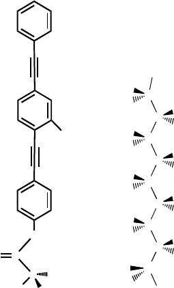
Figure 4 Molecules used for self assembling. 1 yields the 4 4
-(diethynylphenyl)-2
-nitro-1-
benzenethiolate during self-assembly wherein the acetyl group (COCH
3
) is cleaved and the sulfur
attaches to the gold islands. 2 is the octyltrichlorosilane. During the self-assembly process, the
three chlorine atoms are displaced by surface hydroxyls on the SiO
2
substrate [50]
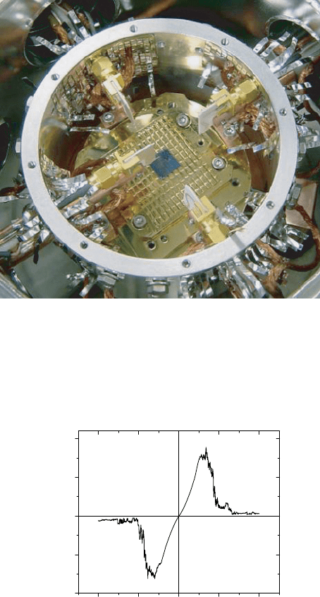
normal operation of the system. In order to exclude this environmental influence, the
sample is placed inside a high vacuum (about 10
−7
torr) chamber (Figure 5) during the
measurement.
The temperature of the sample stage inside the vacuum chamber can be reduced by
a continuous flow of liquid nitrogen, which is pumped out from a nitrogen dewar by a
flow of nitrogen gas. A temperature sensor is attached to the sample holder inside the
vacuum chamber. The other end of the temperature sensor is connected to a temperature
controller. Users could input the set point of the desired temperature and the temperature
controller calculated the output power of a heater, which is located at the chamber wall,
based on the difference between the desired and the current temperature. Thus, the
temperature gradually approaches the set point. In this chapter, the nanoCell devices are
analyzed at room temperature (297 K).
The electrical measurement is performed by a HP 4145 semiconductor parameter
analyzer remotely controlled by a computer. The applied voltage is swept in a staircase
manner from start voltage V
1
to stop voltage V
2
in a voltage step of V . The current is
measured at the end of each voltage step.
2.4. Electrical characteristics of nanoCells
Current–voltage measurement is carried out on the simple structure with only two
opposing electrodes. There are only OPE molecules self-assembled in the nanoCell.
Analysis of programmable molecular electronic systems 105
Figure 5 Probe station (Lakeshore Cryogenic) used to measure the nanoCell device. The probe
station provides a high vacuum environment (∼10
−7
torr) to eliminate any free particles in the
neighborhood of the sample
–10 –5 0 5 10
–1.0
–0.5
0.0
0.5
1.0
I (mA)
V (V)
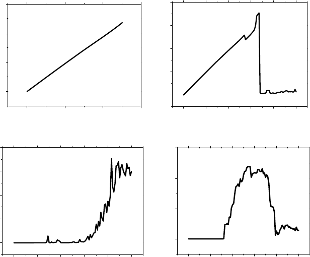
Figure 6 Typical NDR-like behavior shown in nanoCell device
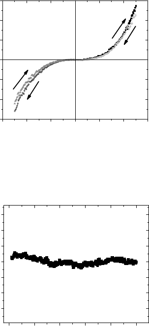
Most of the devices tested exhibit NDR-like behavior, as shown in Figure 6, i.e., the
current changes inversely according to the applied voltage. Thus, NDR-like behavior
has two conductive states at the same current. The current peak value and position,
and even the number of peaks may vary for each device. In addition, the devices show
similar current–voltage characteristics under both polarities of biased voltage, although
the peak value and the position may not be exactly the same.
106 Yuefei Ma and Jorge M. Seminario
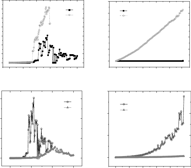
2.4.1. Transition states before NDR
Initially, no NDR behavior is found in the nanoCells; instead, transition states are
found before NDR appeared. Based on the tested nanoCells, 50% of them exhibit
initial transitional behavior as shown in Figure 7. During the first voltage sweeps from
0 to 5 V, the nanoCell exhibits repeatable linear I-Vs (Figure 7a). When the voltage
sweeps from 0 to 10 V, the current drops sharply at a certain voltage V
th1
=∼68V
(Figure 7b). When a voltage less than 6 V is applied, the current is relatively low,
between 9 and 10 nA, as shown in Figure 7c. If the voltage is above 6 V, the current
increases about 3 orders of the magnitude, as shown in Figure 7c. Therefore, voltage of
6 V is defined as the threshold voltage, which is denoted as V
th2
. Repeatable NDR-like
characteristics appear in the subsequent voltage sweeps (Figure 7d). This sequence of
events is referred to as the first observed initial transitional behavior, which is composed
of a high conductance ohmic behavior (Figure 7a), a breakdown behavior (Figure 7b)
and a transitional behavior (Figure 7c).
The initial transition states of the other 50% of the nanoCells do not contain the high
conductance ohmic behavior and the breakdown behavior. Instead, they contain only the
transitional I-V. It is referred to as the second observed initial transitional behavior. For
6
0.0
(a)
(c)
(b)
(d)
0.2
0.4
0.6
I (mA)
V (V)
10
0.0
0.2
0.4
0.6
0.8
I (mA)
V (V)
10
0
2
4
6
8
I (μA)
V (V)
10
0.0
0.2
0.4
0.6
I (mA)
V (V)
024
02468
02468
2
0
4
6
8
Figure 7 First observed current–voltage transition behavior of a nanoCell device. (a) high
conductance ohmic I-V from 0 to 5 V; (b) breakdown once the bias voltage exceeds ∼68V;
(c) transitional I-V, low current increases sharply at about 6 V; (d) NDR-like behavior [50]
Analysis of programmable molecular electronic systems 107
the last 10% of the nanoCells, the transitional I-V does not occur before NDR appears.
It is referred to as the third observed initial transitional behavior.
An interesting feature of all these three transitional behaviors is that it is not reversible,
i.e., the nanoCell cannot be switched back to the original state by the application of
a biased voltage. For instance, for the first observed one, once the NDR appears, the
ultra-high conductance ohmic behavior cannot be observed. In addition, on unbiased
nanoCell devices, negative voltage sweeps also induce similar sequences of I-Vs and
finally reach the NDR-like behavior. However, on biased nanoCells, after the NDR has
appeared in the forward biased range, it also shows up in the negative biased range
without the initial and transitional sequence of I-Vs, and vice versa.
2.4.2. Memory phenomenon in nanoCells
Memory is another phenomenon that has been observed in a nanoCell. Based on the
forward biased I-V characteristics which indicate NDR characteristics, as shown in
Figure 7d, the operating voltage range of the nanoCell can be obviously divided into two
regions separated by a threshold voltage V
T
. When the applied voltage is confined below
V
T
, the I-V curve is relatively smooth and follows a predictable track. When the voltage
goes beyond V
T
, the I-V curve becomes less predictable and includes one or several
negative resistance regions. The interesting feature of nanoCell is that the conductance
of the first region can be changed by applying a voltage beyond the second region.
As shown in Figure 8, if a voltage sweep with stop value higher than V
T
is applied
(curve 1 in Figure 8a), the next voltage sweep with stop value lower than V
T
yields a
low conductance of around 55×10
−8
−1
(curve 1 in Figure 8b). This low conductance
can be switched to high conductance by applying another voltage sweep with stop
value higher than V
T
(curve 2 in Figure 8a). The resulting conductance is around
17 ×10
−5
−1
(curve 2 in Figure 8b). Thus, the process of applying a voltage that is
higher than V
T
is “write”, while the process of applying a voltage that is lower than V
T
is “read”. If we assign the high conducive state “1” or “on” and low “0” or “off ”, the
nanoCell can be switched between “1” and “0” by applying the writing process.
The assignment of “1” and “0” to different conductive states is arbitrary since the
conductance of the read I-V is dependent on the final current value of the writing
process. For example, the conductance curves 1 and 2 in Figure 8d are both low if we
compare them to curve 1 in Figure 8b. However, it is obvious that they are different
since their corresponding conductance are 55×10
−8
−1
and 10×10
−9
−1
for curves
1 and 2, respectively. Certainly, in order to insure a high on–off ratio, these conductive
states will not be used to differentiate “1” and “0”.
Both conductive states are repeatable, i.e., any subsequent read voltage sweep gen-
erates similar I-V curve as in the previous one. Besides, switching between the two
conductive states is repeatable, i.e., any induced conductive state can be switched to
the other one by applying a write voltage. In addition, as shown in Figure 9, the read
voltage is reversible, i.e., the I-V characteristics generated from reverse read voltage
sweep also follows the same pattern.
Switching could also be carried out by applying a voltage pulse. Similarly, reading
can be done by a constant voltage. For example, for the nanoCell that already shows
a “0” state, if a voltage pulse of 6 V for 0.05 second is applied, a higher current is
obtained at a read voltage of 2 V (Figure 10).
108 Yuefei Ma and Jorge M. Seminario
10
0
50
100
150
200
250
300
350
(a)
(c) (d)
(b)
1
2
I (μA)
V (V)
20
46
8
I (μA)
V (V)
2.5
0.00
0.05
0.10
0.15
1
2
0.0 0.5 1.0 1.5 2.0
I (μA)
V (V)
15
0
50
100
150
1
2
0510
I (μA)
2.5
0
10
20
30
40
50
1
2
V (V)
0.0 0.5 1.0 1.5 2.0
Figure 8 Repeatable memory effect in a nanoCell with V
T
=3V. (a) Writing process in which
the final currents are 38 and 219 A for curves 1 and 2, respectively; (b) reading process in
which the conductance are 55 ×10
−8
−1
and 17 ×10
−5
−1
for curves 1 and 2, respectively;
(c) writing process in which the final currents are 38 and 8 A for curves 1 and 2, respectively;
(d) reading process in which the conductance are 55 ×10
−8
−1
and 10 ×10
−9
−1
for curve
1 and 2, respectively
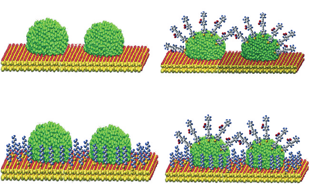
One interesting experiment is to prepare and test four different ensembles (Figure 11)
by depositing different combinations of molecules 1 and 2. The first ensemble has only
the discontinuous gold film; the second one has molecule 1 self-assembled on the gold
islands of the discontinuous gold film; the third ensemble has molecule 2 self-assembled
on the silicon oxide of the substrate; and the fourth one has 1 and 2 self-assembled on
the gold islands and SiO
2
, respectively.
2.5. Influence of molecules on electrical behavior
It is expected that the first and the third ensemble should have extremely low conduc-
tance, since alkane and vacuum are both good insulators; the fourth ensemble should
have a conductance somewhat in-between. However, the four ensembles showed similar
Analysis of programmable molecular electronic systems 109
3
–3
–2
–1
0
1
2
3
I (nA)
V (V)
–3 –2 –1 0 1 2
Figure 9 Read conductance in forward and reverse biases. The arrows indicate the direction of
applied voltage
5
22
23
24
25
26
27
28
I (μA)
t (s)
012
34
Figure 10 A read current at 2 V vs time after a write voltage of 6 V for 0.05 second
I-V characteristics with peak current values in the same order of magnitude. Thus, we
reach the conclusion that the above observed behavior is due to the electron migration
through discontinuous gold film.
In order to further investigate the influence of molecules on the nanoCells’ electrical
behavior, one of the chips with nanoCells featuring NDR is cut into two pieces. Molecule
OPE is deposited on one-half of the chip and alkane molecule on the other half of
the chip.
The nanoCells with OPE molecule (Figure 11b) exhibit similar switching character-
istics like the nanoCells with only the discontinuous gold film (Figure 3a), including a
similar threshold voltage and NDR peak value. This further demonstrates that only the
formed gold filaments are responsible for the NDR behavior or at least that the contribu-
tion of the OPE to the electron conductance is negligible compared to the contribution
of the filaments.
110 Yuefei Ma and Jorge M. Seminario
(a)
(c)
(b)
(d)
Figure 11 Schematic drawings of four ensembles of the nanoCells with (a) only the discon-
tinuous gold film on SiO
2
; (b) molecule 1 deposited on the discontinuous gold film islands;
(c) molecule 2 deposited on the silicon oxide surface; (d) molecules 1 and 2 deposited on gold
and SiO
2
, respectively
The nanoCells with alkane molecule (Figure 11c) self-assembled on SiO
2
show
increases in threshold voltage V
th2
(∼10 V higher). This means that the insulating alkane
molecule creates a higher barrier for the electron transfer through gold islands. After
reaching V
th2
, the barrier is overcome and we obtain an NDR characteristic similar to
those found without any molecule or with only OPE. We carry out deposition of alkane
on the chips already containing molecule OPE (Figure 11d). This fourth ensemble
(Figure 3d) exhibits behavior similar to the third ensemble (Figure 11c), which is
consistent with our previous conclusion that the I-Vs of the nanoCell with and without
OPE are very similar.
To further investigate the influence of the OPE, we deposit the OPE on a chip where
no current is found. After deposition, there is still no current. This, again, proves that
the OPE has no significant influence on the I-Vs of the nanoCells.
2.6. Programming of nanoCell
The nature of randomness on addressing molecules inside the nanoCell makes this
device dependent on computer programming.
In a multi-leads nanoCell, each pair of the leads shows similar switching and memory
phenomenon as in the two-lead nanoCell. Once a conductive state has been written
to one of the lead pairs, the conductance of the same nanoCell between the other
pairs changes accordingly. During the measurement, only the two leads of interests are
connected to the semiconductor parameter analyzer, while others are dangling. Take the
nanoCell shown in Figure 12 as an example. When the conductive state between K and
Analysis of programmable molecular electronic systems 111
A
E
BC
KOM
J
I
H
G
F
P
Q
R
S
T
NL
D
Figure 12 Multiple-leads nanoCell with alphabetic notation on each lead
ABCDEFGHI J KLMNOP QRS T
A
X1111000001111111111
B
1X111000001111111111
C
11X11000001111111111
D
111X1000001111111111
E
1111X000001111111111
F
00000X00000000000000
G
000000X0000000000000
H
0000000X000000000000
I
00000000X00000000000
J
000000000X0000000000
K
1111100000Xa00000000
L
11111000000X
a
0000000
M
111110000000X
a
111111
N
1111100000000X
a
00000
O
00000000000000X00000
P
111110000000000X
a
000
Q
1111100000000000X
a
00
R
00000000000000000X
aa
S
000000000000000000X0
T
1111100000000000000X
D
S
Figure 13 Truth table of a nanoCell as K–E is set to “1”. The truth value in any entry is
measured between the drain-terminal (D) and the source-terminal (S) when a voltage sweep is
applied to the drain
E is set to “1”, the conductive states between other pairs of leads are summarized in
Figure 13.
Three kinds of conductive states exhibit on this nanoCell. The “1” and “0”
correspond to the high (higher than 10
−6
−1
) and low conductance (lower than
10
−6
−1
), respectively. These are expected to be observed. However, there is a third
state with high conductance and ohmic behavior which is similar to the initial transi-
tional behavior in the two-leads nanoCell. In the programming of nanoCell, this kind of
conductance can be ignored.
The programming of nanoCell can be carried out using a multiple probe testing
board and computer controlled oscilloscope. The fundamental idea is to first collect all
the switching information between each leads. For example, the switching information
between KE when KE is “1” has been obtained. The switching information between
112 Yuefei Ma and Jorge M. Seminario
KE when KE is “0” also needs to be obtained. Similarly, the information between AB,
CD, JO, etc. needs to be obtained. Once a database of switching information is formed,
the computer calculates the specific pair of leads that a voltage pulse can write into to
perform desired function.
3. Electrical conductance of discontinuous metallic film
In this section, first the theoretical models proposed by several researchers to explain
the electrical conductance through discontinuous metallic films are outlined. Then the
electrical conductance is investigated both experimentally and theoretically in two
categories: below the threshold voltage and beyond the threshold voltage.
3.1. Theoretical models in discontinuous metallic film
Since nanoCells with only discontinuous gold film have large current (>1A) and
exhibit memory and switching phenomena, the understanding of the electrical conduc-
tance of discontinuous metallic film becomes critical for the analysis of programmable
molecular array. It will not only benefit the research work in discontinuous-metal-film-
based nanoCell, but also provide in-depth knowledge of electron transport through any
two-dimensional molecular array. Since the molecules that will be used in the pro-
grammable molecular array are semiconducting, ultimately the programmable molecular
array can be viewed as a two-dimensional array of electron transport junctions, as the
discontinuous metallic film does.
As early as 1960s, electrical conductance through discontinuous thin metal films
has been studied by a number of researchers. Non-ohmic behavior of the electrical
conductance have been observed in several types of discontinuous metal film [53–56].
Neugebauer et al. proposed that when island sizes and separations between them are
both small, activated tunneling of electrons is the dominant mechanism of electron
transfer [57]. The barrier to tunneling is the energy difference between a Fermi-level of a
particle and the lower edge of the conduction band of the substrate. Hill et al. developed
a two-island model to account for the transport. However, Uozumi et al. argued that
the non-ohmic conductance arises from non-ohmicity of the tunneling current at high
electric field, and the expression for the current density is given in [58]. They also
found that the non-ohmicity occurs when the electric field between the two metal islands
exceeds the critical field E
c
, which is defined in [58]:
E
c
=kT/ed (1)
where k is the Boltzman constant, T is the temperature, e is the electron charge, and d
is the island separation.
Uozumi et al. extended the two-island model to one-dimensional series-connected
islands with identical sizes but different gap lengths [59]. Their computational result
showed that the voltage between two islands can be about a hundred times higher than
the average voltage calculated from the one between the two electrodes and that the
logarithm of the conductance depends almost linearly on the square root of the voltage
Analysis of programmable molecular electronic systems 113
between the two electrodes above the threshold voltage [59]. Their experimental results
further confirmed their suggestion [60].
A tremendous breakthrough was accomplished by Shin et al., who proposed a ring-
shaped model to account for the transport properties [61, 62]. In this model, the ring-
shaped array of small islands is located between the two electrodes. Thus, unlike the
one-dimensional arrays proposed by others [58–60, 63–68], there are two branches or
paths for electron transfer. Electrons may get trapped in one of the islands [69]. Thus,
multiple Coulomb blockade gaps may appear in current–voltage characteristics [61] as
current peaks followed by NDR behavior. This is the distinct feature of this model
in contrast to the linear one-dimensional array. In addition, trapped electrons block
the electrical conduction through the array, so no current flows. Using Monte Carlo
simulation, Shin et al. were able to calculate the current for constant voltage between
the two electrodes.
Interestingly, NDR and memory phenomena have been observed and reported in thin
insulating films made of SiO [70] and in organic light emitting diodes [71–82]. Tang
et al. found that for those devices, nanosized metallic islands exist inside the insulating
film. Thus, they explained the NDR and memory phenomena based on the ring-shaped
model of four islands [83]. The state that the trapped electrons block the conductance
path is the “off ” state; otherwise it is “high”. The thermal fluctuations results in the
transition between “on” and “off ”, thus the NDR appears [83]. When the temperature
increases, the current peak broadens. In addition, The memory effect is due to the
“charging” and “discharging” of the electrons in the system [83].
3.2. Electron transport through discontinuous metallic film
below activation energy
As it is mentioned in the last chapter, the current–voltage characteristics of nanoCell can
be divided into two regions: below V
T
, the current increases with increasing voltage and
the I-V curve follows a predicted behavior; beyond V
T
, the I-V curve changes violently
and include one or several local current maximum.
When the applied voltage is below V
T
, the I-V characteristic is relatively smooth for
both low conductance and high conductance. In order to find out the electron conduction
mechanism, we performed a temperature variant current–voltage measurement on the
nanoCell sample that carries room temperature I-V curves shown in Figure 14. There
are no molecules deposited on the discontinuous film. Thus, the gaps between the gold
islands are considered as vacuum.
Interestingly, although discontinuous gold film is a two-dimensional array of junc-
tions, the electrical characteristics resembles the one that is predicted by Uozumi et al.
Figure 15 shows the electric field dependence of the high conductance G of a discon-
tinuous gold film at various temperatures. The electric field is calculated directly from
the applied voltage by dividing by 2 ×10
−4
cm, which is the distance between the two
electrodes for this particular sample. The interesting feature of these curves is that a
remarkable ohmic conductance can be observed beyond 220 K at low electric fields,
i.e., around 20 (V/cm)
−1/2
.
Thus the critical applied field strength from 220 K to room temperature is 400 V/cm.
A second interesting point is for all temperatures, there is another critical applied field