Ramanathan Sh. (Ed.) Thin Film Metal-Oxides: Fundamentals and Applications in Electronics and Energy
Подождите немного. Документ загружается.

262 G.D. Stucky and M.H. Bartl
The first category is of great historical importance, since the original discovery of
mesostructured materials and their structural characterization were based on silica
compounds [14, 15]. Furthermore, mechanistic studies on silica mesostructured
composites contributed greatly to the understanding and control of the chemistry
and physics behind mesostructure formation [23, 24]. However, the insulating na-
ture of silica mesostructures limits their direct use to rather passive application in
sorption, catalysis, and separation in which the mesostructured architecture merely
acts as a high-surface area, high-porosity framework [28,29], or as low-k dielectric
materials for electronic chip applications by making use of their large pore volume
fractions [45].
An important step toward functional composites was the discovery that
mesostructured silica materials are an excellent host for optically active species
such as dyes and organometallic complexes. It was shown that the defined nanoscale
separation in these composites can be used to incorporate guest species into different
nanodomains and thereby greatly enhance their dispersion, even at high loadings
[6, 46]. As a result, the incorporated active species displayed high photolumines-
cence quantum yields, leading to applications of these functionalized composites
as low-threshold mirrorless lasers, fast-responsive optical sensors and switches, and
energy up-conversion systems (for recent reviews on these materials see references
[5, 6, 47, 48] and references cited therein). However, it should be noted that even
in these functionalized silica composites the mesostructure itself acts as a passive
host framework for the functional guests. The true transition from passive to active
mesostructured frameworks took place with the development of transition metal
oxide mesostructured materials (see Table 8.1)[16, 17, 26–28]. The ability to fab-
ricate these materials with nanocrystalline semiconducting framework makes them
inherently functional mesostructures and thereby largely expands the field of poten-
tial applications. Especially, the discovery to process these transition metal oxide
mesostructured materials as nanocrystalline thin films [17] opens new avenues
for advanced optical, electrical, and optoelectronic applications in solar energy
conversion, photocatalysis, and as photoluminescent and electrochromic materials.
Periodically organized nanocrystalline mesostructured thin films possess sev-
eral desirable materials characteristics and therefore are unique members of the
large family of optoelectronically active materials. While the three-dimensional
mesostructural order provides a fully accessible, continuously porous structure
with a pre-defined nanodomain organization and high surface/interface area, the
semiconducting transition metal oxide framework introduces electronic and op-
toelectronic functionalities. Moreover, due to the nanocrystalline nature of the
framework, the electronic and optoelectronic properties can be tuned by controlling
the size of the nanocrystals and/or incorporating dopants into the nanocrystalline
framework. The combination of these different functionalities and structural char-
acteristics within a single material, however, also imposes a great challenge with
respect to synthesis, processing, and integration of such mesostructured composites.
In the following section, we will discuss the main synthesis and processing pa-
rameters of periodically organized mesostructured transition metal oxide thin films
and how these parameters influence structural properties and function. The objective

8 Mesostructured Thin Film Oxides 263
Table 8.1 Physicochemical properties of some periodically organized mesostructured metal oxides. Adapted with permission from Macmillan Publishers Ltd:
reference [17], copyright (1998)
Oxide
Inorganic
precursor
d
100
(
˚
A)
Wall
structure
Wall
thickness
(
˚
A)
Nanocrystal
size
(
˚
A)
Pore size
(
˚
A)
BET surface area Physical
properties
.m
2
g
1
/.m
2
cm
3
/ Porosity
ZrO
2
ZrCl
4
106 Tetra. ZrO
2
65 15 58 150 884 0:43 Dielectric
TiO
2
TiCl
4
101 Anatase 51 24 65 205 867 0:46 Semiconductor
Nb
2
O
5
NbCl
5
80 Nb
2
O
jj
5
40 < 10 50 196 876 0:50 Dielectric
Ta
2
O
5
TaCl
5
70 Ta
2
O
jj
5
40 < 10 35 165 1;353 0:50 Dielectric
WO
3
WCl
6
95 WO
3
50 20 50 125 895 0:48 Semiconductor
SnO
2
SnCl
4
106 Cassiterite 50 30 68 180 1;251 0:52 Semiconductor
E
g
D 4:05 eV
HfO
2
HfCl
4
105 Amorphous 50 – 70 105 1;016 0:52 Dielectric
A1
2
O
3
AlCl
3
186 Amorphous 35 – 140 300 1;188 0:61 Dielectric
SiO
2
SiCl
4
198 Amorphous 86 – 120 810 1;782 0:63 Dielectric
Si
2
AlO
3:5
SiCl
4
=AlCl
3
95 Amorphous 38 – 60 310 986 0:59 Dielectric
Si
2
AlO
5:5
SiCl
4
=AlCl
3
124 Amorphous 40 – 100 330 965 0:55 Dielectric
SiTiO
4
SiCl
4
=TiCl
4
95 Amorphous 50 – 50 495 1;638 0:63 Dielectric
Al
2
TiO
5
AlCl
3
=TiCl
4
106 Amorphous 40 – 80 270 1;093 0:59 Dielectric
ZrTiO
4
Zrcl
4
=TiCl
4
103 Amorphous 35 – 80 130 670 0:46 Dielectric
ZrW
2
O
8
ZrCl
4
=TiCl
4
100 Amorphous 45 – 50 170 1;144 0:51 NTE
#
All samples were prepared using ethanol as a solvent except HfO
2
where butanol was used. The structure-directing agent in all cases was EO
20
PO
70
EO
20
(see
text). The aging process generally took 1–7 days.
d-values of 100) reflection for samples calcined at 400
ı
Cfor5hinair.
Thicknesses measured from TEM experiments. These values are consistent with the values estimated by subtracting the pore diameter from 2d
100
=
p
3.
Nanocrystal sizes estimated from X-ray diffraction broadening using the Scherrer formula.
The porosity is estimated from the pore volume determined using the adsorption branch of the N2 isotherm curve at the P=P
0
D 0:983 single point.
jj
Nucleation just started, extremely broad wide-angle diffraction.
‘
Direct allowed optical gap estimated from .˛hv/
2
hv plot of UV-vis absorption measurement where a lathe absorption coefficient.
#
Materials with negative thermal expansion properties.
264 G.D. Stucky and M.H. Bartl
is to provide general insights into the critical parameters of mesostructure formation
and framework nanocrystallization rather than to give a detailed discussion about
specific synthesis conditions and processing parameters. We will use mesostruc-
tured nanocrystalline titania .TiO
2
/ films as an example due to its great importance
in optoelectronic and photocatalytic applications [3, 8,49–51].
8.3.2 Assembly and Nanocrystallization of Titania Mesoporous
Thin Films
Among transition metal oxide photocatalysts, the wide band gap semiconductor
titanium dioxide (titania, TiO
2
) occupies a special position due to its outstand-
ing chemical and physical properties, possessing a high catalytic activity, chemical
stability, and non-toxic properties [52]. Moreover, it was found that these properties
are enhanced when titania is fabricated in nanocrystalline form, mostly due to the
quantum size effect and increased charge separation and transfer processes [52,53].
The central aim of mesostructure synthesis is to combine these desired properties
of titania nanocrystals with the characteristics of mesostructured materials (such as
periodically organized porosity, high surface/interface area and three-dimensionally
accessible nanostructure) and thereby further enhance the photocatalytic activity.
In general, the fabrication process of mesostructured thin films can be divided
into two main steps: sol–gel cooperative assembly and framework nanocrystal-
lization. Mesostructure formation through a cooperative assembly process occurs
upon solvent evaporation during thin film processing. As discussed in Sect. 8.2.2,
this is accomplished by either dip or spin-coating the precursor solution contain-
ing both the hydrolyzed molecular titania entities and the mesostructure-directing
organic species (e.g., non-ionic block copolymers). A key consideration for success-
ful mesostructure formation is to first convert the highly reactive titania precursors
(such as titanium tetrachloride or alkoxides) into stable and soluble hybrid interme-
diate entities. The purpose is to slow condensation kinetics of the titania precursor
entities, in order to give structure-directing surfactant species enough time to or-
ganize the inorganic components. Successfully applied techniques to slow titania
condensation include the use of ligand-assisted templating, metal chloride solvolysis
in alcohols, acid/base reactions of metal salts and alkoxides in alcohol solvents, and
pre-hydrolysis routes of metal alkoxides in strongly acidic aqueous environments
[16, 17, 27, 54–61]. Additionally, a recent approach that has proven to be particu-
larly successful is the in situ formation of uniformly sized nanoparticles, generally
3–10 nm in diameter (depending on reaction conditions and composition) using ac-
etate coordination [62]. In all cases, the stabilized inorganic titania entities are then
assembled and organized by the structure-directing organic species into a given ther-
modynamically stable mesostructure phase, which is determined primarily by the
volume ratio of inorganic species to surfactant, the temperature, and the humidity
during and after the film formation process [42,44,54].
Assembly is followed by a controlled heat treatment of the films during which
they transform from a periodically organized liquid–crystalline mesostructured
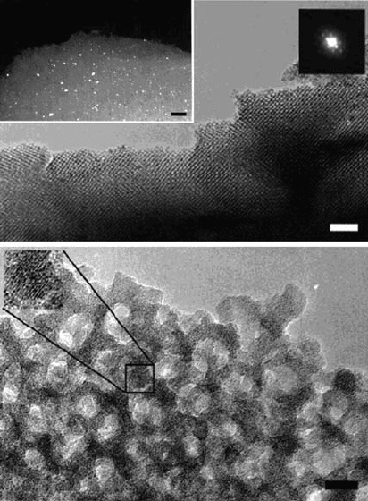
8 Mesostructured Thin Film Oxides 265
composite with solubilized molecular titania species or nanoparticles into a meso-
porous framework built of anatase nanocrystals and amorphous titania. For this,
the films are first kept in an oxidative high-temperature environment to remove the
organic surfactant phase and simultaneously promote condensation/solidification
of the titania entities. The condensation is then followed by nucleation and growth
of semiconducting anatase nanocrystals out of the amorphous titania matrix as
depicted in Fig. 8.5.
Both the relative amounts of the nanocrystalline and amorphous phases and the
size of the anatase nanocrystals can be varied within a certain range simply by
fine-tuning the heat treatment and nanoparticle building block synthesis described
previously. While the maximum size of the nanocrystals is naturally limited by
the thickness of the mesopore walls, the relative nanocrystal concentration is lim-
ited by structural stability issues. In particular, a certain amount of amorphous
Fig. 8.5 Transmission electron micrographs of a periodically cubic ordered mesostructured titania
thin films. Top: Plan-view image of the cubic mesostructural order. Scale bar: 100 nm. Inset right:
Small-angle electron diffraction pattern from a selected area. Inset left: Dark-field transmission
electron micrograph of the cubic film sample, where individual nanocrystallites diffract into an
off-center objective aperture and thus appear bright. Scale bar: 100 nm. Bottom: A high-resolution
micrograph of the cubic mesostructured thin film, showing nanocrystallites in random orientations
with lattice fringes corresponding to the crystalline anatase structure. Scale bar: 10 nm. Adapted
with permission from reference [54]. Copyright (2002) American Chemical Society
266 G.D. Stucky and M.H. Bartl
titania is needed to effectively sustain the local strain caused by crystallization
and prevent the mesostructure from collapsing. As we will discuss in the follow-
ing section, the co-existence of nanocrystalline and amorphous titania phases is
vital for the incorporation of dopant ions and for the fabrication of titania-based
multi-compositional oxide or mixed-oxide-chalcogenide mesostructured materials.
However, for direct applications in solar energy conversion and photocatalysis, an
only-partially nanocrystalline framework is a disadvantage and reduces the photon-
to-energy conversion efficiency, since the catalytic activity and the framework
conductivity (electron hopping mechanism), and electron-hole recombination, are
directly related to the degree of crystallization. Tang et al. showed that the de-
gree of framework crystallinity can be significantly increased, if the mesoporous
framework is first completely infiltrated with a structure-stabilizing material such
as amorphous carbon [51]. In this case, the high curvature of the porous structure
is sufficiently supported, allowing the complete crystallization of the mesoporous
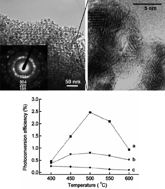
framework under prolonged heat treatment. Such highly crystalline mesoporous
structures display drastically enhanced conversion efficiencies as shown in Fig. 8.6.
For example, periodically ordered mesoporous titania thin films heat-treated at
500
ı
C for an extended time yielded a water photolysis (“water-splitting”) pho-
toconversion efficiency of 2.5% at zero-bias conditions and under illumination at
40 mW=cm
2
by a xenon lamp [51].
8.4 Multi-Compositional Mesostructured Thin Film Oxides
The flexibility of sol–gel cooperative assembly chemistry makes it possible
to extend the simple single-precursor approach to the fabrication of multi-
compositional mesostructured materials. As we will discuss in this section, the
three-dimensional arrangement and integration of different functional units within
the nanocrystalline mesostructure framework enables their constructive interaction
and results in materials systems with cooperative functionalities. Examples of
such functional units are rare-earth ion and nitrogen dopants, lithium ions, mixed
transition metal oxide arrays, and metal chalcogenide nanocrystals.
8.4.1 Optical, Electrical, and Electrochemical Applications
Frindell et al. demonstrated that trivalent rare earth ions – a technologically im-
portant class of narrow bandwidth emitters – can be doped into the two-phase
nanocrystalline/amorphous framework of mesoporous titania thin films simply by
incorporating rare earth ion chlorides into the titania/surfactant precursor solution
[62–65]. From a fabrication standpoint, rather surprisingly, it was found that rare
earth ion doping, if anything, improved the quality of the mesostructure long-
range order. More importantly, however, the authors showed that these composite
8 Mesostructured Thin Film Oxides 267
Fig. 8.6 Highly crystalline periodically ordered mesoporous titania thin film samples fabricated by
a carbon-assisted high-temperature .550
ı
C/ crystallization technique. Top: Transmission electron
micrographs showing mesostructural ordering (left) and highly crystalline framework wall compo-
sition (right). Bottom: Photoconversion efficiencies for different titania samples under 40 mW=cm
2
illumination and at zero-bias. a: Ordered mesoporous titania with highly crystalline wall struc-
ture. b: Disordered/collapsed mesoporous titania with highly crystalline wall structure. c: Ordered
mesoporous titania with amorphous wall structure. Adapted from reference [51]. Reproduced with
permission of the Royal Society of Chemistry
mesostructured thin films display efficient cooperative activity. While the amor-
phous titania regions provide an ideal glass-like environment for the incorporation
of rare earth ions, the light-harvesting nature of the anatase nanocrystals can sensi-
tize rare earth ion luminescence through indirect excitation pathways.
Using photoluminescence emission and excitation spectroscopy as well as
anatase titania conduction band and surface state energy analysis, Frindell et al.
studied the sensitization/energy transfer process and showed that the sensitized rare
earth ion emission process is the result of band edge absorption of UV photons
268 G.D. Stucky and M.H. Bartl
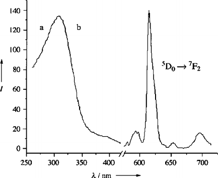
Fig. 8.7 Photoluminescence excitation (a) and emission (b) spectra of cubic ordered
nanocrystalline titania mesostructured films doped with 8 mol% trivalent europium ions. The eu-
ropium crystal field emission lines (right spectrum) were obtained by excitation of the anatase
titania excitonic absorption transition at 330 nm (left spectrum). Taken from reference [63]. Copy-
right Wiley-VCH Verlag GmbH & Co. KGaA
by the wide band gap semiconducting anatase nanocrystals [64]. The absorbed
excitonic energy subsequently relaxes into nanocrystal surface states followed by
non-radiative energy transfer to crystal field states of the rare earth ions located
at the surface of these nanocrystals. This energy is then released through radia-
tive transitions within the rare earth ion crystal field split energy levels, resulting
in efficient narrow bandwidth emission. While initial studies were performed on
red-emitting trivalent europium doped samples (Fig. 8.7), it was demonstrated that
this energy transfer concept can be extended to a number of different rare earth ions,
expanding the range of sensitized narrow bandwidth emission from the visible to the
near-infrared including the technologically significant region around 1,550 nm [64].
Ordered mesostructured thin films are also promising candidates for advanced
electrochemical applications. Reiman et al. [66] and Sallard et al. [67] demon-
strated that nanocrystalline mesoporous thin films of TiO
2
and WO
3
, respectively,
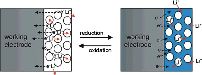
are interesting hosts for the insertion/extraction of lithium (see Fig. 8.8). These
materials exhibit high insertion capacities, fast insertion/extraction kinetics, and
low self-discharge tendencies. In general, both studies concluded that the high
surface/interface area of the mesoporous host framework enables a high density of
electrochemical reaction locations. Furthermore, it was found that for fast kinetics
and large capacities of the lithium insertion highly nanocrystallized frameworks are
of great importance, since the presence of amorphous oxides induces unstable and
short-lived electrochemical performances due to irreversible structural framework
modifications [67].
8 Mesostructured Thin Film Oxides 269
Fig. 8.8 Schematic depicting lithium insertion/extraction into ordered mesoporous thin films.
Adapted with permission from reference [67]. Copyright (2007) American Chemical Society
Another electrically/electrochemically interesting, continuously ordered meso-
structured material was reported by Smarsly and coworkers, who developed
transparent, conducting indium tin oxide mesoporous thin films [68]. For these
composites, which are prepared by doping appropriate amounts of divalent tin ions
into the indium oxide/surfactant precursor solution, it was also found that a high
crystallinity is crucial for good electrical and electrochemical performance. For
example, thin films with no or low crystallinity in their framework exhibited no
measurable conductivity. However, films with a highly crystalline tin-doped indium
oxide framework displayed sheet resistivities of only 3 10
5
, which were further
decreased to values as low as 1:3 10
3
upon heating the samples in a reducing
hydrogen atmosphere. This increase in conductivity (decrease in resistivity) is the
combined effect of a higher crystallinity and an increase in the number of charge
carriers due to the formation of oxygen vacancies. Interestingly, the authors found
that the specific resistivity of these highly porous thin films is only one or two orders
of magnitude higher than that of compact bulk crystalline films, which makes them
promising candidates for use in solar cells as high surface area photoelectrodes [68].
8.4.2 Photocatalytic and Electrochromic Applications
Another interesting doped mesostructured material was reported by Sanchez and
coworkers, who found that nitrogen-doping of a nanocrystalline mesoporous titania
framework can significantly shift the titania absorption band edge [69]. Nitrogen
was doped into the framework by treating the mesoporous samples with ammo-
nia at temperatures ranging from 400
ı
Cto900
ı
C, with the best results obtained
from samples treated at 500
ı
C. The observed shift of the titania absorption band
edge with increasing nitrogen doping is of great importance. Not only does this
method make it possible to continuously modify the band gap energy of this com-
posite material, but it also increases its sensitivity to visible light. In contrast to

270 G.D. Stucky and M.H. Bartl
pure titania mesostructured films, which are transparent to visible photons, nitrogen-
doped samples can be tuned to absorb throughout the visible. This phenomenon is
also exemplified in the strongly enhanced photocatalytic response to visible light
in lauric acid-decomposition. The authors suggest the high activity is due to an
optimal nitrogen concentration in the mesostructure framework such that oxygen
vacancies are not actively involved in the unwanted recombination of the photogen-
erated charge carriers [69].
Besides the incorporation of discrete dopants into the mesostructure frame-
work it is also possible to fabricate mesostructured thin films with walls simul-
taneously composed of different nanocrystalline metal oxide compounds. Starting
from a single cooperative assembly-precursor solution containing solubilized metal
oxide precursors, mesostructured titania composites with incorporated tungsten,
zirconium, cerium, strontium, cadmium and cobalt oxides can be obtained [17,62,
65,70–73].
Interestingly, for all of these composites, an improved mechanical and thermal
stability of the mesostructure framework was reported (see also Table 8.2). More
importantly, however, it was found that composite metal oxide mesostructured thin
films possess both a higher surface area and increased photocatalytic activity. For
example, Frindell et al. found that the incorporation of cerium oxide into a titania
mesoporous framework leads to a large number of interfacial surface states that
act as electron traps [65]. The presence of trapped electrons at interfacial sites
significantly alters the electrochemical properties and results in an increased elec-
trochromic response of titania–ceria mesostructured composites.
Pan and Lee investigated the inclusion of tungsten oxide .WO
3
/ into meso-
porous titania thin films and studied the effect on the photocatalytic properties [73].
A schematic of the formation of mixed TiO
2
=WO
3
mesostructured composites and
a transmission electron image of the resulting mixed nanocrystalline framework is
given in Fig. 8.9 and clearly demonstrates the intimate contact of TiO
2
and WO
3
nanocrystals. The photocatalytic properties of this composite material were deter-
mined by the decomposition of 2-propanol in the gas phase. It was found that a
Table 8.2 Precursor compositions and critical temperatures of crystallization and mesostructure
degradation for different mesostructured mixed metal oxide composites. Adapted by permission
from Macmillan Publishers Ltd: reference [72], copyright (2004)
SrTiO
3
MgTa
2
O
6
CO
0:15
Ti
0:85
O
1:85
KLE3739 0.1259 0.075 g 0.05 g
M1 0.347 g (SrCl2, 6H
2
0) 0.029 g .Mg.OH/
2
/ 0.025 g .CoCl
2
/
M2 0.265 g .TiCl
4
/ 0.42 g .Ta.OEt/
5
/ 0.185 g .TiCl
4
/
EtOH 7.25 g 6 g 3 g
THF 2 g 1 g 1 g
H
2
01.5g – 0.2g
HCl 37% conc – 1.5 g
Crystallization 610
ı
C 760
ı
C 500–570–650
ı
C
Destructuration 660
ı
C 800
ı
C 660
ı
C
Co-doped anatase, ilmenite and co-doped rutile crystallize into the given order.
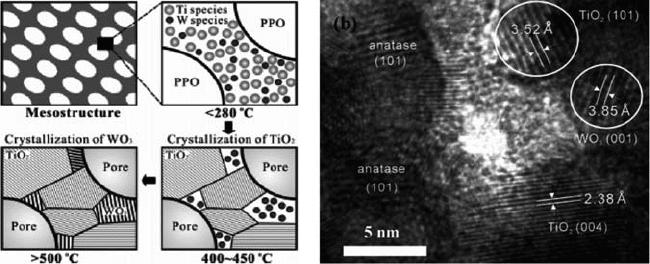
8 Mesostructured Thin Film Oxides 271
Fig. 8.9 Left: Schematic showing the formation of mixed TiO
2
=WO
3
nanocrystalline mesostruc-
tured composites. Right: Transmission electron micrograph displaying the presence of the simul-
taneous presence of TiO
2
and WO
3
nanocrystals in the mesostructure framework. Adapted with
permission from reference [73]. Copyright (2006) American Chemical Society
maximum of photocatalytic activity is reached at a WO
3
concentration of 4 mol%.
At this composition, the activity of cubic ordered mesoporous TiO
2
=WO
3
composite
films was more than twice as high as mesoporous pure TiO
2
thin films and more
than six times higher than nonporous TiO
2
thin films. The authors suggest that the
strongly enhanced photocatalytic activity with an increased surface acidity in the
composite is due to the presence of WO
3
nanocrystals.
Bartl et al. showed that the simple, single-precursor solution strategy that
produces mixed metal oxide nanocrystalline composites can also be applied to
fabricate highly ordered cubic mesoporous frameworks with walls composed of
integrated arrays of different types of wide and narrow band gap semiconductor
nanocrystals, such as anatase titania/cadmium sulfide and anatase titania/cadmium
selenide [3, 70]. The key to the successful fabrication of such mixed nanocrystal
frameworks lies in an extended heat-treatment of dip-coated films under varying
gas/vapor atmospheres. The films are first kept in an oxidative high-temperature
environment to remove surfactant and induce nucleation and growth of semicon-
ducting anatase nanocrystals out of the amorphous titania matrix. Simultaneously,
segregation of the co-assembled cadmium species occurs into cadmium oxide nan-
oclusters evenly distributed in the titania framework. By changing the heat-treatment
atmosphere from oxidative conditions to an inert gas-diluted sulfur or selenium va-
por, the cadmium oxide nanoclusters are selectively converted into semiconducting
CdS or CdSe nanocrystals through a redox-coupled ion exchange reaction mech-
anism. The successful transformation of cadmium oxide into its nanocrystalline
sulfide or selenide analogues is exhibited by a change of the thin film coloration
from transparent to yellow or orange, as shown in Fig. 8.10. The presence of a
mixed nanocrystal wall composition as well as the cubic mesostructural ordering is
also confirmed by transmission electron microscopy imaging in combination with
energy dispersive X-ray spectroscopy and by X-ray diffraction analysis.
