Ramanathan Sh. (Ed.) Thin Film Metal-Oxides: Fundamentals and Applications in Electronics and Energy
Подождите немного. Документ загружается.

190 Y. Hikita and H.Y. Hwang
metal–semiconductor junction can capture any termination dependence of the SBH.
This trend can be understood by considering the evolution of the screening dipole
at the interface, which is expected to be quite general for metal–semiconductor and
metal–insulator perovskite heterointerfaces [88].
Because this interface systematically changes from MnO
2
=La
0:7
Sr
0:3
O=TiO
2
to MnO
2
=SrO=TiO
2
, the sheet charge density shifts from 0:7q=C0:7q=0q to
0:7q=0q=0q, assuming a fully ionic charge assignment using the nominal bulk va-
lence for each grown layer, creating a polar discontinuity at the interface. To avoid
a diverging electrostatic potential arising from the interface, ˙0:35q extra charge
is required at the two interfaces, respectively. Whereas previous considerations of
this effect between two insulators were discussed in terms of electronic reconstruc-
tions [10, 11, 16, 22, 24, 89, 90], here the interface between a metal and a semicon-
ductor is better framed in terms of metallic screening by the La
0:7
Sr
0:3
MnO
3
–the
NbWSrTiO
3
side of the interface being fully depleted.
The estimated Thomas–Fermi screening length of 0:31 nm in La
0:7
Sr
0:3
MnO
3
implies a change in the valence of Mn at the first interface layer in the simplest ionic
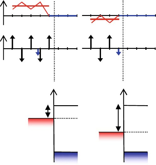
assignment. Thus, as depicted in Fig. 5.18a, the first MnO
2
layer of La
0:7
Sr
0:3
MnO
3
will have extra screening charge. Even after this charge compensation, a finite elec-
trostatic potential remains inside La
0:7
Sr
0:3
MnO
3
relative to NbWSrTiO
3
,givingan
interface dipole which linearly varies with the interface termination. The variation
in the barrier height induced by the difference in the termination at the interface is
estimated using the charge assignment shown in Fig. 5.18. The evolution of the SBH
arising from this ionic dipole is given in Fig. 5.17d, referenced to the Schottky–Mott
relation [79]. The electrostatic potential difference between the two end-member in-
terfaces is 0.54 V. This value, as well as the linearly increasing SBH with varying
interface termination, agrees with the experimentally determined trends. It should be
noted that the ionic limit discussed here is an oversimplification. A more realistic es-
timate of the interface dipole requires incorporation of the hybridization effects and
better understanding of the relevant relative permittivity on very short length scales.
Nevertheless, this basic framework for interface dipole formation should assist in the
design of complex oxide heterostructures and the control of their band alignments.
5.4 Applications of Complex Oxide Schottky Junctions
5.4.1 Magnetoresistance at Manganite/NbWSrTiO
3
Junctions
Perovskites with manganese as the B-site cation show large negative magnetoresis-
tance, termed “colossal magnetoresistance” [91]. Manganites exhibit various ground
states including ferromagnetic metal and charge ordered insulators which can poten-
tially be used to create new functionalities at interfaces. Reviews of the fabrication
techniques and the basic physics of manganites are available in [92].
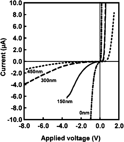
An early attempt to fabricate rectifying heterojunctions using manganites was in
the p–i–n structure using La
0:85
Sr
0:15
MnO
3
=SrTiO
3
=La
0:85
Sr
0:15
TiO
3
on NbWSrTiO
3
5 Complex Oxide Schottky Junctions 191
0.0 uc 1.0 uc
SrMnO
3
coverage
E
E
C
E
F
E
V
E
MnO
2
LSO
MnO
2
MnO
2
LSO
LSO
MnO
2
LSO
LSO
TiO
2
TiO
2
SrO
TiO
2
TiO
2
SrO
SrO
-V
Q
F
SB
F
SB
Fig. 5.18 (a) A schematic diagram of the La
0:7
Sr
0:3
MnO
3
=NbWSrTiO
3
interface charge sheet den-
sity and the electrostatic potential for 0.0 uc (left) and 1.0 uc (right)ofSrMnO
3
coverage. The small
arrows in La
0:7
Sr
0:3
MnO
3
represent the compensation charges induced to screen the interface. The
relative electrostatic potential across the interface varies depending on the interface termination,
consequently changing the band alignment (b) at the interface (From [87], by permission)
[93]. Rectifying I V characteristics were observed which diminished as the i-layer
is decreased (Fig. 5.19).
A demonstration of modulating the magnetism in manganite thin films was
given in .La; Ba/MnO
3
=NbWSrTiO
3
p–n heterojunctions [94]. Here they demon-
strated a continuous modulation of the junction resistance by magnetic field
which they attribute to the modulation of the bulk magnetism of .La; Ba/MnO
3
.
These results triggered the studies of junction magnetoresistance which are
now found in many systems, including La
0:32
Pr
0:35
Ca
0:33
MnO
3
=NbWSrTiO
3
[95, 96], La
0:7
Ce
0:3
MnO
3
=NbWSrTiO
3
[97], La
0:9
Sr
0:1
MnO
3
=NbWSrTiO
3
[98], and
Nd
0:5
Sr
0:5
MnO
3
=NbWSrTiO
3
[99]. The polarity and the temperature dependence
of the junction magnetoresistance are phenomenologically intricate, and further
complicated by the many phase transitions arising from the strong correlation ef-
fects in the manganites. Basic quantities such as band offsets or dopant density
distribution need to be clarified, but have been addressed in only a limited number
of manganite/NbWSrTiO
3
systems [83,87,100,101].
192 Y. Hikita and H.Y. Hwang
Fig. 5.19 I V characteristics of La
0:85
Sr
0:15
MnO
3
=SrTiO
3
=La
0:85
Sr
0:15
TiO
3
p–i–n diodes at
room temperature, where the thickness of the SrTiO
3
layer is varied (From [93], by permission)
In this section, we take an example of a junction exhibiting negative junction
magnetoresistance and examine the temperature dependent I V characteristics in
an attempt to clarify the origin of this intriguing phenomenon. The systems of
interest are La
0:7
Sr
0:3
MnO
3•
=NbWSrTiO
3
junctions [102]. The electrical prop-
erties of La
0:7
Sr
0:3
MnO
3•
and La
0:7
Sr
0:3
MnO
3
thin films grown on insulating
SrTiO
3
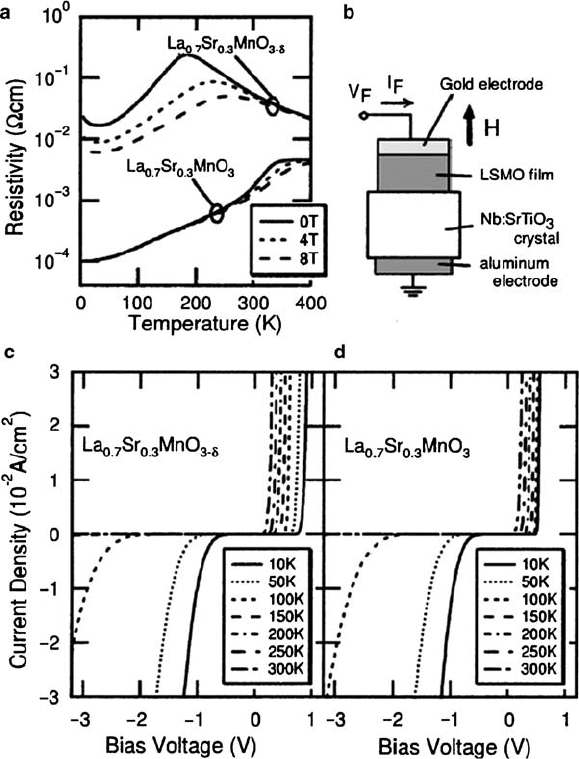
.001/ substrates are shown in Fig. 5.20a. The oxygen deficient film showed
reduced T
C
and increased resistivity accompanied by a larger magnetoresistance.
The temperature dependent IV characteristics of both junctions with the polarity
given in Fig. 5.20bareshowninFig.5.20c, d. The temperature dependence of the
I V characteristics is similar to that of Au=NbWSrTiO
3
[70], with a substantial de-
crease in the breakdown voltage as the temperature is decreased. The forward-biased
I V characteristics show typical exponential dependence on the applied voltage at
high temperatures but below 100K, they deviate from thermionic emission, as will
be discussed later.
Figure 5.21a shows the magnetic field dependence of the La
0:7
Sr
0:3
MnO
3•
junction at 10 K, with the field applied perpendicular to the plane of the junction.
The magnetic field induces a large shift of the forward-bias current to lower volt-
age, with negligible effect on the reverse-bias region after the initial application of
the magnetic field. As can be seen from Fig. 5.21b, a much smaller magnetic field
dependence has been observed for the stoichiometric junction at 10 K.
5 Complex Oxide Schottky Junctions 193
Fig. 5.20 (a) Temperature dependent resistivity for La
0:7
Sr
0:3
MnO
3•
and La
0:7
Sr
0:3
MnO
3
films
in 0, 4, 8 T applied field. (b) Schematic illustration of the junction device and polarity. Tempera-
ture dependence of the I V characteristics of the (c)La
0:7
Sr
0:3
MnO
3•
and (d)La
0:7
Sr
0:3
MnO
3
junctions (From [102], by permission)
To probe the effect of a magnetic field, the low frequency junction capacitance is
measured as a function of magnetic field (Fig. 5.22a) together with the differential
conductance G D dJ=dV at a current density of 20 mA cm
2
under forward-bias
in Fig. 5.22b. The two results indicate that the magnetic field reduces the effective
depletion width, exponentially enhancing the junction magnetoresistance. Due to
the exponential voltage dependence, G increases by almost two orders of magni-
tude in 8 T, while the capacitance increases by 33%. With increasing temperature,
both the junction magnetocapacitance and the magnetoresistance diminish, main-
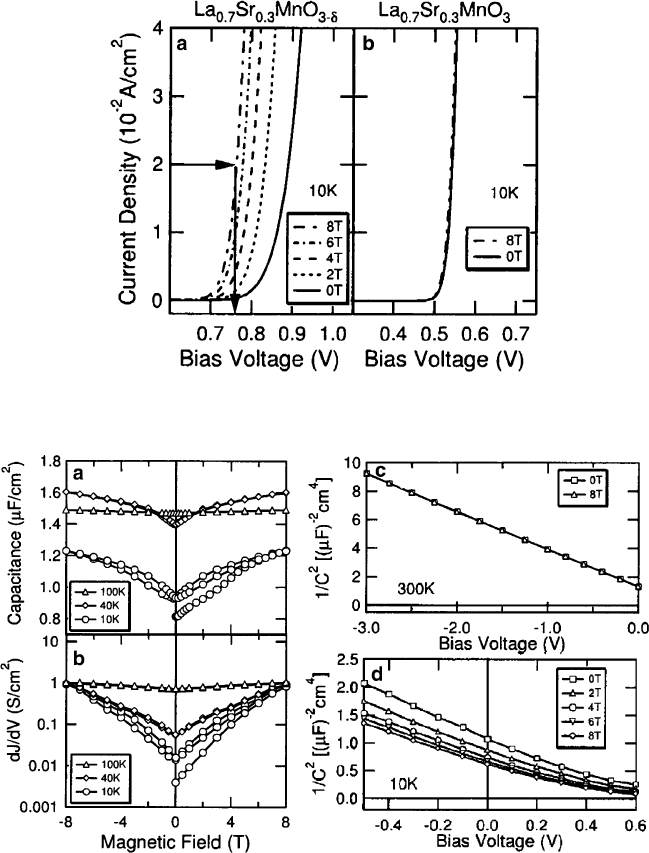
194 Y. Hikita and H.Y. Hwang
Fig. 5.21 Magnetic field dependence of the (a)La
0:7
Sr
0:3
MnO
3•
and (b)La
0:7
Sr
0:3
MnO
3
junctions at 10 K (From [102], by permission)
Fig. 5.22 Magnetic field dependence of the La
0:7
Sr
0:3
MnO
3•
junction characteristics at various
temperatures. (a) Zero-bias capacitance and (b) differential conductance for magnetic field sweeps
across ˙8 T. (c) 1=C
2
as a function of bias voltage at 300 K in 0 and 8 T field. (d) 1=C
2
as a
function of bias voltage at 10 K in varying magnetic field (From [102], by permission)
taining this direct relationship. The stoichiometric junction, by contrast, has little
magnetocapacitance at all temperatures.
The room temperature C V characteristic of La
0:7
Sr
0:3
MnO
3•
junction is lin-
ear and magnetic field independent as can be seen in the 1=C
2
V plot (Fig. 5.22c).
5 Complex Oxide Schottky Junctions 195
However, at low temperatures, 1=C
2
is strongly dependent on the magnetic field
(Fig. 5.22d) which is consistent with the results of Fig. 5.22a, b. The non-linearity
of the curves arises from the electric field dependent relative permittivity of SrTiO
3
discussed earlier.
Further analysis of the I V characteristics of these magnetoresistive junc-
tions revealed that the transport mechanism is again governed by thermionic-field
emission in the cases of La
0:7
Sr
0:3
MnO
3
and La
0:7
Sr
0:3
MnO
3•
junction at 0 T.
However, the transport process of the La
0:7
Sr
0:3
MnO
3•
junction under magnetic
field cannot be explained within the conventional framework of thermionic-field
emission [103].
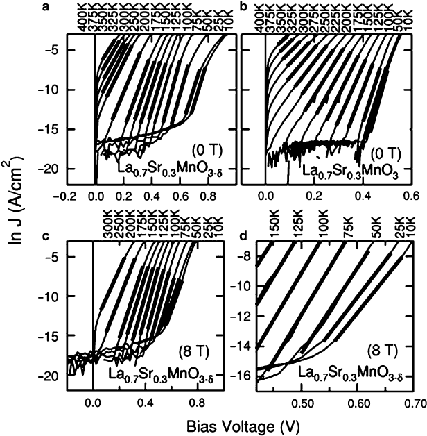
The relevance of the tunneling current (field emission) can be obtained by an-
alyzing the temperature dependent ideality factor. By fitting the semi-logarithmic
plot of the forward-biased I V characteristics at zero magnetic field for both
La
0:7
Sr
0:3
MnO
3•
and La
0:7
Sr
0:3
MnO
3
junctions (Figs. 5.23a, b), the plots of E
0
Fig. 5.23 Forward-bias I V characteristics for the (a)La
0:7
Sr
0:3
MnO
3•
and (b)La
0:7
Sr
0:3
MnO
3
junctions at 0 T. Characteristics for La
0:7
Sr
0:3
MnO
3•
junction at 8 T are shown in (c) and enlarged
in (d). The bold lines are linear fitting on a semi-logarithmic scale (From [103], by permission)
196 Y. Hikita and H.Y. Hwang
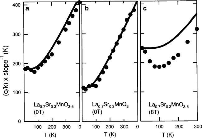
Fig. 5.24 Inverse of the slope in ln J–V plots (dots)andE
0
=k following (5.12)(curves)forthe
(a)La
0:7
Sr
0:3
MnO
3•
junction at 0 T, (b)La
0:7
Sr
0:3
MnO
3
junction at 0 T, and (c)La
0:7
Sr
0:3
MnO
3•
junction at 8 T (From [103], by permission)
vs. T are obtained shown in Fig. 5.24a, b. As evidenced by the good fit to the theoret-
ical curve (5.12), the junction transport in both cases can be described consistently
with the thermionic-field emission model.
By contrast, E
0
for the La
0:7
Sr
0:3
MnO
3•
junction measured under 8 T applied
magnetic field in Fig. 5.24c, obtained from Fig. 5.23c, d, shows a minimum in
E
0
vs. T below which E
0
increases again. Such behavior cannot be reproduced
by using (5.12) and thus requires an alternative explanation. Given this result,
the linear order magnetocapacitance and exponential junction magnetoresistance,
it can be concluded that the magnetic field reduces the Schottky barrier in the
La
0:7
Sr
0:3
MnO
3•
=NbWSrTiO
3
junction.
A similar case to La
0:7
Sr
0:3
MnO
3•
=NbWSrTiO
3
has been reported in Nd
0:5
Sr
0:5
MnO
3
=NbWSrTiO
3
junctions, in which a large negative junction magnetoresistance
is observed at low temperatures [99]. However, the Nd
0:5
Sr
0:5
MnO
3
thin film un-
dergoes an insulator-to-metal transition by application of magnetic field inducing a
change in the resistivity by more than six orders of magnitude, whereas in the case
of La
0:7
Sr
0:3
MnO
3•
the magnetoresistance of the film is of the order of 20%.
Other reports on junction magnetoresistance such as the cases of La
0:32
Pr
0:35
Ca
0:33
MnO
3
[95, 96]andLa
0:7
Ce
0:3
MnO
3
[97] exhibit both positive and nega-
tive magnetoresistance depending on the temperature. To clarify the origins for
these cases, recent focus has shifted more toward fundamental characterization of
the junctions such as the built-in potentials [104], junction current transport pro-
cesses [105], and detailed junction capacitance measurements [106].
5 Complex Oxide Schottky Junctions 197
Despite the remaining open questions regarding the origins for the various
types of junction magnetoresistance, manganite-titanate Schottky junctions offer a
new range of possible future applications using magnetic fields. Unlike the case
for magnetic tunnel junctions, here there is no spin selector, but rather a strong
charge-spin coupling directly modifying the “band diagram.” The quotation marks
indicate perhaps the central underlying question for many of the complex oxide
heterostructures, where the single-electron band picture is hardly applicable. Never-
theless, the ability to artificially engineer their interfaces gives access to many novel
physical properties in rectifying heterojunctions.
5.4.2 Carrier Density Tuning by Photocarrier Injection
Phase transitions induced by modulation of the carrier concentration are common
phenomena in perovskites, for which a method that can continuously vary the carrier
concentration is ideal. Up to now, metal–insulator (or ferroelectric)-semiconductor
field effect structures have been most extensively explored [107]. Under light illumi-
nation, Schottky junctions can also be used as flexible platforms for investigatingthe
doping dependence of perovskites, taking advantage of the strong internal electric
field for charge separation.
When light in excess of the energy gap of SrTiO
3
is illuminated on Schottky
junctions using NbWSrTiO
3
, electron-hole pairs are generated inside SrTiO
3
.The
electrons are swept away from the interface by the strong internal electric field,
whereas the holes are driven into the Schottky metal, hence selective hole doping
into the metal can be achieved. Using this technique, a number of examples modu-
lating the physical properties of the complex oxide thin films have been reported.
One of the early studies of photocarrier injection in perovskite heterostructures
is the report at the interface between La
1x
Sr
x
MnO
3
=SrTiO
3
,wherex 0:2.By
measuring the resistivity while illuminating with a Xenon lamp, a metal–insulator
transition was induced by photocarrier injection [108]. Note in this case the photo-
generating material was an undoped insulating substrate.
A series of experiments applying this technique have been undertaken by Mu-
raoka et al. The effectiveness of this method has been demonstrated in an induced
metal–insulator transition in La
0:7
Sr
0:3
MnO
3
=NbWSrTiO
3
and VO
2
=NbWTiO
2
[109],
and the modulation of T
c
in YBa
2
Cu
3
O
6C•
=NbWSrTiO
3
(Fig. 5.25)[110]and
Sr
0:89
Nd
0:11
CuO
2
=NbWSrTiO
3
[111]. In the case of VO
2
=NbWTiO
2
heterojunctions,
photoemission measurements under light illumination have also been carried out. By
comparing the open-circuit voltage with core-level shifts from PES, good agreement
was observed [112]. Further increase in the photo-injected carrier density has been
achieved by expanding the photocarrier generation region [113]. Figure 5.26ashows
the open-circuit voltage at different light intensity for two different concentrations of
Nb in LaMnO
3
=NbWSrTiO
3
heterojunctions. It is observed that the Nb D 0:01 wt%
heterojunction has a larger open-circuit voltage due to its longer depletion width
and higher efficiency in the spatial separation of the electron-hole pairs. To increase
the efficiency of the generation process, an additional insulating SrTiO
3
region was
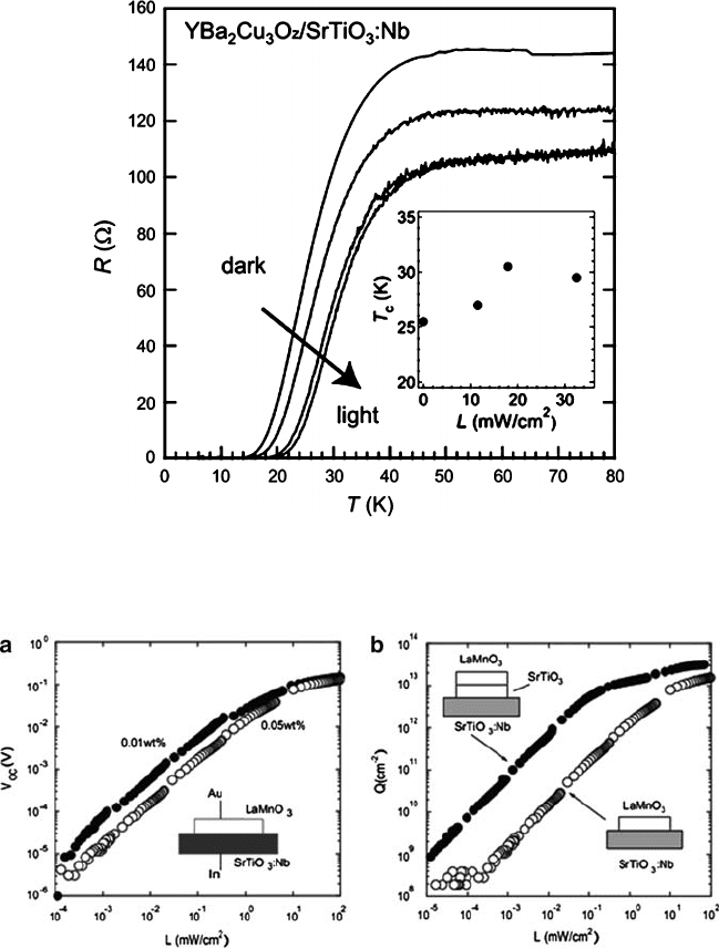
198 Y. Hikita and H.Y. Hwang
Fig. 5.25 Temperature dependence of the in-plane resistance of a YBa
2
Cu
3
O
6C•
thin film on
NbWSrTiO
3
.100/.Theinset displays the dependence of T
c
on light irradiance (From [110], by
permission)
Fig. 5.26 Light irradiance dependence of the (a) open-circuit voltage for LaMnO
3
=NbWSrTiO
3
for Nb D 0:01 wt% (solid circles) and 0.05 wt% (open circles). (b) Surface density of
holes injected to the film for LaMnO
3
=SrTiO
3
=NbWSrTiO
3
Nb D 0:05 wt% (solid circles)and
LaMnO
3
=NbWSrTiO
3
Nb D0:05 wt% (open circles)(From[113], by permission)
inserted between the LaMnO
3
thin film and the NbWSrTiO
3
substrate as can be seen
in Fig. 5.26b.
The advantage of this technique lies in the fact that the doping concentration of
the carriers is determined by the number of photons that are incident on the interface,
5 Complex Oxide Schottky Junctions 199
which enables simple and continuous tuning of the carriers. Compared with the
electric field effect in metal–insulator–semiconductor structures, this structure is
simply comprised of a single interface, and not limited by dielectric breakdown.
Although still at the conceptual level, the transparency of SrTiO
3
to the visible band
makes this technique a promising candidate for highly sensitive UV detectors if the
metal side can be switched between a highly metallic state to an insulating state by
the photo-injected electrons. Furthermore, addition of bias voltage tunability to the
heterostructure would enable electrochromic functionality in a simple structure by
selecting an appropriate material for the top metal.
5.4.3 Resonant Tunneling Through Metal-Induced
Interface States
Along with band bending and barrier heights, the formation of interface states
is an important concept in Schottky junctions, strongly influencing the junction
characteristics [40]. Intrinsic surface reconstructions, impurities or defects on the
semiconductor surfaces, or alloying by a metal–semiconductor reaction are typical
causes of the generation of interface states. In many cases, interface state formation
is driven predominantly by the properties of the semiconductor, and less dependent
on the properties of the metal, with some exceptions such as metal-induced-gap
states [44]. The chemical and structural similarities between metallic and semicon-
ducting perovskites enable the growth of epitaxial Schottky junctions. Furthermore,
upon doping impurities, many perovskite metals transit into a carrier localized state
long before completely establishing a gap. When interfaces are formed using such
disordered metals, a new type of interface state can be anticipated, which has been
explored in 5 at% Mn-doped SrRuO
3
=NbWSrTiO
3
Schottky junctions [114]. By par-
tial doping of Mn in SrRuO
3
, a metal–insulator transition is induced at Mn D 0:4
[115]. At x D 0:05; SrRu
1x
Mn
x
O
3
is a metal with a slightly increased resistivity.
The temperature dependent I V characteristics for SrRuO
3
=NbWSrTiO
3
and
SrRu
0:95
Mn
0:05
O
3
=NbWSrTiO
3
are shown in Fig. 5.27a, b, respectively.
In the case of the SrRuO
3
junction, the forward-bias current in the semi-
logarithmic plot is linearly proportional to the bias voltage with an overall shift
to higher voltages at lower temperatures, indicating typical Schottky behavior. The
current transport mechanism of these junctions was determined to be thermionic-
field emission crossing over to field emission at low temperatures. By contrast,
the I V characteristics of the SrRu
0:95
Mn
0:05
O
3
=NbWSrTiO
3
junction (Fig. 5.27b)
exhibit a large reduction in the current density over the measured voltage range, and
a current peak and negative differential resistance (NDR) appear at forward-bias
below 60 K. Since the NDR behavior is observed in the field-emission low temper-
ature region, Mn substitution appears to induce a resonant state similar to a double
barrier resonant tunneling diode [116], as illustrated in Fig. 5.28.
To verify the role of Mn doping on the NDR, I V characteristics were studied
in a series of modulated heterointerfaces where the position of the Mn impurity was
varied across the interface. The resonance peak was only observed for Mn just on
