Paulo D.J. Surface Integrity in Machining
Подождите немного. Документ загружается.

4 Characterization Methods for Surface Integrity 131
P
s
and Z-axis). A uniformly illuminated non-transparent isotropic surface is assumed
for this technique, so BSDF is not applicable for the anisotropic surface [4, 5].
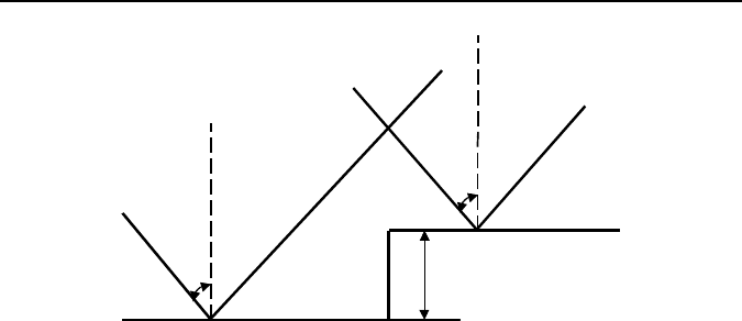
The third technique commonly used for surface analysis is the speckle contrast
measurement. When coherent light illuminates the rough surface, the reflected
beam accounts for part of the random patterns of bright and dark regions known as
“speckle”. The speckle pattern is created by the interference of wavelets scattered
from points of different heights within the illuminated area (as shown in Fig-
ure 4.6, where v is the angle of illumination and h the height of the roughness) [6].
In the speckle contrast measurement, the average contrast, defined as the normal-
ized standard deviation of intensity variations at the observed surface, has a strong,
linear correlation with the surface roughness parameter R
a
[7, 8].
4.1.3 Scanning Probe Microscopy Technologies
In scanning probe microscopy technologies, the surface can be measured and im-
aged to a very fine scale, down to the molecular level. Scanning tunneling micros-
copy (STM) and atomic force microscopy (AFM) are the major two types of scan-
ning probe microscopy methods.
Figure 4.7 illustrates the working mechanism of STM. The basic idea is to bring
a fine metallic tip close (a few Å) to a conductive sample. By applying a voltage
between the tip and the sample, a small electric current (0.01–50 nA) can flow
from the sample to the tip or reverse, which is called electronic tunneling. The
exponential relationship between the tunneling current and the distance from the
tip to the sample results in high vertical resolution.
By scanning the tip across the surface and detecting the current, the surface to-
pography can be generated with very fine resolution. The lateral resolution is about
1
Å, whereas a vertical resolution up to 0.01
Å can be achieved. The STM can be
used in ultrahigh-vacuum, air or other environments.
The STM is widely used for surface analysis. It can be used to study metals and
semiconductor surface, especially semiconductors used in microelectronics fabrica-
tion. It can also be used to study microtopography and nanotopography of the sur-
face on high-precision components. The major limitation of STM is that STM can
h
ν
ν
Figure 4.6. Difference caused by surface roughness (after [7])
132 J. Zhang and Z.J. Pei
only be used for conductive or semiconductive surfaces. The resolution of me-
chanical components will depend on the ability to move the tip precisely and
measure its position accurately [9−11].
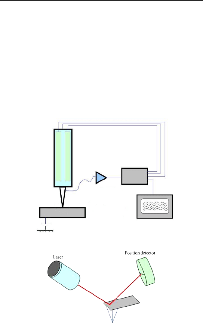
In AFM, almost any type of surfaces, including polymers, ceramics, composites,
glass, and biological samples can be characterized. A fine ceramic or semiconduc-
tor tip scans the sample surface, the tip is positioned at the end of the cantilever
beam and as the tip is attracted or repelled, the deflection is captured by a laser
reflecting at an oblique angle from the tip of the cantilever and the plot of laser
deflection versus tip position on the sample provides the topography of surface, as
shown in Figure 4.8.
A sharp probe is positioned close enough to the surface so that it can interact
with the force fields associated with the surface. Then the probe is scanned across
the surface in such a way that the forces between the probe and surface remain
Figure 4.7. Illustration of STM (after [9])
Figure 4.8. Illustration of beam deflection system by using a laser and photo detector to
measure the beam position in AFM (after [12])
Control voltages for piezotube
Distance control
and scanning unit
Data processing
Tunneling voltage
Sample
Piezoelectric tube with electrodes
Tunneling
Current amplifier
4 Characterization Methods for Surface Integrity 133
constant. By monitoring the precise motion of the probe when it is scanned over
the surface, the topography of the surface can be constructed. The force on the
probe is controlled by the feedback from the deflection of the laser beam on to
the position detector. Magnifications of the AFM may be from 100 times to
100,000,000 times in the horizontal (x−y) and vertical axis [12].
4.2 Microstructure Characterization Technologies
4.2.1 X-ray Diffraction
X-ray diffraction is widely used as a non-destructive method to determine crystal-
line structure and residual stress from the lattice deformation of a crystal. A crystal
lattice is a regular three-dimensional distribution (cubic, rhombic, etc.) of atoms in
space. When X-rays come in at a particular angle, they are reflected specularly
(mirror-like) from the different planes of crystal atoms. However, for a particular
set of planes, the reflected waves interfere with each other. A reflected X-ray sig-
nal is only observed if Bragg’s condition is met for constructive interference.
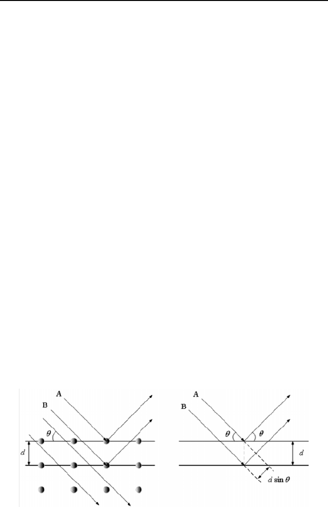
Figure 4.9 illustrates how X-ray diffraction works. Figure 4.9(a) shows X-rays
incident upon a simple crystal structure, Bragg’s condition is met for both ray A
and ray B. Figure 4.9(b) shows the diffraction geometry.
The extra distance travelled by ray B must be an exact multiple of the wave-
length of the radiation. This means that the peaks of both waves are aligned with
each other. Bragg’s condition can be described by Bragg’s Law: 2dsin
θ
=m
λ
,
where d is the distance between planes,
θ
is the angle between the plane and the
incident (and reflected) X-rays, m is an integer called the order of diffraction and
λ
is the wavelength [13, 14].
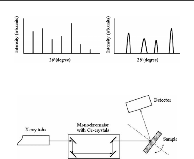
Figure 4.10(a) shows a standard X-ray diffraction pattern with aligned sharp
peaks for a perfect crystal structure. During machining processes, residual stress
may be resulted from non-uniform, permanent three-dimensional changes in the
material. These changes usually occur as plastic deformation and may also be
(a) (b)
Figure 4.9. Illustration of X-ray diffraction: (a) X-rays A and B incident upon a crystal, and
(b) diffraction geometry (after [14])
134 J. Zhang and Z.J. Pei
caused by cracking and local elastic expansion or contraction of the crystal lattice
[15]. In these cases, the crystal structure is no longer perfect (d is changed) and the
diffraction peaks are broadened and shifted, as shown in Figure 4.10(b). Thus, by
examining the changes of the X-ray diffraction pattern, the residual stress can be
characterized.
For the applications of conventional X-ray diffraction, the main restriction is the
low penetration depth of X-rays into the workpiece material. Because the strain can
only be measured within the irradiated surface layer, with low penetration depth of
X-rays, only the stress close to the surface can be detected quantitatively. Tonshoff
et al. [16] used a high-resolution X-ray diffractometer (shown in Figure 4.11) to
detect the damaged layer of machined silicon wafers.
This diffractometer consists of a four-crystal monochromator that produces a
highly parallel and monochromatic incident beam so that a high resolution of X-ray
diffraction can be achieved.
4.2.2 Electron Diffraction
Electron diffraction is similar to a regular microscope. The major difference is
that, instead of a light beam, an electron bean is utilized in order to be able to
visualize small objects (of the order of nanometers). This electron beam is directed
(a) (b)
Figure 4.10. Illustration of X-ray diffraction patterns: (a) for a perfect crystal; and (b) for an
imperfect crystal (after [14])
Figure 4.11. Illustration of high-resolution X-ray diffraction system (after [16])
4 Characterization Methods for Surface Integrity 135
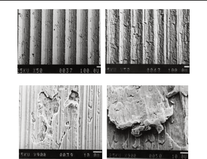
(a) (b)
(c) (d)
Figure 4.12. A Influence of cutting speed in turned surfaces: (a) cutting speed of 283 m/min
under 50×, (b) cutting speed of 71 m/min under 50×, (c) cutting speed of 283 m/min under
900×, (d) cutting speed of 71 m/min under 900× [17]
and focused to the tested surface. In scanning electron microscopy (SEM), when
the electron beam is incident on the surface, the electron will be refracted by the
surface, therefore, the surface of the material will be detected; transmission elec-
tron microscopy (TEM) is the reflection of the electrons that passes through the
specimen, therefore the crystal structure of the specimen can be detected. Com-
pared with the traditional microscopes, the SEM has many advantages, including a
larger depth of field and much higher resolution [18].
Under SEM, it is possible to observe the influence of cutting speed on the sur-
face finish of turned surfaces in steel AISI 12L13, which is shown in Figure 4.12.
The turning tool used is cemented carbide P10; feed rate employed is 0.25
mm/rev;
depth of cut is 0.5
mm.
4.2.3 Cross-sectional Microscopy
For the cross-sectional microscopy method, the tested samples must be appropri-
ately prepared, before observation under an optical microscope. Normally, the
sample preparation consists of four general steps [1]: cleaving, sanding, polishing
and etching. (1) Cleaving is done perpendicularly to the machined surface. (2) The
136 J. Zhang and Z.J. Pei
surface of the cleaved sample is wet-sanded to remove enough material from the
cross-section of interest to ensure that any damage incurred during cleaving is
removed. (3) The test surface is refined by polishing. The polished surface should
also be maintained flat and perpendicular to the machined surface. (4) The test
surface is placed into “Yang” solution [19] (H
2
O: HF49%: Cr
2
O
3
= 500
ml: 500
ml:
75
g) for 5
s at room temperature, which will make the microstructure more dis-
cernible for microscopy observation. The sample preparation process is very criti-
cal to obtain the true signal.
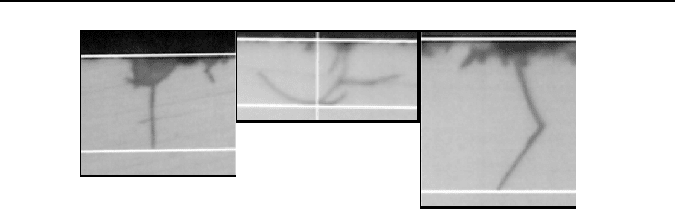
Cross-sectional microscopy can also be used to assess the subsurface damage,
providing information about the subsurface damage depth and subsurface damage
distribution. But the sample preparation process is tedious. If not properly done,
the sample preparation process itself will generate damage.
Using cross-sectional microscopy technology, the subsurface cracks in silicon
wafers machined by various mechanical processes have been studied and the re-
sults of subsurface cracks, including crack configurations and crack depth are
shown in Figure 4.13.
4.3 Elementary Analysis Technologies
4.3.1 X-ray Fluorescence
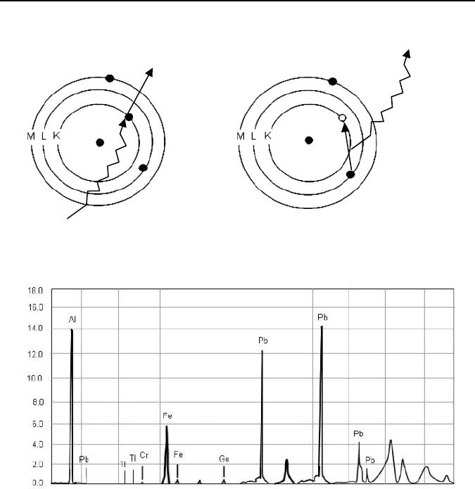
X-ray fluorescence, also known as (XRF) is the reaction from the electrons to the
X-rays. The X-rays excite the electrons and they “jump” from the inner shell to an
outer one. When the electron jumps, it leaves a vacancy and that vacancy is imme-
diately filled by another electron. The “reaction” of the electron jumping from one
shell to another is called fluorescence. Figure 4.14 shows graphically the definition
of XRF [20, 21].
A typical result obtained from XRF analysis is shown in Figure 4.15. The ele-
ments that show higher peaks are the ones that have a major concentration in the
material. In this example, the predominating elements are lead and aluminum.
Other elements that also have been detected are chromium, iron, and titanium, but
their concentration is not significant [20, 21].
(a)
(b)
(c)
Figure 4.13. Crack configurations and depth in ground silicon wafers: (a) depth of 15.9
μm,
(b) depth of 8.2
μm, (c) depth of 19.9
μm
4 Characterization Methods for Surface Integrity 137
Emitted X-ray is detected
by the detector
Photon or X-ray
Electron from outer shell
fills the hole
Core electron lifted into
the continuum
Figure 4.14. Illustration of XRF (after [21])
Figure 4.15. Results of XRF analysis (after [21])
4.3.2 Others
Energy-dispersive X-ray spectroscopy (EDS, EDX or EDXRF) is another analyti-
cal technique used for the elemental analysis of a sample. Sometimes EDX is used
in conjunction with SEM.
The fundamental principle of EDX characterization capability is that each ele-
ment has a unique atomic structure, therefore allowing X-rays characteristic of an
element’s atomic structure to be identified uniquely from each other. The X-ray
characteristic is the energy absorption that will produce electron movements be-
tween orbital on the atom, therefore emitting X-rays. This emitting X-ray together
with the amount of energy submitted will determine the element that is being
scanned [22].
Auger electron spectroscopy (AES) can also be used to determine the chemical
composition of the tested surface, and it can be applied to all solid materials, in-
cluding polymers and glasses. Underlying the spectroscopic technique is the Auger
138 J. Zhang and Z.J. Pei
effect, which is based on the analysis of energetic electrons emitted from an ex-
cited atom after a series of internal relaxations.
In general, AES is able to analyze the furthest two through ten atomic layers of
the surface. However, if the interested region is below the surface, ion etching can
be used to remove the topmost atomic layers. For the detailed information about
ion etching, please refer to [23].
AES and X-ray photoelectron spectroscopy (XPS, presented in Section 4.4.1)
give similar information, but the Auger spot size is much smaller than the XPS one,
therefore, having the capability of identifying very fine features on the surface.
4.4 Chemical Composition Analysis Technology
X-ray photoelectron spectroscopy (XPS) is also known as electron spectroscopy for
chemical analysis (ESCA). It is a surface analysis technique where a sampling vol-
ume that extends from the surface to a depth of approximately 50−70
Å can be ana-
lyzed. It is used to determine quantitatively elemental states in the material, and
provide chemical composition of the detected elements within the material. Compo-
sition depth profiling can be achieved by using an ion beam to sputter etch the sam-
ple between analysis cycles.
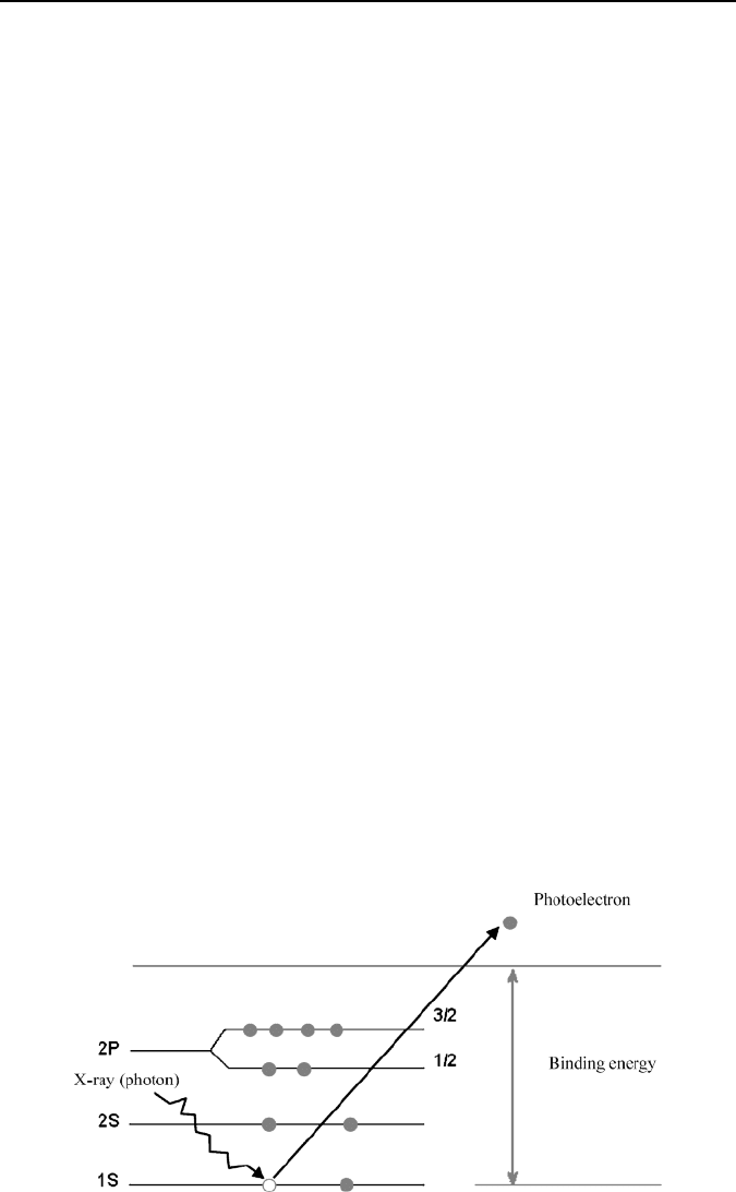
The working principle of XPS is shown in Figure 4.16. When the tested sample is
irradiated by the monochromatic X-rays, the photoelectrons whose energies are char-
acteristic of the elements within the sampling volume will be emitted. Therefore, by
detecting small shifts in the atomic binding energies of the photoelectrons, the
chemical states of the elements can be determined. The fundamental principle is that
the core electronic levels of the binding energies are uniquely different for each spe-
cific element in the material, so elemental analysis can be obtained from the spectra.
All elements except hydrogen and helium are detectable from XPS. The intensity of
the peaks on the spectra is related to the concentration of the element within the tested
region. Also, small shifts in element binding energies (commonly referred as the
chemical shifts) provide information about the chemical state of the element, which
are due to the modification of the electronic levels caused by changes [24−26].
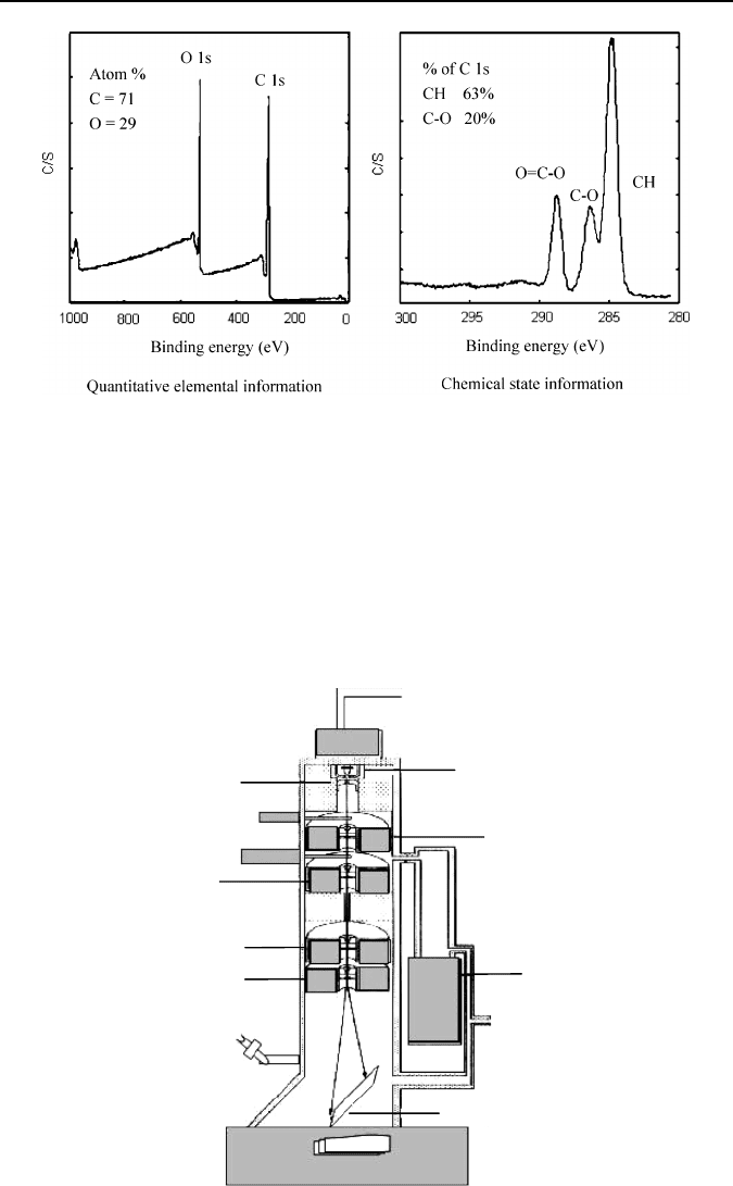
Figure 4.17 shows the XPS spectra results on polyethylene terephthalate [27].
Figure 4.16. Basic principle of XPS (after [24])
4 Characterization Methods for Surface Integrity 139
Figure 4.17. XPS results of polyethylene terephthalate (after [27])
4.5 Microcrystalline Structure and Dislocation Density
Characterization Technology
Transmission electron microscopy (TEM) is a microscopy technique used to char-
acterize the microstructure of materials with very high spatial resolution. Informa-
tion about the morphology, crystal structure and defects, crystal phases and com-
position can be obtained from TEM.
High voltage source
Electron gun
Condenser lens
Turbo pump
To rotary pump
Screen
Plate camera
Anode
Condenser aperture
Specimen airlock
Projector lenses
Viewing scope
Viewport
Figure 4.18. Illustration of TEM (after [28])

140 J. Zhang and Z.J. Pei
In TEM, a beam of electrons is transmitted through a very thin specimen, inter-
acting with the specimen when they pass through the specimen. Then the electrons
are focused with electromagnetic lenses and the image is observed on a fluorescent
screen, or recorded on film or digital camera. Compared with the light used in the
optical microscope, the electrons are accelerated at several hundred kV, giving
wavelengths much smaller than that of light: 200 kV electrons have a wavelength
of 0.025
Å. However, the resolution of TEM is limited by the aberrations inherent
in electromagnetic lenses, to about a few angstroms.
References
[1] Stephenson D.A., Agapiou J.S., (1996) Metal Cutting Theory and Practice, Marcel
Dekker, New York
[2] Davies H., (1954) The Reflection of Electromagnetic Waves from a Rough Surface,
Proc. Inst. Elec. Eng., Vol. 101, pp. 209
[3] Vorburger T.V., Teague E.C., (1981) Optical Techniques for On-Line Measurement
of Surface Topography, Precision Engineering, Vol. 3, No. 2, pp. 61−83
[4] Stover J.C., (1990) Optical Scattering Measurement and Analysis, McGraw-Hill, New
York
[5] Nicodemus F.E., Richmond J.C., Hsia J.J., Ginsberg I.W., Limperis T., (1977) Geo-
metric Considerations and Nomenclature for Reflectance, NBS Monograph 160, U.S.
Dept. of Commerce, Washington, DC
[6] Persson U., (1992) Real Time Measurement of Surface Roughness on Ground Sur-
faces Using Speckle-contrast Technique, Optics and Lasers in Engineering, Vol. 17,
No. 2, pp. 61−67
[7] Asakura T., (1978) Surface Roughness Measurement, Speckle Metrology, ed. Erf
R.K., Academic Press, New York
[8] Fujii H., Asakura T., (1974) Effect of Surface Roughness on the Statistical Distribu-
tion of image Speckle Intensity, Optics Communications, Vol. 11, No. 1, pp. 35−38
[9] Bai C., (1992) Scanning Tunneling Microscopy and its Application, Springer Verlag,
Berlin
[10] Guntherodt H.J., Wiesendanger R., (1991) Scanning Tunneling Microscopy I-III,
Springer Verlag, Berlin
[11] Stroscio J.A, Kaiser W.J., (1993) Scanning Tunneling Microscopy, Academic Press
[12] Online: Atomic Force Microscope, http://www.nanoscience.com/education/AFM.html
[13] Hecht E., (2002) Optics, 4th edn., Addison Wesley , New York
[14] Online: Limits of Resolution: X-ray Diffraction, http://physics.bu.edu/py106/notes
[15] Bismayer U., Brinksmeier E., Guttler B., Seibt H., Menz C., (1994) Measurement of
Subsurface Damage in Silicon Wafers, Precision Engineering, vol. 16, pp. 139−143
[16] Tonshoff H.K., Schmieden W.V., Inadaki I., Konig W., Spur G., (1990) Abrasive
Machining of Silicon, Annals of the CIRP, vol. 39 no. 2, pp. 621−630
[17] Davim J.P. (1991) Influência das condições de corte na microgeometria das super-
fícies obtidas por torneamento, MSc thesis, University of Porto, Porto (in portuguese)
[18] Online: The Microscopy Facility, http://bioweb.usu.edu/microscopy/
[19] Yang K H., (1984) An Etch for Delineation of Defects in Silicon, Journal Electrome-
chanical Society, Solid State Science and Technology, Vol. 131, No. 5, pp. 1140−1145
[20] Lachance G.R., Claisse F, (1995) Quantitative X-ray Fluorescence Analysis: Theory
and Application, Wiley, Chichester