Marulanda J.M. (ed.) Electronic Properties of Carbon Nanotubes
Подождите немного. Документ загружается.

Carbon Nanotube Based Magnetic Tunnel Junctions (MTJs) for Spintronics Application
505
(7)
Since
2
i
E
v
hk
, the positive current can be expressed as
(8)
where h is the Planck’s constant and
i
is the cutoff energy of the i subband. The negative
current is similarly given by
(9)
and the total current as
(10)
(11)
is the number of modes in subband i having energy less than E, and u is a Heaviside
function. Low temperature has been assumed so that
(−)≈(−) and M has been
assumed to be constant in the energy range
21
. (12)
The total current density will be calculated by adding current of each spin channel,
I = I↑ + I↓ (13)
and the spin current is given by the difference between up spin and down spin currents.
The introduction of a 3D system can further increase the consistency of calculation
compared to 1D.
In this review, we emphasis on graphene and CNTs based MTJs which are the most recent
attractions in MTJ research.
5. Graphene based MTJs
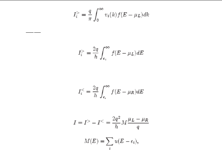
Graphene is the building block of graphite and it is made from a hexagonal lattice of carbon
atoms with sp
2
bonds (Figure 7). Graphene is a promising material for spintronics and MTJs
due to its intrinsic spin orbit interaction [79-87]. The electron spin of graphene also has
interaction with the carbon nuclei. In addition, its unique properties, especially long spin
flip length up to 1μm at room temperature enhances its potential to spintronics. They also
show half integer quantum hall effect and high electrical conductivity. Many groups have
studied TMR for graphene connected to ferromagnetic leads. They have demonstrated
injection of spin polarized current in the system. Graphene is ideal for application of spin
Electronic Properties of Carbon Nanotubes
506
valve effect in which the resistance of the devices can be changed by manipulating the
relative orientation of the magnetization. Hill et al [88] fabricated a spin valve device
consisting of a graphene connected by two FM leads and investigated a 10% change in
resistance as the electrodes switch from parallel to antiparallel state.
Fig. 7. Graphene showing the 2-D network of sp
2
bonded carbon atoms.
Experimentally, there have been few evidences for spin-polarized transport in graphene
spin valves [89]. Wang et al investigated the magnetoresistance (MR) properties of quasi-
two-dimensional mesoscopic graphite (MG) spin valve devices consisting of flakes with
thickness between 1 and 40 nm (3 to 100 layers of graphene) contacted by two ferromagnetic
electrodes and observed signatures of spin-polarized transport for MG flakes in the
thickness range 10–40 nm. For devices in which an ultrathin magnesium oxide (MgO)
tunnel barrier is inserted at the FM/MG interface, the spin valve effect has been observed
with MR magnitudes up to 12% at 7 K and signals persisting up to temperatures as high as
60 K. In contrast, the spin valve effect has not been seen in devices without MgO, suggesting
the importance of spin-dependent interfacial resistance for spin injection into MG [90-92].
Investigation of the voltage bias dependence of the MR finds a reduction of the MR with
increasing voltage and a correlation with the differential conductance. Finally, the spin valve
signal exhibits oscillatory MR as a function of gate voltage [93-95].
Carbon Nanotube Based Magnetic Tunnel Junctions (MTJs) for Spintronics Application
507
6. Carbon nanotubes based MTJs
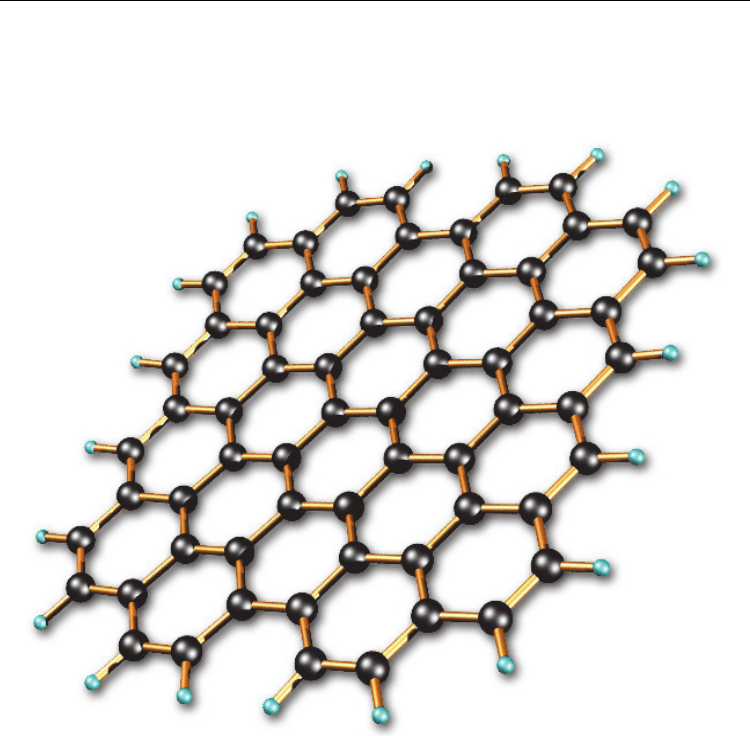
Carbon nanotubes (CNTs) [96] are molecular tubes of carbon with outstanding properties
(Figure 8). They are among the stiffest and strongest materials known, and have remarkable
electronic behaviour and many other unique properties. They are attractive for spintronic
devices due to their nanoscale size, extremely large spin flip scattering lengths and because
they can behave as one-dimensional ballistic quantum conductors [97-102]. Experimental
investigations on coherent spin transport through Co-contacted CNTs showed that spin can
be coherently transported over 130 nm through the carbon nanotube [103].
Fig. 8. Image of a carbon nanotube.
6.1 Fabrication of vertically aligned carbon nanotubes
Various conventional methods have been used to grow CNTs, including arc-discharge, laser
ablation, and chemical vapor deposition (CVD). However, only chemical vapour deposition
(CVD) methods allow the controlled growth directly on a substrate, which is important for
many applications, especially as the individual manipulation of CNTs is difficult and
expensive, due to their reduced size. The orientation of CNTs is highly important in
achieving the maximum benefit of its property. The ability to pattern or position carbon
nanotubes (CNTs) with a vertical orientation in controlled arrays has been demonstrated by
many researchers
[104-106]. Conventional plasma enhanced (PE) CVD is an established
technique for the synthesis of vertically aligned CNTs[107-110]. Selective, aligned growth of
CNTs on silicon and glass substrates has been demonstrated by plasma enhanced chemical

Electronic Properties of Carbon Nanotubes
508
vapor deposition. However, despite the high level of control, PECVD growth typically
involves processing temperatures over 900 ºC, which significantly limits the choice of the
possible substrate materials and the integration processes. Bonard et al
6
have demonstrated
in their work that the enhanced field emission factors of individual CNTs (30 000-50 000) are
very large, when compared to the CNT films (1000-3000) [111-112]. The smaller field
emission factors in the CNT film have been considered a consequence of the effect of the
planar substrate supporting the CNT film. The field-enhancement factors of dense CNT
films were even smaller because the electric field on one tube is screened by the proximity of
neighboring tubes.
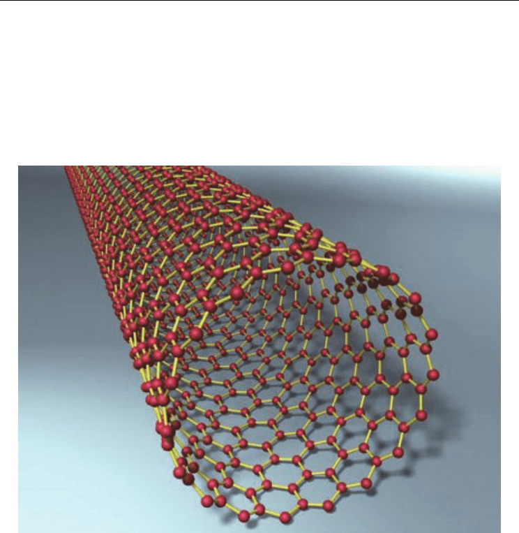
We reported the selective growth of VACNTs on large area copper substrates using a
double plasma hot-filament chemical vapour deposition system (DP-HFCVD) [JNN paper
113]. We employed our modified HF-CVD system (Figure 9) for the deposition of large area
(1-1.5 inch
2
) carbon nanotubes onto nickel electroplated copper substrates. The system
employed three independent power supplies, which were used to generate two independent
plasma glow discharges within the vacuum chamber. The system consisted of two parallel
molybdenum plates sandwiching a resistive tantalum filament. Each of the two
molybdenum plates was electrically biased, either positively or negatively, with respect to
the filament, in order to generate the two glow discharges. The precursor gases used were
methane and hydrogen (gas flow: 46/200 sccm) at 7 mbar. The DC voltage (0-600 V) was
applied between the upper substrate electrode and the filament. The filament power was
maintained at 600 W and the substrate temperature (650 ºC) was measured using a sealed
thermocouple placed inside the substrate holder immediately beneath the substrate.
The growth of the CNTs involves three processes: (i) substrate pretreatment, (ii) nucleation
and (iii) the actual growth of the CNTs.
(i) A 0.8 mm thick flat copper substrate with 98% purity was treated by sand blasting and
then cleaned in ultrasonic acetone bath. The cleaned substrate was subsequently
electroplated with nickel in a nickel sulphate bath. The copper substrates were used as the
cathode and a nickel rod served as the anode. The 50 nm nickel coated copper substrates
were subsequently transferred to the HF-CVD chamber and the chamber was purged by
100 sccm hydrogen gas for a few hours.
(ii) For the nucleation, the substrates were exposed to hydrogen plasma, promoting the
etching of the catalyst and enabling the formation of nickel nano-clusters.
(iii) Finally, the CNTs were grown with hot filament power in the presence of precursor
gases, methane and hydrogen.
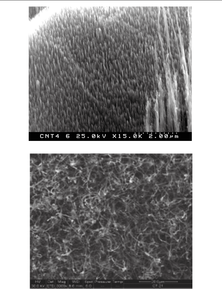
The morphology of the CNTs deposited at different times was examined using SEM
microscopy. Figure 10 shows the SEM image of CNTs deposited by DP-HFCVD (a) and
conventional CVD (microwave) (b) in 2 hours. Unlike the conventional CVD CNTs, the DP-
HFCVD CNTs appeared highly dense and were grown perpendicular to the substrate. It is
reported that the growth rate in plasma enhanced (PE)CVD is generally slower than that in
thermal CVD, which may be partly due to the atmospheric pressure operation of thermal
CVD
[114]. The CNTs grown by DP- HFCVD system also showed a slow growth rate and,
taking almost 2 hours to form a forest of tubes. Bower et al [115] showed the effect of the
electric field on the alignment of nanotubes unambiguously in a microwave plasma of
acetylene and ammonia. Initially, when the plasma was on, their multiwalled (MW) CNTs
were vertical; when growth proceeded with plasma off (in a thermal CVD mode), the
nanotubes were found to be curly or randomly oriented. They also found that nanotubes
Carbon Nanotube Based Magnetic Tunnel Junctions (MTJs) for Spintronics Application
509
always grew perpendicular to the substrate surface regardless of the substrate position or
orientation. Since their work, a number of articles have appeared, considering the general
orientation of PECVD-grown nanotubes better than the results from thermal CVD
[116].
However, all these works were concentrated only on vertical alignment of the tubes, and the
adherent properties of the tubes were ignored.
Fig. 9. Computer drawing of DP- HFCVD system.
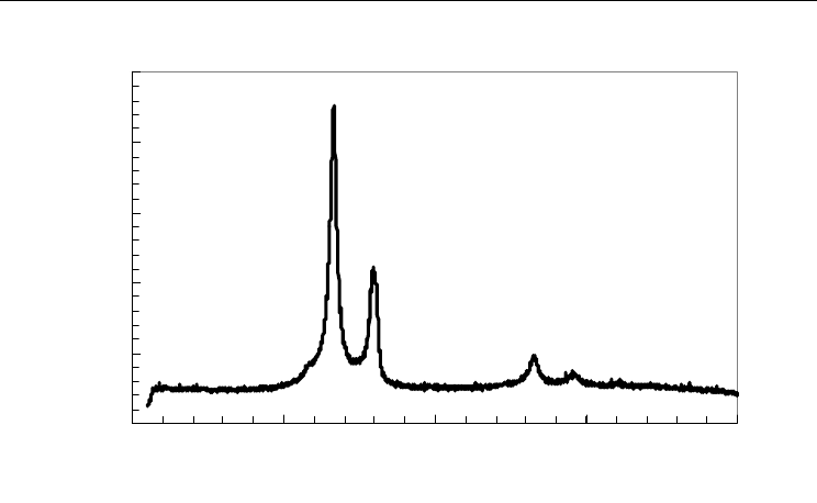
The quality of the CNT was confirmed by Raman Spectroscopy. Figure 11 shows the micro-
Raman spectra for samples (a) VACNT and (b) conventional CVD. The most prominent
features in the first-order Raman spectra were observed for both the samples positioned at
around 1570cm
-1
(G band) and 1350cm
-1
(D band). The peaks positioned at 1350 cm
-1
represent the disorder-induced phonon mode (D-band) and the strong peak at 1577 cm
-1
(G-
band) can be assigned to the Raman-allowed C-C phonon mode (E2g-band) [117]. A small
difference in the D and G peak positioning was noted with these samples and we attribute
this to the structural differences in the tubes.
Electronic Properties of Carbon Nanotubes
510
(a)
(b)
Fig. 10. SEM images of CNTs deposited by (a) DP-HFCVD and (b) Conventional CVD
(micro-wave) in 2 hours.
Carbon Nanotube Based Magnetic Tunnel Junctions (MTJs) for Spintronics Application
511
0
500
1000
1500
2000
2500
0 1000 2000 3000 4000
Fig. 11. Micro-Raman spectra of VACNT.
6.2 TMR in CNT based spintronic devices
Since its discovery, a large number of nanodevices such as single electron transistor, Light
emitting diode, field effect transistor has been demonstrated. However, these devices are
based on charge of the electron. TMR characteristics have already been measured in CNTs
both experimentally and theoretically [118]. K Tsukagoshi et al [103] demonstrated the MR
in a single CNT contacted by ferromagnetic metal electrodes. The spintronic devices
exhibiting TMR using ferromagnet-contacted single walled carbon nanotubes (SWCNTs)
have been demonstrated by A. Jensen et al [118]. Most of the reports on CNT-TMR system
are mainly based on single carbon nanotube contacted to bulk ferromagnetic material by an
ex-situ method [119-121]. The TMR effect is also known to be sensitive to the tunnel
barrier/electrode interface. The barrier sensitivity may be more evident in a system with
single CNT. De Teresa et al [122] studied ferromagnetic MTJ with various barrier materials
and found that even the sign of the TMR depends on the barrier materials. S. Yuasa et al
[123] also investigated the effect of crystal anisotropy of the spin polarisation on MTJ using
single crystal iron electrodes of various crystal orientations. They found a clear crystal
orientation dependence of the TMR which might reflect the crystal anisotropy of the
electronic states in the electrodes.
The current authors followed a different approach for the development of a potential MTJ
device. The details are discussed below.
Figure 12 shows the Field-Emission Scanning Electron Microscopy (FE-SEM) image of the
MTJ system fabricated by the current authors. The Ni nanoparticles (on top, ~1µm in
thickness) deposited on top of the VCNTs are apparent in figure 12. High density well
aligned MWCNTs with length larger than 2 µm are apparent in the image. The details of the
substrate pre-treatment method, the formation of nanoclusters and the synthesis of
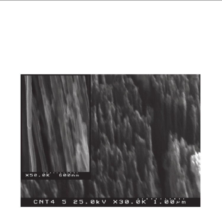
Electronic Properties of Carbon Nanotubes
512
vertically aligned MWCNTs on nickel plated copper substrate using a double plasma
method is reported in our previous paper [124].
Energy Dispersive X-ray microanalysis
(EDS) attached to the FE-SEM reveals Ni nanoparticle deposition on the top surface of
VCNTs. The magnified FE-SEM images of the green dashed square areas marked by 1 and 2
in Figure 12 are illustrated in inset. Unlike CNTs grown by conventional techniques,
VCNTs grown by DP-HFCVD technique are short (~ 2μm), isolated and vertically aligned to
the substrate. The green dotted square area 1 illustrates the VCNTs covered by nano nickel
paticle. However, the particles are less in the lower portion of the sample (Green dashed
square area 2).
Fig. 12. FE-SEM image of the VCNT sample deposited with nickel nanoparticles. The inset
shows a magnified FE-SEM image displaying isolated VCNTs.
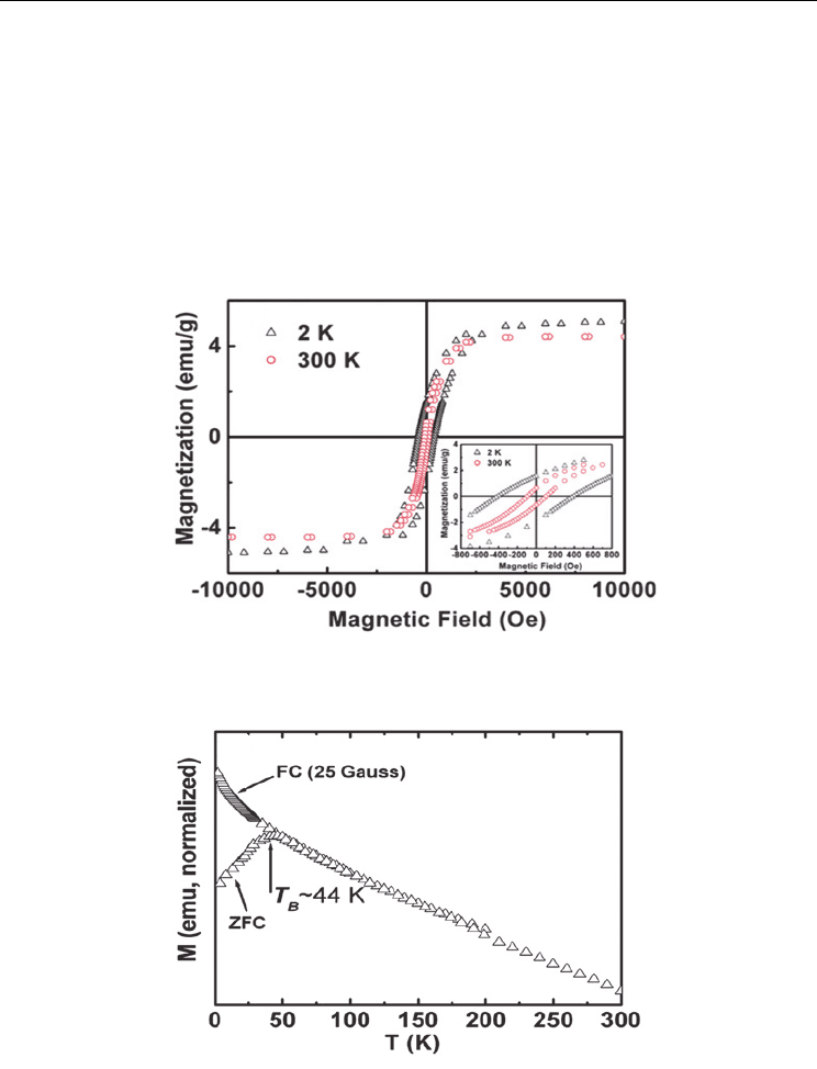
TMR/GMR is known to originate from spin interaction between the magnetic and
nonmagnetic particle at the interface and are related to the coercivity value [125]. To probe
the magnetic properties, the field dependence of the magnetization was measured using a
superconducting quantum interface device (SQUID) [126]. Figure 13a shows magnetization
vs. applied magnetic field for nickel nanoparticle deposited VCNTs at 2 K and 300 K,
respectively. It indicates that the sample exhibits ferromagnetic behaviour with a hysteresis
loop at 2 K and 300 K, respectively. The saturation magnetization (M
s
), coercivity (H
c
), and
remnant magnetization (M
r
) for both temperatures are summarized in Table 1. The
saturation magnetization values and coercivity for nickel nanoparticle deposited VCNTs
shows a decrease from 5.3 to 4.4 emu g
-1
and 395 to 115 Oe, respectively, with the increase of
temperature, indicating a characteristic ferromagnetic behaviour. To gain a better
understanding of the magnetic behaviour of nickel nanoparticle deposited VCNTs, we have
performed zero-field-cooled (ZFC) and field cooled (FC) magnetization measurements. For
Carbon Nanotube Based Magnetic Tunnel Junctions (MTJs) for Spintronics Application
513
the ZFC measurement, the nickel nanoparticle deposited VCNTs sample is first cooled from
300 to 2 K in zero magnetic field. On the other hand, for FC measurements, the sample is
cooled in the magnetic field (25 Gauss) from 300 to 2 K, and later the magnetization is
measured in the warming cycle keeping the field on. Figure 13b shows the temperature
dependence of ZFC and FC measurements under the applied magnetic field of 25 Gauss for
nickel nanoparticle deposited VCNTs which exhibits the main features of ferromagnetic
behaviour [127]. The blocking temperature T
B
(transition temperature from ferromagnetic to
superparamagnetic state) peak can be observed in ZFC curve at about ~44 K. The low value
of T
B
is directly in agreement with smaller size of nickel nanoparticles randomly deposited
on the VCNTs [128,129].
Fig. 13. (a) Magnetization vs. applied magnetic field for nickel nanoparticles deposited
VCNTs at 2 K and 300 K. The ferromagnetic behaviour of the sample is apparent from the
hysteresis (b) Temperature dependence of ZFC and FC measurements under the applied
magnetic field of 25 Gauss for nickel nanoparticle deposited VCNTs.
a
b
Electronic Properties of Carbon Nanotubes
514
T/K M
s
/emu g
-1
H
c
/Oe M
r
/emu g
-1
2 5.3 395 1.6
300 4.4 115 0.6
Table 1. M
s
, H
c
, M
r
for Ni nanoparticle deposited VCNTs at 2 K and 300 K.
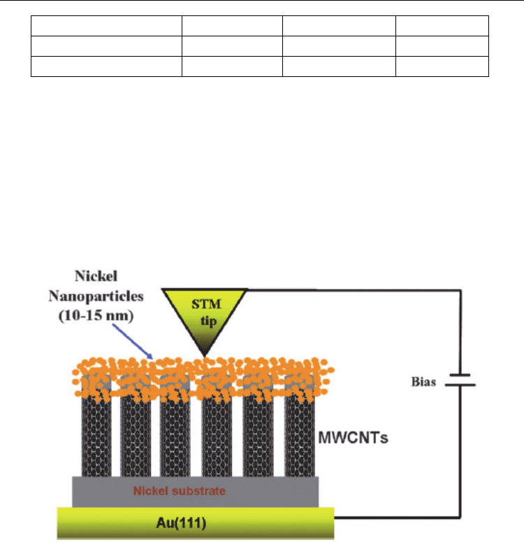
Figure 14 shows the simplest schematic configuration of the VCNT sample with a STM tip.
The nickel substrate act as a source that can generate a current of spin polarised electrons,
VCNTs act as a spacer that can transport spin polarised current and the nickel nanoparticle
deposit act as a sensor that can detect the spin polarised current. The STM tip acts as contact
to the top electrode and the Au to the bottom electrode. The magnetisation of the source
defines the spin direction of the charge carriers injected into the CNTs and the nickel coating
serves as a spin detector. Upon reversing the magnetisation direction of one of these
electrodes, the spin polarisation of the charge carriers arriving at the detector electrode will
be changed, giving rise to a change of the device resistivity, i.e., a magnetoresistance.
Fig. 14. Schematic diagram of spintronic devices.
Figure 15a shows the current-bias voltage (I-V
b
) curves of the sample at H = 0 T and H = 2 T
at 300 K. The Coulomb blockade region is observed between -1 V to 1 V and a stepwise
increment of the current (CS) is observed beyond the CB region. The (I-V
b
) curves exhibit
similar features at zero and applied magnetic field (parallel and antiparallel configuration).
The similarity in (I-V
b
) at zero and applied field is reported in literature. The magnified
portion of the green dotted square in the (I-V
b
) curves is shown in Figure 15b. A clear CS is
apparent in Figure 15b. The dI/dV vs. V
b
plot (see Figure 15c) exhibits clear peaks in a
periodic pattern beyond CB. The dI/dV vs. V
b
plot in the range (-1.9 to -1 V
b
) showing clear
periodic pattern is illustrated in the inset of Figure 15c. The bias voltage (V
b
) dependence of
MR derived from the normalised I-V
b
curves shown in Figure 15d. The oscillation of MR as a
function of bias voltage is observed.