Marulanda J.M. (ed.) Electronic Properties of Carbon Nanotubes
Подождите немного. Документ загружается.

22
Carbon Nanotube as VLSI Interconnect
Mayank Kumar Rai
1
and Sankar Sarkar
2
1
Department of Electronics and Communcation Engineering,
Thapar University, Patiala, Punjab
2
School of Electronics, Shobhit University, Meerut, U.P.
India
1. Introduction
A VLSI interconnect is a thin film of conducting material that provides electrical connection
between two or more nodes of the circuit/system formed in the silicon chip. Earlier the most
commonly used material was aluminum. The choice was based on its good conductivity
and adherence on silicon dioxide. Another useful property of aluminum is that it forms
good ohmic contact with silicon. As device density increased with technology scaling,
interconnect current density increased. A disadvantage with aluminum is that at high
current densities considerable electro migration takes place. Later it was realized that copper
a material of higher conductivity is several times more resistant to electro migration than
aluminum. In comparison with aluminum, copper can withstand about five times more
current density with equal reliability for IC-applications. Due to the advantages that it offers
copper became the preferred interconnect material, especially for submicron and deep
submicron high density, high performance chips. As the aggressive technology scaling
continues a new problem is surfacing. With decrease in cross-section copper interconnect
resistivity increases due to surface roughness and grain boundary scattering, causing
increase in propagation delay, power dissipation and electromigration [1-2]. To alleviate this
problem, for interconnects of future generation chips alternative solutions are under
consideration [1-14]. The most promising alternative for copper interconnects turns out to be
Carbon Nanotube (CNT).
The CNTs are grown in the form of seamless cylinders with the walls formed by one atomic
layer of graphite (graphene). The diameters of these cylinders are of the order of a
nanometer. These tubes are either metallic or semiconductor. For interconnect applications
the metallic ones are useful. There are two types of CNTs. Single walled CNT (SWCNT) and
Multiwall CNT (MWCNT). CNTs constituted by only one thin wall of graphene sheet are
SWCNTs. There are some CNTs which consist of a multiple of concentric SWCNT like
graphene tubes. These are termed MWCNT. The metallic CNTs are attractive interconnect
materials because of their high thermal and mechanical stability, thermal conductivity as
high as 5800W/mK, ability to carry current in excess of 10
14
A/m
2
current density even at
temperatures higher than 200°C and Fermi velocity comparable with that of a metal[15]. It is
very difficult to make a good contact with a CNT. The unavoidable contact imperfection
increases resistance. CNT resistances in the range 7 KΩ - 100 KΩ have been reported [16, 17].
Such a high resistance is a major disadvantage; if an isolated CNT is used as interconnect.

Electronic Properties of Carbon Nanotubes
476
The problem can be circumvented if for interconnect application CNT bundles are used
instead of isolated ones.
A CNT bundle consists of a large number of electrically parallel isolated CNTs. The result of
the parallel connection is considerable reduction of resistance between the ends of the
bundle. Therefore, a CNT bundle makes a better interconnect than the isolated counterparts.
The type of CNTs in a bundle is generally either SWCNT or MWCNT. In a bundle, some of
the constituent CNTs are metallic while others are semiconducting. The metallic CNTs
contributes to the formation of interconnect. MWCNTs are mostly metallic, whereas a large
fraction of CNTs in a SWCNT bundle are semiconducting. One type of MWCNT is a
DWCNT (double walled CNT). This form of CNT has been found to be a very useful for
application as interconnects.
2. CNT growth
The growth of on chip CNT bundle for commercial purposes is very challenging [18]. As
interconnect material SWCNT having higher conductivity is more preferable to the
relatively lower conductivity MWCNT. The cause of this conductivity difference between
the two types of CNTs is the much longer mean free path (about 1µm) of SWCNT as
compared to that of MWCNT (a few nm). So far it has been easier to grow MWCNT. The
process of CNT growth generally involves some catalyst particles (Fe, Ni, Co or their
compound with Mo). The catalysts assist growth process and controls tube diameter. To fill
via with CNT the catalyst particles are placed on the metal1 at the bottom of via. CNT is
then grown by chemical vapor deposition (CVD) at 450-800°C in presence of a carbon
containing gas [19].
Li et al. [20] proposed a bottom-up approach in which MWCNT via is grown on metal1. The
carbon fibers grow from Ni catalysts deposited at predefined locations. By means of PECVD
and an applied bias voltage the fibers are aligned perpendicular to the wafer surface. Finally
SiO
2
is deposited and the wafer is planarized. The planarization process also exposes the
CNT ends for contact with the metal 2 layer. This method yields high interconnect resistance
of the order of a few hundred kilo ohms. This is attributed to imperfections in the structure
of the MWCNTs thus grown. By this method high density growth could not be achieved. It
is suitable for growing single MWCNT fillings. A different approach is etching via down to
metal 1 layer and growing the CNTs in these vias [19, 21]. In [21] dry etching stops at a film
of the catalyst (Ni or Co). Arrays of MWCNTs are formed by hot-filament CVD (HF-CVD).
The resistance achieved by this method is about 30% of what the method of Li et al. [20]
results. Instead of HF-CVD, a pure CVD approach was adopted by Kreupl et al. [19]. This
method produced tubes of resistance of nearly 10 . In their approach, care is also taken to
ensure that via etching stops exactly on the catalyst layer so that highly reliable MWCNTs
are grown with density varying between 100 and 10000/μm
2
.
Earlier, arc discharge and laser ablation methods were used for growth of SWCNT [22, 23].
These processes involve evaporation of carbon from its solid form at temperatures as high as
3000°C or more. The high temperature requirement is not desirable. Another limitation of
these approaches is that the nanotubes formed are twisted around each other. This makes it
difficult to purify and arrange the CNTs for application purposes. More recently CVD with
methane as carbon source and iron oxide nano particles as catalyst has been used to grow
high quality SWCNT. The desired result is achieved in temperature range of 850-1000°C.
Carbon Nanotube as VLSI Interconnect
477
3.1 Problems of existing interconnect systems
With continuous reduction of feature size there has been a parallel increase in die size. The
result is more and more increase in length of some of the on chip interconnects as
technology scaling continues. Based on their length interconnects are categorized as local,
semi-global and global. A global interconnect is very long which is connected to several
nodes across the chip for example, clock lines, ground lines etc. The local ones connect
nearby nodes and are of shorter lengths. Interconnects of intermediate lengths are the semi-
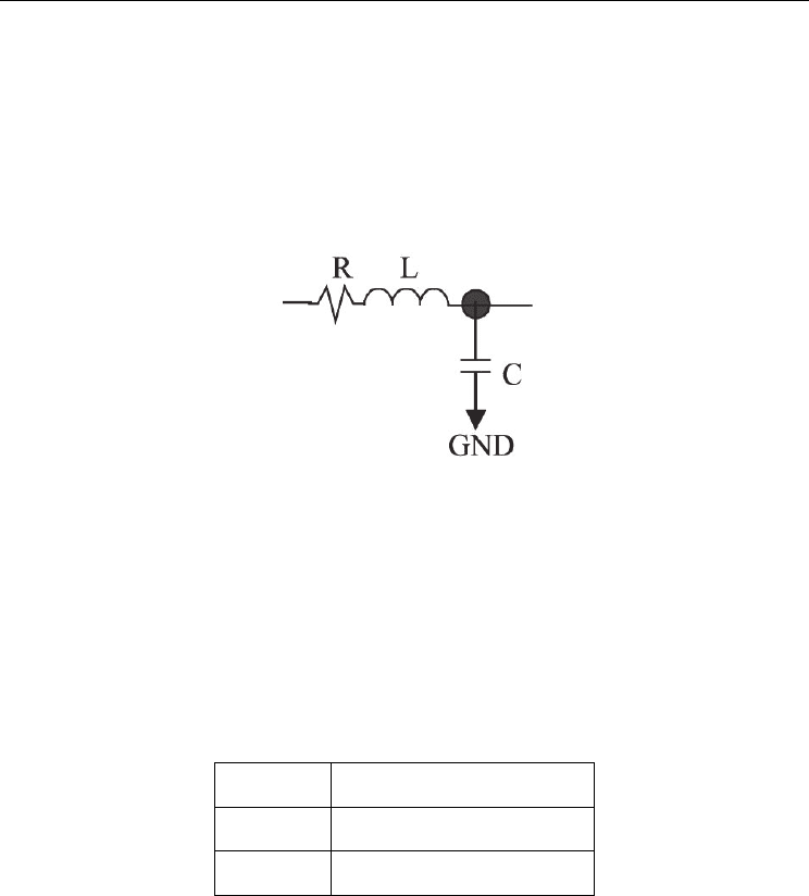
global ones. Interconnect is equivalent to an RLC circuit as shown in Fig. 3.1.
Fig. 3.1. RLC-equivalent of interconnect.
Any increase in interconnect length causes R, L and C to increase. This in turn results in an
increase in interconnect signal propagation delay. Thus as technology scaled signal delay
caused by interconnect became increasingly significant compared to delay caused by the
gate and thus affecting the circuit’s reliability. As per ITRS predictions [24], for nanometer
size gate lengths interconnect delay is mostly affected by resistive and capacitive parasitics.
For decreasing the resistive part of the RC delay, various alternatives to aluminum were
considered in early 1990s. As already discussed a metal of much better electrical resistivity
and electro migration than those of aluminum is copper. Table 3.1 compares the resistivities
of the two metals.
Metal Bulk resistivity (μΩ.cm)
Al 2.67
Cu 1.70
Table 3.1. Resistivities of aluminum and copper
Copper has a higher melting point (1,357 K) than aluminum (933 K). This provides more
thermal stability to copper. Because of these advantages copper is the most preferred on
chip interconnect material for the present day integrated circuits.
With advancement of VLSI technology, the number of on chip interconnects is on the rise.
To accommodate more interconnects the cross-sectional dimensions are reduced rapidly
resulting in dimensions of the order of mean free path of electrons in copper (~ 40 nm at
room temperature). As the dimension approaches electron mean free path grain boundary
and surface scattering are enhanced [25, 26]. Consequently, resistivity of interconnect is
increased. Another effect of dimension scaling is increase in current density. Thus as
Electronic Properties of Carbon Nanotubes
478
technology scales these effects on resistivity together with increase in interconnect resistance
with length enhances delay. Besides increase in delay, interconnect power dissipation
increases because of increased current density and increase in frequency of operation. The
increased heating due to the rise in power dissipation assists electro migration. As these
scaling dependent limitations of copper interconnect is going to be more and more severe
for the future generation of VLSI chips it is time to look for an alternative material. CNT
with all its advantage seems to be the right choice.
3.2 CNT interconnect
To analyze and understand the behavior of any interconnect (CNT or else) it is essential to
first develop its equivalent circuit (Fig.3.1). The development of an equivalent circuit is
complete only when various impedance parameters like resistance, capacitance and
inductance are fully defined by means of their analytical expressions. Such an equivalent
circuit is then used in analysis and simulation of interconnect performance.
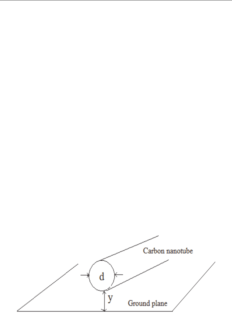
3.2.1 SWCNT interconnect
An isolated SWCNT on ground plane is shown in Fig.3.2. The separation between the
nanotube and the ground is y and the diameter of the SWCNT is d. Assuming it to be in
cylindrical form on the basis of Luttinger Liquid Theory, Burke [29] developed an electrical
equivalent of the structure as shown in Fig. 3.3. If a 1-D system has N conducting channels
in parallel then its resistance is h/Ne
2
T. Where h is Planks constant, e is electron charge and
T is electron transmission coefficient. Due to spin and sub lattice degeneracy of electrons
there are 4 parallel conducting channel in SWCNT (N=4). Thus assuming perfect contacts
(T=1), the resistance of an SWCNT is h/4e
2
. With the values of the physical constants
substituted the resistance assumes the fairly large value of 6.45 KΩ. In the equivalent circuit
(Fig.3.3) this resistance (R
f
) is equally divided between the contacts at the two ends of the
nanotube. That is,
R
f
= h/4e
2
(3.1)
Fig. 3.2. Carbon nanotube, of diameter ‘d’, distance ‘y’ below it.
Carbon Nanotube as VLSI Interconnect
479
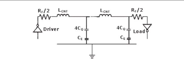
Fig. 3.3. Equivalent RLC circuit for an isolated SWCNT.
of length less than mean free path of electrons and assuming ideal contact. For lengths less
than one electron mean free path (L
0
), the tube resistance equals the fundamental resistance
given by (3.1). If the tube length (L) is larger than mean free path then enhancement of
scattering gives rise to an addition resistance. This resistance increases with increase in CNT
length and is
R
CNT
= (h/4e
2
)L/L
0
(3.2)
Making metal-CNT contact at the two ends of a tube is very complex. In most cases the
contacts are far from being perfect. The contact imperfection leads to very large resistance in
series with R
CNT
. CNT resistance of the order of 100 KΩ has been reported [31]. However,
resistances around the fundamental resistance are also observed in some cases. Thus the
resistance of a CNT has three components: the fundamental resistance R
f
, the scattering
resistance R
CNT
and the contact resistance at the two ends of the tube. CNT resistance is also
bias dependent. At higher bias where electric field is very high current saturates and CNT
does not show ohmic behavior. In the low bias regime on the other hand the CNTs show
perfect ohmic behavior and are compatible with VLSI interconnect applications.
CNT has two capacitances of different origins. One is electrostatic capacitance and the other
quantum capacitance. The electrostatic capacitance (C
E
) is due to charge stored by the CNT-
ground plane system (Fig.3.2) and is given by
C
E
= 2π
ઽ
/ln [ y/d] (3.3a)
This is per unit length of the nanotube.
The quantum capacitance (C
Q
) accounts for the quantum electrostatic energy stored in the
nanotube when it carries current. Considering this energy an effective capacitance (per unit
length) may be obtained which is expressed by
C
Q
= 2e
2
/(hv
f
) (3.3b)
Where v
f
is the Fermi velocity. Typically, C
Q
is 100aF/μm or so. As CNTs have four
conducting channels, total effective quantum capacitance resulting from four parallel
channel is 4C
Q
. When current flows both C
E
and 4C
Q
carry same charge. Thus the two
capacitances appear in series in the isolated SWCNT equivalent circuit (Fig.3.3).
For a SWCNT, there are two types of inductances termed magnetic inductance and kinetic
inductance. Magnetic inductance (L
M
) is due to the total magnetic energy resulting from the
current flowing in the wire. The kinetic inductance (L
k
) arises from kinetic energy stored in
Electronic Properties of Carbon Nanotubes
480
each conducting channel of the CNT. The four parallel conducting channels in a CNT results
in an effective kinetic inductance of L
k
/4. The expressions for L
M
and L
k
are
ln
2
y
L
M
d
(3.4)
L
K
= h/ {2e
2
(v
F
)} (3.5)
For d = 1nm and y = 1μm, L
M
(per unit length) and L
K
(per unit length) for a CNT is equal to
≈1.4pH/μm and 16nH/μm, respectively. Since, L
k
>>L
M
, inclusion of L
M
does not have
significant impact on the delay model for interconnects.
Fig.3.4 and 3.5, shows the equivalent Circuits of an SWCNT-bundle for L<L0 and L>L0 [29-
33]. Where L is bundle length. The resistances, inductances and capacitances of a bundle can
be obtained from the following expressions [29-33].
The CNT bundle resistance is given by (3.6) and (3.7), where H is thickness and w is the
width of CNT bundle interconnect, and n
CNT
is the total number of CNTs in the bundle.
2
0
4
CNT CNT
hL
RBundle n
L
e
(3.6)
1
1_ 1
2
33
22
CNT
wd Hd Hd
n
x
xx
(3.7)
If the number of rows in the bundle is even and
1
1_
2
33
22
W
CNT
nd
Hd Hd
n
x
xx
(3.8)
if number of rows is odd. The number of rows is given by (3.9) and x is the separation
between the centres of two neighbouring tubes. For parallel structure x=d.
H
n
=
1
3
2
Hd
x
(3.9)
The total effective capacitance of bundle of SWCNT is given by (3.10),Where
Bundle
E
C and
Bundle
Q
C are the total electrostatic capacitance and total quantum capacitance of bundle of
SWNT and are calculated by (3.11) and (3.12).
()
Bundle Bundle
EQ
Bundle Bundle
EQ
CC
C Bundle
CC
(3.10)
Carbon Nanotube as VLSI Interconnect
481
2
_2
222
23
25
ln ln ln
H
Bundle
ox ox ox
E
wd
n
x
C
ssws
ddd
(3.11)
2
2
Bundle
QCNT
f
e
Cn
hv
(3.12)
Where S is the separation between adjacent bundle. The inductance of CNT bundle is given
by the parallel combination of the inductances corresponding to each CNT forming the
bundle, which is
()
4
M
K
CNT
LL
LBundle
n
(3.13)
Where L
M
and L
K
are the magnetic and kinetic inductance of an isolated CNT.
The impedance parameters of a SWCNT bundle are calculated from (3.6) – (3.13) [33]. Table-
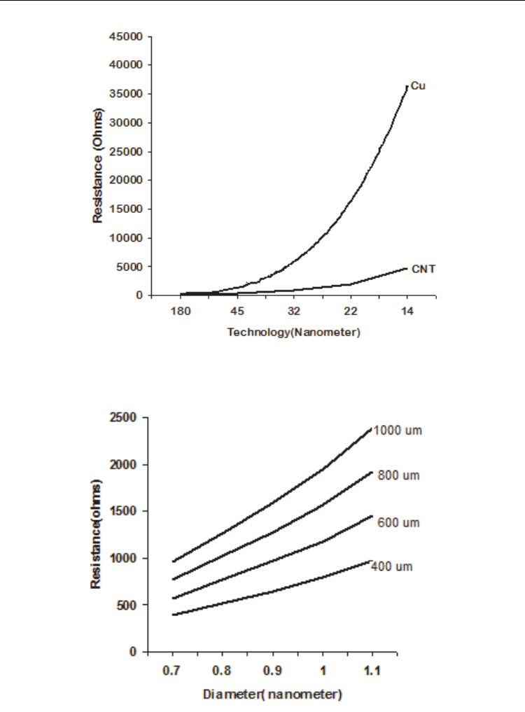
3.2, shows the data used for these calculations [33]. Fig. 3.6, shows how the resistance of
long (1mm) interconnects vary with technology scaling. It shows that in case of such long
interconnects the resistance of CNT interconnects is several times lower than that of copper
based interconnects in advanced technology nodes. The impedance parameters of CNT
interconnect are calculated from (3.1)-(3.13). For the sake of comparison the impedance
parameters of a copper interconnect are also determined. The Cu-interconnect impedance
parameters are determined by using expressions available in literature [34].
As may be seen from (3.6) through (3.8) the CNT resistance is a function of tube diameter d.
Fig. 3.7 illustrates the dependence of resistance on tube diameter. This is an example of the
dependence of SWCNT-interconnect resistance on tube diameter. It can be seen that a
bundle composed of tubes of larger diameters, when used as interconnect will have larger
line resistance.
The two CNT capacitances are calculated from (3.11) and (3.12). Fig.3.8 shows the variations of
SWCNT-interconnect capacitance with tube diameter. The decrease in capacitance with tube
diameter indicates the desirable effect of reducing interconnect delay. Increase in interconnect
resistance has the effect of increasing propagation delay. A comparison of Fig.3.7 and Fig. 3.8
therefore shows that two competing effects take place on delay as tube diameter is increased.
Much depends on which of the two is the dominating one. When the effect of resistance
dominates, delay rises as diameter increases. Otherwise the opposite effect takes place. If the
two effects balance each other, delay is independent of change in diameter.
Calculations using (3.4), (3.5) and (3.7) or (3.8) show that inductance in an SWCNT-bundle is
negligible in comparison with its resistance and capacitance. It is of the order of a few fH
(Fig. 3.9), which is much less compared to the several nano Henry of inductance that is
generally found in the copper interconnects. This shows that an SWCNT has negligible
inductive effect even in case of high-speed applications. Generally, interconnect delay
increases with increase in its equivalent resistance, inductance and capacitance [35]. As
inductive effect on CNT impedance is negligible, the dependence of resistance and
capacitance on tube diameter can provide insight into the variations of delays of the
SWCNT-interconnects with variation in tube diameter.
Electronic Properties of Carbon Nanotubes
482
The impedance parameters of interconnect is known to affect its delay and power
dissipation [36]. As the diameter of an isolated tube controls the impedance parameters of a
CNT bundle, it is of importance to study the effect of isolated tube diameter on delay and
power dissipation. The equivalent circuit shown in Fig.3.5 is used to SPICE-simulate signal
propagation down SWCNT-interconnect in 32nm and 22 nm technologies [37]. The clock
speed is 1.1MHz. Simulation is also carried out for copper-interconnects of same
technologies and clock speed. For simulation purpose copper interconnect is modelled by a
-equivalent circuit [38].
For both SWCNT and copper interconnects, 90% delay has been extracted from the SPICE
simulation results. Copper-interconnect propagation delay is used to normalize
corresponding SWCNT-interconnect propagation delays. From now onwards this
normalized SWCNT-interconnect delay will be referred to as ‘relative delay’. Similarly,
relative power dissipation in SWCNT-interconnect will mean normalization by copper
power dissipation. Fig.3.10 shows relative delay as function of isolated tube diameter. The
variations are simply reflections of the resultant of the effects of diameter variations on
resistance and capacitance taken together.
The relatively larger inductance of copper facilitates the lowering of the relative delay,
thereby placing SWCNT-bundle as a favourite candidate for future VLSI interconnects. The
gradual rise of relative delay in case of 22nm technology indicates dominance of CNT
resistance over its capacitance. For 32nm technology as diameter is increased the capacitance
dominates till a critical diameter is reached. Beyond this critical diameter resistance takes
over. Briefly, for good performance, the optimum tube diameter should be selected if
possible (32nm). Otherwise tube diameter should be restricted (22nm).
The diameter dependence of relative power dissipation in SWCNT interconnect is
illustrated in Fig. 3.11 at 32nm and 22nm technology nodes. As may be seen, in general
SWCNT-interconnect dissipate more power than its copper counterpart due to higher value
of tube capacitance. Furthermore, SWCNT interconnect power dissipation improves as
technology scales.
Power dissipation in SWCNT-interconnect can be lesser if the tubes are of larger diameter (Fig.
3.12). The diameter dependence of power results from the functional relationship between the
bundle impedance parameters and tube diameter. As SWCNT interconnects have negligible
inductance the decrease in CNT power dissipation with increase in tube diameter indicates
that the effect of capacitance dominates over the effect of resistance. Thus, reduction of
interconnect power dissipation by increasing tube diameter should be possible.
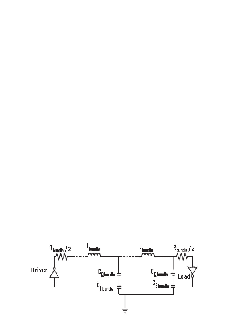
Fig. 3.4. Equivalent circuit diagram for SWCNT bundle interconnects (length L<L
0
where
L
bundle
=(L
M
+L
k
/4)/n
CNT
).
Carbon Nanotube as VLSI Interconnect
483
Technology 32nm 22nm
Vdd 0.9v 0.7v
Width(W) of local and semi global interconnect 32nm 22nm
A/R* 2 2
Thickness(H) of local and semi global interconnect 64nm 44nm
Separation(s) between adjacent bundle of local and semi
global
32nm 22nm
Width(W) of Global interconnect 48nm 32nm
A/R(Global) 3 3
Diameter of SWCNT 1nm 1nm
Thickness(H) of global interconnect 144nm 96nm
Separation(s) between adjacent bundle of global
interconnect
48nm 32nm
Oxide Thickness (t
OX
) 54.4nm 39.6nm
OX
(Relative)
2.25 2.05
*A/S (Aspect ratio) for local and Intermediate.
Table 3.2. Simulation parameters
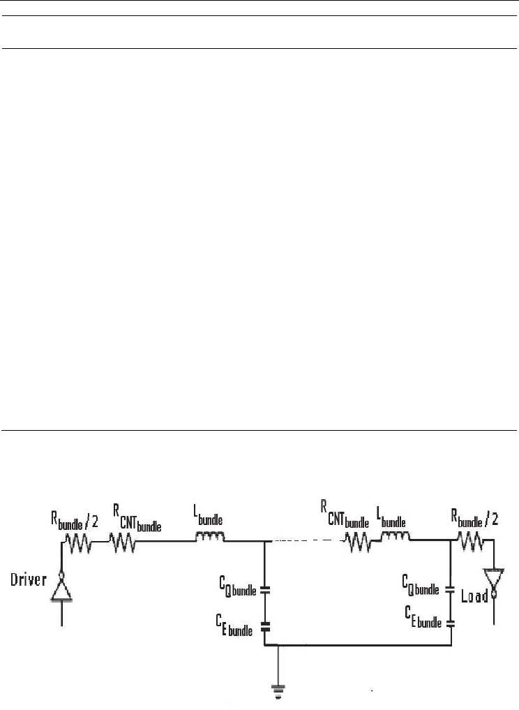
Fig. 3.5. Equivalent circuit diagram for SWCNT bundle interconnects ( length L>>L
0
where
L
bundle
=(L
M
)/n
CNT
).
Electronic Properties of Carbon Nanotubes
484
Fig. 3.6. Technology node dependence of resistances of long Cu [33]
Fig. 3.7. Variation of equivalent resistance with diameters at different interconnect lengths
for 22nm technology node [33].