Marulanda J.M. (ed.) Electronic Properties of Carbon Nanotubes
Подождите немного. Документ загружается.

23
Carbon Nanotube Based Magnetic Tunnel
Junctions (MTJs) for Spintronics Application
Elby Titus
1
, Manoj Kumar Singh
1
, Rahul Krishna
1
, Ricardo G. Dias
2
,
Antonio Ferreira
2
and Jose Gracio
1
1
Nanotechnology Research Division, Center for mechanical technology and automation,
Department of Mechanical Engineering, University of Aveiro,
2
Department of Physics and Institute for Nanostructures,
Nanomodelling and Nanofabrication (I3N), University of Aveiro
Portugal
1. Introduction
Spintronics devices exploiting the spin of the electron [1-10] are prepared to revolutionise
the electronics industry. The significance of this new generation device is faster memory and
lower power consumption at low electron density. The late 20
th
century has been considered
as an era of microelectronics. However, the avalanche growth of microelectronics is a major
threat to Moore’s law and spintronics may be a solution for it. From the first transistor to
the signally powerful microprocessor in our recent computers, most electronic devices have
employed circuits that express data as binary digits, or bits (1 and 0) represented by the
existence or absence of electric charge. Unlike microelectronics, spintronics exploits spin
(spin up ↑ and spin down ↓) of the electron to carry information between devices.
The discovery of Giant Magnetoresistance (GMR) by Nobel Prize winners Albert Fert and
Peter Grünberg had actually led to the birth of novel field spintronics [11]. Currently, most
of the existing spintronic devices [12] are based on metallic systems such as magnetic tunnel
junctions (MTJs) and single electron transistor [13]. On the other hand, a wealth of
intriguing spin phenomena has been observed in nanoscale materials [14]. This triggered an
extensive research effort on spin transport in nanoscale MTJs and other interesting
phenomena were realised. One of the most important phenomena is tunnel
magnetoresistance (TMR) of the MTJs. A MTJ is composed of two ferromagnetic conducting
layers separated by an ultra-thin insulating layer [15-20]. The TMR was first demonstrated
by M. Jullière [21]. Yakushiji et al. [22] experimentally demonstrated the influence of spin
conduction on TMR. The enhancement and oscillation of TMR in ferromagnetic multiple
junctions have been predicted by several authors [23-30]. However, there have been only a
few experiments on spin-dependent single electron tunnelling (SET) to date [31-36] due to
the difficulty in fabricating appropriate sample structures for spin-dependent SET.
The desire to build spintronic devices that show larger spin dependent phenomena has led
many researchers to combine single electron tunneling (SET) and spin dependent electron
tunneling (SDT). The charge quantization in low capacitance magnetic tunnel junctions

Electronic Properties of Carbon Nanotubes
496
(MTJs) can lead to SET phenomena represented by Coulomb blockade (CB) below a
threshold voltage and Coulomb staircase (CS) at higher voltages [37]. Carbon nanotubes
(CNTs) can actually be thought of as a spacer in MTJ devices due to its one dimensional
nano structure with ballistic conduction. It can control current transport by quantum
mechanical spin degree of freedom. The remarkable spin dependent phenomena are
expected in these devices due to the interplay between SET and spin dependent electron
tunneling (SDT). In this chapter, we explore the state of the art MTJ devices with special
emphasis to CNT. Novel phenomena, TMR and SET in spintronics devices are highlighted.
2. Spintronic devices
The working principle of a spintronic device follows the steps (i) information is stored into
spins as an orientation (i.e. up or down), (ii) spin information is carried by mobile electrons
along a path or wire and (iii) the information is then read at a final point. Figure 1 shows the
schematic representation of a spintronic device. The spin orientation of conduction electrons
will exist for several nanoseconds making them useful in electronic circuit and chip design.
The most basic method of creating a spin-polarized current is to transport current through a
ferromagnetic material and to transmit the electron spin carrying the information to the
receiver point. Spin current is therefore an important tool to detect spin in spintronic
devices. The important avenues for the development of spintronics devices are: (i)
fabrication of nanoscale nanostructures including novel magnetic materials, thin films,
hybrid structures, and functional materials, (ii) research on spin effect (spin injection, and
spin transport and detection), (iii) demonstration of spintronic devices including giant
magnetoresistance (GMR) and tunnel magnetoresistance (TMR) devices in magnetic tunnel
junctions (MTJs) and (iv) study of SET in MTJs.
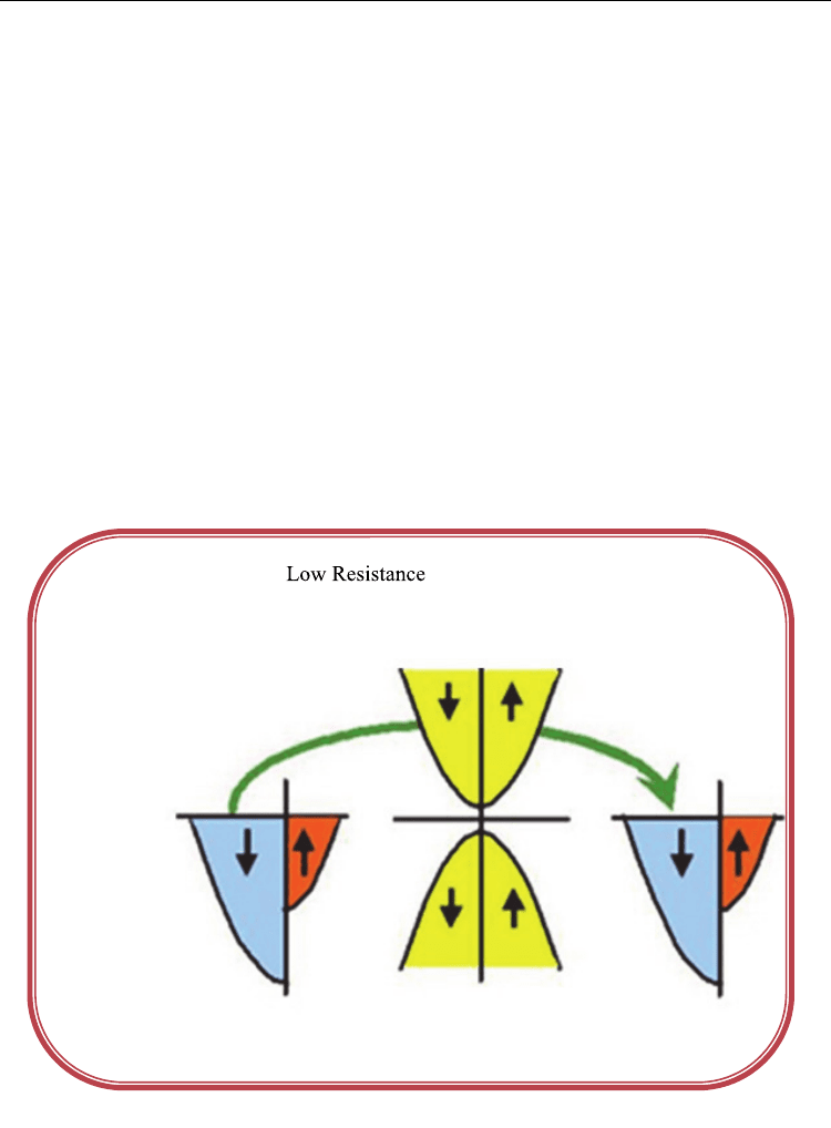
3. Magnetic Tunnel Junctions
A magnetic tunnel junction (MTJ) can be considered as a spintronic device since it is
composed of two ferromagnetic materials, such as nickel, cobalt or iron, separated by an
ultrathin layer of insulator with a thickness of the order of nanometre (10
-9
m). It exhibits two
resistances, low (R
p
) or high (R
ap
) depending on the relative direction of ferromagnet
magnetizations, parallel (P) or antiparallel (AP), respectively. The insulating layer is so thin
that electrons can tunnel through the barrier if a bias voltage is applied between the two
metal electrodes. The schematic of a magnetic tunnel junction (MTJ) is illustrated in Figure
2. In MTJs the tunneling current depends on the relative orientation of magnetizations of the
two ferromagnetic layers, which can be changed by an applied magnetic field. This
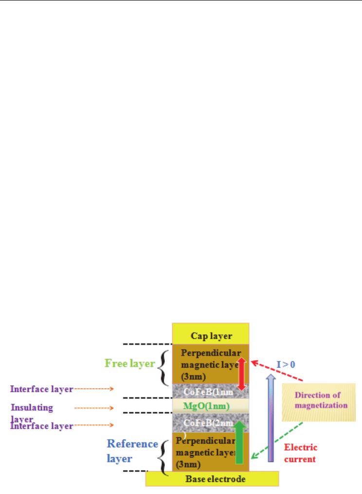
phenomenon is called tunnel magnetoresistance (TMR). An important factor in TMR is the
interaction between the electron spin (S) and angular momentum (L) that is, spin orbit
coupling (SOC). An example of SOC is splitting of hydrogen spectrum [38-40]. The SOC
deforms the electron shell as the direction of the magnetization rotates. This deformation
also changes the amount of scattering undergone by the conduction electrons when
traversing the lattice. There will be minimum resistance if the magnetizations are in parallel
orientation and it will go to maximum with opposite orientations (Figure 3). Therefore, such
kind of junction can be easily switched between two states of electrical resistance, one with
low and one with very high resistance.
Carbon Nanotube Based Magnetic Tunnel Junctions (MTJs) for Spintronics Application
497
Fig. 1. A Schematic representation of spintronic device.
Fig. 2. A Schematic magnetic tunnel junction (MTJ).
Electronic Properties of Carbon Nanotubes
498
3.1 Fabrication of MTJs
The fabrication of MTJs
with high TMR ratios is crucial in developing spintronic devices.
With the advance of nanotechnology, there are various methods to deposit MTJs, such as
molecular beam epitaxy (MBE), magnetron sputtering, electron beam evaporation and
chemical vapour deposition (CVD), and so on. In detail, the MTJ’s main components are
ferromagnetic (FM) layer and insulator layer. The FM layers can be fabricated by sputter
deposition (magnetron sputtering and ion beam deposition). The fabrication issue is the
magnetic alignment and thickness (deposition rates should be in the Angstrom-per-second
range). The best way of fabricating insulating layer is still under research. Some of the
proven materials are Al
2
O
3
tunnel barriers made by depositing a metallic aluminium layer
in the range of 5-15 Å thickness. In addition, ion beam oxidation, glow discharge, plasma,
atomic-oxygen exposure and ultraviolet-stimulated oxygen exposure are also alternate ways
of insulator deposition. Since the first report on TMR by Julliere [21], many studies have
been performed to explore this property, especially on Al
2
O
3
insulating layers. The necessity
of controlling the magnetic properties of the magnetic layers introduces special
requirements on the deposition process. The maintaining of inherent magnetic anisotropy is
crucial in the deposition process. This can be set by applying magnetic field during
deposition. The thickness & uniformity of the material, the coercivity, magnetorestriction, all
are important in controlling the magnetic anisotropy.
Fig. 3. Resistance goes from minimum to maximum with change in magnetization
orientation from parallel to anti-parallel.
Carbon Nanotube Based Magnetic Tunnel Junctions (MTJs) for Spintronics Application
499
There are some theoretical predictions stating the MTJs with maximum TMR ratios could be
fabricated by the epitaxial growth of ferromagnetic-non ferromagnetic-ferromagnetic
nanoscale sandwich structure, Fe/MgO/Fe and Fe/MgO/FeCo [41, 42]. The high ratios
resulted from the effective coupling of the majority spin band of Fe/FeCo into MgO and
MgO into Fe/FeCo. TMR ratios up to 180% and 220% were achieved in these structures [43,
44]. The literature also says MTJs can be fabricated using half-metallic ferromagnets [45] and
can generate 100% spin polarization at Fermi level (EF) due to the energy gap for one spin
direction. The maximum spin polarization up to 100% is highly desirable in spintronic
devices for the efficient spin injection from ferromagnetic electrodes into the non-
ferromagnetic spacer and for the development of current induced magnetization switching
in MTJs. Other MTJs with half-metallic ferromagnets which have shown higher TMR at
room temperature are cobalt based alloy thin films including Co
2
Cr
1-x
Fe
x
Al, Co
2
MnSi or Co-
Mn-Al. In addition to MgO tunnel barrier, aluminium oxide also been used as tunnel barrier
with ferromagnetic electrodes Co
2
Cr
0.6
Fe
0.4
Al and Co
2
MnSi. The advantage of these alloys
is the high Curie temperature above room temperature. N. Tezuka et al have developed a
MTJ of Co
2
FeAl
0.5
Si
0.5
electrodes and a MgO barrier fabricated by MBE and observed that
their device had a TMR ratio of 386% at approximately 300K and 832% at 9K [46].
Nowadays, magnetic data storage technologies prefer perpendicular magnetic anisotropy
(PMA) compared to the conventional devices that exploit the magnetization of the layers
within the film plane. Figure 4 shows the cell structure with perpendicular magnetic
anisotropy. An alloy of cobalt-iron is employed in the magnetic layer, with magnesium
oxide in the insulating layer and cobalt-iron-boron in the interface layers. The structure
developed by Toshiba is used for recording media. PMA has also been observed in several
ferromagnetic materials including multilayers such as Co-Pt, Co-Pd, Co-Ni, CoFe-Pt, and
CoFe-Pd, Co-Cr-Pt, alloys such as CoPt, FePt, and CoCr, and rare-earth transition metal
alloys [47-50]. However, an ideal system with high thermal stability at nanoscale dimension,
low current induced magnetization and high TMR was not successful. In view of this, S.
Fig. 4. Magnetoresistive random access memory (MRAM) with giga bits capacity developed
by Toshiba.
Electronic Properties of Carbon Nanotubes
500
Ikeda et al [51] employed interfacial PMA between the ferromagnetic electrodes and the
tunnel barrier of the MTJ by using the material combination of CoFeB–MgO. The MTJs
consisting of Ta/CoFeB/MgO/CoFeB/Ta showed a high TMR ratio, over 120%, high
thermal stability at dimension as low as 40 nm diameter and a low switching current of 49
μA.
3.2 TMR in MTJs
To continue the discussion, TMR is a magnetoresistive effect that occurs in component
consisting of two ferromagnets separated by a thin insulator (MTJ). The interest towards
TMR is driven by the fact that MTJs with spin dependent tunneling (SDT) are expected to
provide technical promises that will allow the realization of nanoscale devices in more
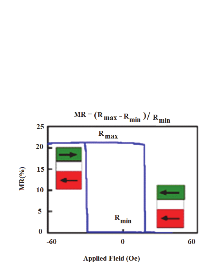
advanced spintronic applications. T. Moodera et al [52] fabricated the first reproducible
TMR up to 24% (Figure 5) at room temperature on CoFe/Al
2
O
3
/Co or NiFe junction. Today,
reproducible TMR value up to 50% can be obtained with three dimensional ferromagnets
making them useful for industrial application [ 53].
Fig. 5. Ratio of tunnel magnetoresistance (TMR) shown in CoFe/ Al
2
O/ Co junction., J. S.
Moodera, L. R. Kinder, T. M. Wong, and R. Meservey, Phys. Rev. Lett. 74, 3273 (1995) ©
American Physical Society
3.2.1 Theory of TMR
The TMR effect in MTJs can be derived using Julliere’s model [21, 51-53]. According to this
model the magnetoresistance,

Carbon Nanotube Based Magnetic Tunnel Junctions (MTJs) for Spintronics Application
501
TMR = (R
AP
-R
P
)/R
P
= 2P
2
/ (1-P
2
) (1)
where R
P
and R
AP
are the resistance in parallel and antiparallel magnetic configuration,
respectively and P is the spin polarization. The Differential TMR can be re-written as
TMR =
11
1
//
/
AP P
AP
dI dV dI dV
dI dV
(2)
According to Wiesendanger [54] the derivative of an I-V curve (the differential conductivity
is expressed as
2
2
12
2
FF
dI e
tD E DE eV
dV
(3)
where
2
t is the tunnel probability, D
1
and D
2
are the DOS of the two electrodes, E
F
is the
Fermi energy, and V is the bias voltage applied to the electrode at low temperature.
The injection of spin currents from a ferromagnetic manganite, La
0.7
Sr
0.3
MnO
3,
into a single
CNT (non-ferromagnetic) and the transformation of spin information into large electrical
signal have been demonstrated by L. E. Hueso et al [55]. The TMR calculated in their system
is 61%. R. S. Liu et al. [56]
observed TMR (10%) due to the interplay of SDT and CB in a
Ni/NiO/Co/NiO/Ni double junction of a submicron scale. Interestingly, both the systems
are MTJ which is similar to our system. H.B Peng et al. [57] also studied I-V characteristics
on patterned growth of SWCNT arrays from vapour-deposited Fe catalyst. Similar I-V
features were observed in Nickel-CNT-Nickel MTJ system fabricated by the current authors
[58]. Undoubtedly, Coulomb blockade (CB) effect, the principle of single electron tunnelling
(SET), is responsible for the enhanced TMR in nanoscale MTJs. The SET phenomena and the
associated MR occur only if the transport of electrons from one electrode to another is
inhibited due to the extremely high electrostatic energy e
2
/2C (e = charge of electron and C is
the capacitance) of a single electron compared to the thermal energy k
B
T. When the bias
voltage increases and exceeds the threshold V
th
= e/2C, the current starts to increase. If the
resistance of two junctions are similar (R1≈ R2), the current increases smoothly with bias
voltage. T. Niizeki et al [59] could reduce the junction area to 10nm and observed enhanced
TMR due to the coulomb blockade (CB) effect.
Motivated by the possibility of spintronics, the current authors have attempted a novel MTJ
system using vertically aligned CNTs [58, 60]. The TMR along with Coulomb blockade and
Coulomb staircase was observed in our system. Our device is formed of a vertical array of
carbon nanotubes bridged between the nickel electrodes. The higher value of CB spacing (~
2 V) in our system compared to the reported value (0.8V)
is expected due to the bulk effect
of CNT arrays. It also confirms that there is no short connection in the sample. From the I-V
analysis of our system it appears that TMR is originating from the spin polarisation of the
electrodes, i.e the difference between the density of states (DOS) of the up-and down-spin
sub-bands in the two electrodes. More details of CNT- MTJs are given section 2.2.
3.2.2 Characterization
It is well known that the TMR is highly sensitive to the structural and chemical nature of the
material. The characterization techniques such as electrical conductivity, magnetoresistance

Electronic Properties of Carbon Nanotubes
502
and tunneling microscopy can give detailed information on MTJs properties. The
knowledge on magnetic property of the ferromagnetic electrodes is crucial in development
of MTJ devices. The superconducting quantum interference device (SQUID) is the most
sensitive magnetic field equipment to measure the magnetic property. It has enough
sensitivity to measure measure the magnetic fields in nanoscale ferromagnets. The
magnetization of the material can also be measured by vibrating-sample magnetometer
(VSM) technique. VSM is based on Faraday’s law which implies that an emf will be
generated in a coil when flux changes in the coil. TMR also can be measured using the four
probe method by sweeping the magnetic field. Scanning tunneling spectroscopy
(STS)/scanning tunneling microscopy (STM) is another technique which can give precise
TMR measurements. The details of all these measurements are given in section 5.
3.3 Application of MTJs
With wider knowledge on how to manipulate spins [61], we can build more state of the art
spintronic devices with extraordinary properties. Extended research into application
possibilities of any spintronic effects is therefore crucial to realise more advanced spintronic
devices. These devices made huge impact on computer technology by enabling higher
storage of information in hard drives and faster reading of data in random access memories.
The first successful application of MTJ was demonstrated in computer read head technology
with Al
2
O
3
barrier and MgO barrier MTJ. The magnetic recording density in hard disk drive
increased (300-600 Gbit/Inch
2
) considerably in these devices [62-65]. Another application of
MTJ is to develop magnetic random access memory (MRAM) devices. It has been claimed
that MRAM can exceed the speed of SRAM (static RAM), density of DRAM (Dynamic RAM)
and non-volatility of flash memory. In addition, the nano-dimension device has low power
consumption and less heating. MRAM is an upgrade version of SRAM and DRAM where
data is stored using spin instead of electrical charges. It overcomes one of the disadvantages
of the conventional RAM, the loss of information by power failure. Leading companies like
IBM, Motorola, and Honeywell started the MRAM research in 1995 and they were
supported by United States Defense Advanced Research Projects Agency (DARPA). Figure 6
shows the images of MRAM used by leading companies like Thoshiba, IBM and Motorola.
4. Spin current in MTJs
In the view of rapid progress in the fabrication of nanoscale MTJs, spin is a subject of great
interest. Spin is a purely quantum mechanical quantity which provides an extra degree of
freedom for the electron to interact with a magnetic field. In 1922, Stern and Gerlach
demonstrated the most direct experimental evidence of the existence and of the quantized
nature of the electron spin. The first experimental evidence of spin dependent tunneling was
reported by Jullerie [21] in 1975. Later, Berger proposed the idea that spin polarized current
act on local magnetization of ferromagnets and leads to giant magnetoresistance [66]. The
important property of spin is its weak interaction with the environment and with other
spins, resulting in a long coherence or relaxation time, which is a very important parameter
in the field of spin-transport and quantum computing. For the successful incorporation of
spins into the currently existing electronics, one has to resolve issues such as efficient spin
injection, spin transport, control and manipulation of spins and finally detection of spin
polarized current.
Carbon Nanotube Based Magnetic Tunnel Junctions (MTJs) for Spintronics Application
503
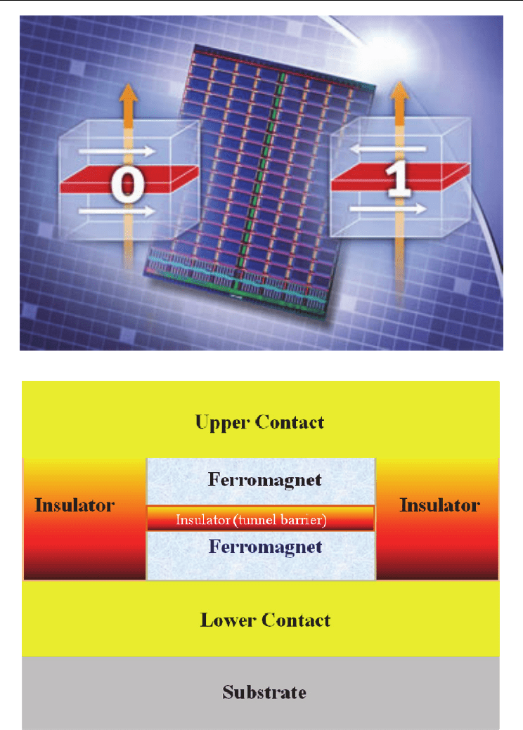
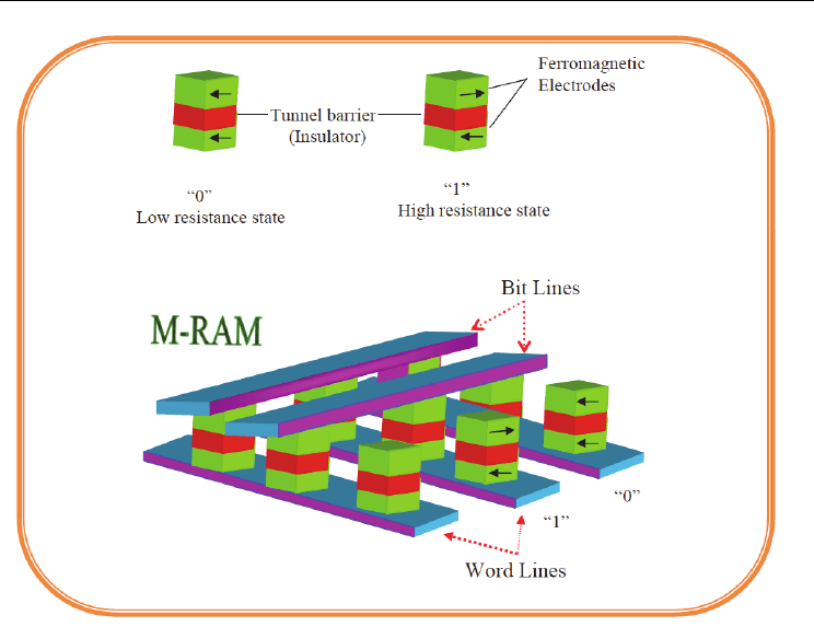
Fig. 6. MRAM memory cells composed of a magnetic tunnel junction (MTJ). States "0" and
"1" in the cells correspond to the parallel and antiparallel alignments of the electrode
magnetic moments.
Spintronics without magnetism is an attractive pathway for designing semiconductor
spintronic devices since spin orbit coupling (SOC) enables that the spin is generated and
manipulated merely by electric field. By the application of electric field, the electrons move
in the lattice generating a magnetic field which acts up on the spin. The spin orbit
interaction on mobile electrons was proved theoretically many decades ago. However, the
practical harnessing of this concept is still at an early stage
4.1 Spin transport
The influence of spin transfer in MTJs can be observed by measuring resistive loops as a
measure of external applied field and applied voltage. By sweeping the magnetic and
electrical field, one can observe sharp drop in resistance which is attributed to the switching
from parallel to antiparallel and vice versa. The drop of resistance is associated with the
TMR. One of the factors that affect drop of resistance and TMR is density of states (DOS) at
the interface [67-71].
4.2 Spin polarization
In addition to the spin transport, spin injection and spin polarization also an important
factors in governing TMR. The spin polarization is a result of a subtle cancellation between

Electronic Properties of Carbon Nanotubes
504
two spin channels and is greatly influenced by the atomic, electronic and magnetic
structures of the system. While the fundamentals of electron tunnelling are well understood,
the quantitative theoretical description is lacking in real systems due to limitations in
fabrication. Sophisticated and stable nanofabrication method will solve the problem of
interface in MTJs. However, to build up on experimental findings, it is also essential to
develop an accurate model of the spin polarization and transport of spin current through
the ferromagnetic/nonferromagnetic interface and finally into vacuum which is highly
sensitive to the chemical and material details of the device. In this context, Density
functional theories [72] of MTJ system that can produce spin polarization effects in the
Fermi Energy (FE) are important. Density functional theory (DFT) is a widely used
method for modelling charge/spin carrier transport semiconductors. There is plenty of
literature on DFT based calculations in studying SDT in MTJs [73-75]. The key
components in the modelling are schottky barrier (φ
b
) and the applied voltage V
A
against
current density. Ab initio simulation of magnetic tunnel junctions has been demonstrated
by Derek Waldron et al [76]. The effect of schottky barrier profile on spin dependent
tunnelling in a ferromagnet-insulator-semiconductor system is reported in N.L.Chung et
al’s work [77].
4.3 Theoretical modelling
Landauer [78] formula is really useful in order to compute spintronic devices. For the
simplicity of modelling, the system can be assumed as one-dimensional, composed by a
quantum wire with length L and two ferromagnetic reservoirs with electrochemical
potential μL and μR which are given by
μL
↑↓
= E
F
+(-)∆µ,
μR
↑↓
= E
F
+(-)∆µ + V
A
,
∆ µ = (µ↑-µ↓)/2 being half of the spin splitting energy. The effect of the Schottky barrier is
important on the SDT and therefore negligible spin relaxation in the tunnel barrier should
be considered.
If f is a function in the k space, the sum of f over k is given by
(4)
Let us assume that the transport in the channel is ballistic and the electrons entering the
reservoir is in equilibrium. The positive current, carried by the k> 0 state in i subband is
then given by
(5)
where υi is the velocity and f is the Fermi-Dirac distribution function.
Using
∑
→2
(6)
eqn 6 can be rewritten as