Marulanda J.M. (ed.) Electronic Properties of Carbon Nanotubes
Подождите немного. Документ загружается.

Carbon Nanotube as VLSI Interconnect
485
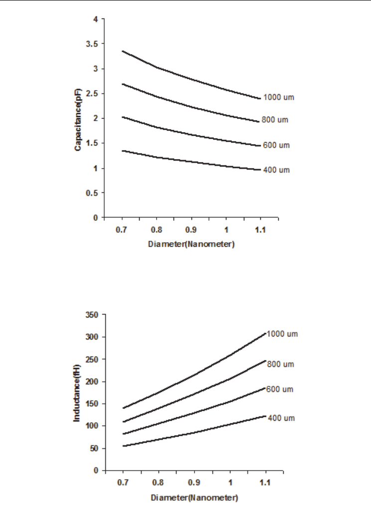
Fig. 3.8. Variation of capacitance with tube diameter at different interconnect lengths for
22nm technology node [33].
Fig. 3.9. Variation of inductance with tube diameter at different interconnect lengths for
22nm technology node [33].
Electronic Properties of Carbon Nanotubes
486
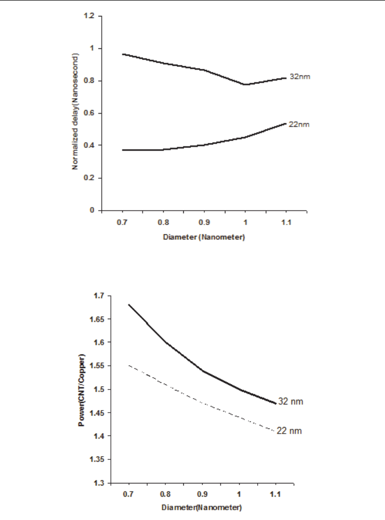
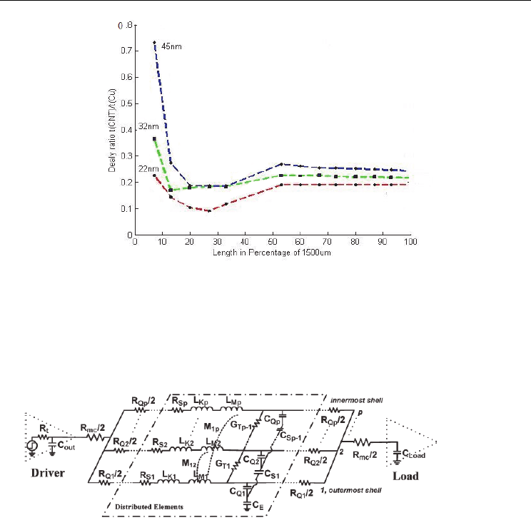
Fig. 3.10. Tube diameter dependence of normalized SWCNT bundle interconnect
propagation delay in two different technology nodes with Interconnect length=1mm [33].
Fig. 3.11. Relative power dissipations as function of tube diameter with length 1mm as
parameter for 32nm and 22nm technology node [33].
Carbon Nanotube as VLSI Interconnect
487
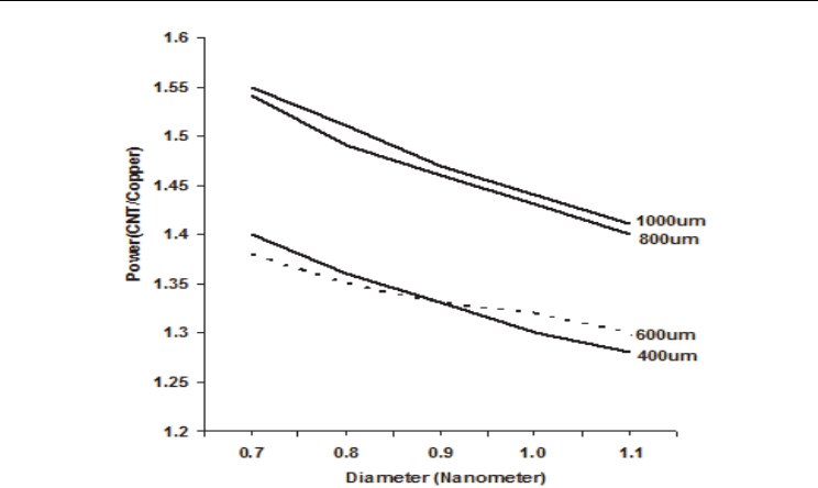
Fig. 3.12. Relative power dissipations as function of tube diameter with length as parameter
for 22nm technology node [33].
Srivastava et al.[31], Li et al[39] and Massoud et al[40], analyzed the performance of the
CNT interconnects of all three categories of interconnect length.
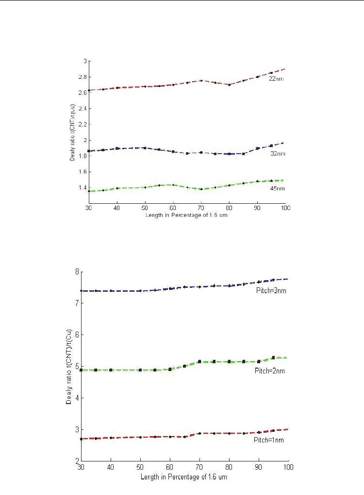
A comparison of propagation delays of CNT bundle interconnect and Copper interconnect
[31, 41] is shown in Fig.3.13. In this figure 38% length corresponds to 0.6µm and 100%
corresponds to 1.6µm. The lengths of the local interconnect are of this order and are
comparable to mean free path of electrons in CNT. Fig.3.13 shows that the delay of CNT
bundle is larger than that of copper interconnect. The difference between the two increases
as technology advances. The analyses of simulation results [31,39, 40] also indicate that non-
zero metal-nanotube contact resistance degrades CNT-interconnect performance, however,
its impact is negligible. Furthermore, in case of sparse bundle the performances of a CNT
interconnect is better [39]. The dependence of propagation delay ratio on interconnect
length was also studied [31,41].
For the local interconnects, the influence of pitch on delay of CNT bundle is quite significant
(Fig. 3.14.). It can be seen that the delay ratio of CNT bundle to copper interconnect is
increased when the pitch increases. This, however, does not agree with what is reported in
[40]. Fig.3.13 and Fig.3.14 also show that the delay ratio change very slowly as interconnect
length is increased. This may be attributed to ballistic transport in CNT because of its low
resistance.
Li et al. [39], analyzed propagation delay ratios of CNT and copper semi- global and global
level interconnects. Fig.3.15, illustrates a comparison between CNT and Copper interconnect
delays at these levels. It can be seen that the propagation delay-ratio of CNT and copper
interconnect is very high at the local level, but undergoes a steep decrease as we move to the
semi- global level where it first decreases to a minimum value and then increases by a slight
amount. Finally it becomes constant at lengths of global level. From Fig.3.15, it is clear that a
CNT interconnect gives best performance at the semi-global level because the propagation
Electronic Properties of Carbon Nanotubes
488
delay ratio of CNT to Copper interconnect attain low values at lengths in the range of 200m
- 650m. It can be observed that in the semi global and global regimes the performance of
CNT interconnect is better than that of copper interconnects.
Fig. 3.13. Comparison of propagation delay between CNT bundle and copper interconnects
[41].
Fig. 3.14. Propagation delay ratio of densely packed CNT bundle to copper interconnects at
different pitches [41].
Carbon Nanotube as VLSI Interconnect
489
Fig. 3.15. Propagation delay ratio of densely packed CNT bundle to Cu interconnect [41].
3.2.2 MWCNT interconnect
The complex structure formed by a large number of concentric tubes makes analysis and
design of MWCNT interconnect to be difficult. For analytical purpose Hong et al.[42]
proposed an equivalent circuit model as shown in Fig. 3.16.
Fig. 3.16. Equivalent circuit model of a MWCNT with p shells [42]
This figure shows the equivalent circuit model of a MWCNT with p shells. R
mc
/2 are contact
resistances at the two ends of the MWCNT. Lumped quantum resistance per shell is R
Q
. R
S
is the scattering resistance. L
K
is kinetic inductance. Magnetic inductance is L
M
. The mutual
inductance is M. Quantum capacitance is C
Q
and C
E
is the electrostatic capacitance between
the outermost shell and ground. Other shells do not have this capacitance. C
S
is shell
to shell capacitance. G
T
is tunneling conductance that has p – 1 components for the
MWCNT. R
t
and C
out
are respectively resistance and output capacitance of the driver. These
impedance parameters can be calculated from those available in literature [42].
SPICE simulation using the equivalent circuit (Fig.3.16) shows that as in the case of SWCNT
the resistivity of MWCNT bundle is also length dependent. For longer length (> 10 µm),
MWCNT resistivity is much lower than that of copper interconnect and is comparable
SWCNT interconnect. The simulation results show that for global interconnects delay in
MWCNT interconnect is less than delay in copper interconnect. The delay improvement

Electronic Properties of Carbon Nanotubes
490
further enhances with increase in interconnect length. However, increase in interconnect
width deteriorates MWCNT delay. A better performance can be achieved if MWCNTs of
larger diameters form the MWCNT bundle interconnect.
Hong et al. also studied MWCNT delay at semi global and local levels of length. They
observed that in range of semi global length MWCNT interconnects are significantly faster
than their copper counterparts. Furthermore, technology scaling improves delay
performance. The local interconnects have smallest cross section which results in substantial
resistivity. As a result line delay is more in the local interconnects. Over this range of
interconnect length the copper interconnect yield better performance.
3.2.3 Comparison of SWCNT with MWCNT interconnects
It is amply clear from the foregoing discussions that at highly scaled technologies for global
and semi global interconnects both SWCNT and MWCNT can be appropriate replacements
for copper. Between the two forms of CNTs SWCNT should have been the choice because of
its lower resistivity resulting from longer mean free path. In reality this advantage cannot be
taken as random chirality (direction in which graphene sheet is rolled up) leads to a large
number of semiconducting tubes in a bundle. These semiconducting tubes do not
participate in the conduction process. Growing a totally metallic SWCNT bundle is
challenging job. Relatively simpler growth process and the highly metallic nature of the
MWCNT interconnect makes it a better option at present. Its disadvantage is the short mean
free path.
Simulation results [41-42] show that both SWCNT and MWCNT interconnect performs
better than copper interconnect at global and semi-global levels. A highly metallic SWCNT
out performs the MWCNT, especially at highly scaled technology. However, in reality
existence of a population of semiconducting constituents in SWCNT bundle causes
MWCNT to perform better. In local level MWCNT marginally outperform SWCNT.
4. Cross talk between CNT interconnects
Because of capacitive and inductive coupling between adjacent interconnects signal
propagating down one (aggressor) affects signal propagating down the other (victim). This
is commonly referred to as crosstalk. Crosstalk in copper and aluminum interconnects are
extensively studied [43-46]. It is now well established that in such interconnects crosstalk
induce signal delay, overshoot, undershoot and glitches in the victim. These aberrations
travel down interconnect and cause faulty operation of the receiving device. However, very
little work has been done in the area of crosstalk in CNT interconnect.
Rossi et al. [47] are the first to study crosstalk in CNT interconnect. They analyzed crosstalk
in CNT interconnect implemented bus architectures. Both SWCNT and MWCNT
interconnects were considered. It was shown that delay and voltage noise margins in
MWCNT busses are much better than SWCNT busses. The crosstalk delay is also lower in
the SWCNT busses. In these busses cross delay can be improved by optimizing the spacing
between the interacting interconnects. Furthermore, crosstalk induced logic error in the
output device can be considerably large in case of MWCNT where as no such problem
occurs in SWCNT architecture. Rossi et al. also proposed a crosstalk aware CNT bus
architecture. This architecture is formed by double walled carbon nanotubes (DWCNT) in
parallel. It is shown to be significantly less susceptible to cross talk produced delay and
noise voltage peaks.

Carbon Nanotube as VLSI Interconnect
491
Pu et al. [48] developed analyzed crosstalk effects in SWCNT and DWCNT interconnects.
Their analysis included coupling inductance along with coupling capacitance. The analytical
crosstalk models thus developed capture crosstalk delay, glitches etc. with good accuracy.
Crosstalk induced delay in SWCNT and DWCNT bundle interconnects were compared with
that of copper interconnect. It is observed that for semi-global and global interconnects CNT
especially DWCNT results in much reduced crosstalk induced signal delay. For suppression
of crosstalk induced glitch copper interconnect is better.
The crosstalk induced voltage peaks produce stress in oxide layers underlying the victim
interconnect. With technology scaling oxide thickness has drastically reduced. As a
consequence of oxide thinning a small crosstalk produced overshoot or undershoots causes
a prohibitively large electric field to generate across the oxide. With time such electric field
weakens the oxide layer and possibility of its damage increases. The possibilities of oxide
damage due to crosstalk overshoot and undershoot was studied by Das and Rahaman [49].
They observed that with scaling ratio of overshoot/undershoot voltages to power supply
voltage does not vary with scaling in all types of interconnects. However, in case of copper
interconnects overshoot and undershoot increases as interconnect length is increased. In
case of the CNT based interconnects on the other hand, neither scaling nor increase in length
affect crosstalk induced voltage overshoot and undershoot.
5. Conclusion
An over view of the exploratory research on CNT as possible VLSI interconnect is
presented. The problem of continuing with copper interconnects in highly scaled
technologies of future are briefly discussed. The works carried out in finding an alternative
solution indicates that the CNT based interconnects have the potential to replace copper in
future. The SWCNT bundle is most desirable form of CNT based interconnect provided all
constituent CNTs of the bundle are metallic. The SWCNT has been studied extensively and
it is found that isolated tube diameter plays an important role in determining delay and
power dissipation. Another parameter of importance is the interconnect length. It is
observed that both SWCNT and MWCNT perform better than copper in the semi-global and
global levels of interconnect length. At local level performance of copper interconnects is
better. In brief, the analyses and simulations reported by various authors show that if a CNT
technology compatible with present form of IC technology can be developed, then it will be
possible to partially or wholly replace copper interconnect by CNT based interconnect.
6. References
[1] W.Steinhogl, G.Schindler, G.Steinlesberger, M.Tranving, and M.Engelhardt,
“Comprehensive study of the resistivity of copper wires with lateral dimensions of
100nm and smaller,” Journal of Applied Physics, Vol.97, 023706,2005.
[2] Naeemi et al. “Performance comparison between carbon nanotube and copper
interconnects for giga scale integration (GSI)”, Electron Device letters, vol. 26, No. 2,
pp. 84-86, 2005 .
[3] C. Schonenberger et al.”Interference and interaction in multiwalled carbon nanotubes”,
Applied Physics A, vol, 69, pp.283-295, 1999.
[4] A. Naeemi and J. D. Meindl, “Monolayer metallic interconnects: promising candidates
for short local interconnects”, Electron device letters,vol. 26, No. 8, pp. 544-546, 2005.

Electronic Properties of Carbon Nanotubes
492
[5] G. Zhang, et.al., “Ultra-high-yield Growth of Vertical Single-Walled Carbon Nanotubes:
Hidden Roles of Hydrogen and Oxygen,” Proc. Nation Academy of Sciences,
Vol.102,No.45, pp.16141-16145,2005.
[6] B.Q.Wei,R. Vajtai and P.M.Ajayan,Applied Physics Letters vol.79,no.8pp.1172-1174,2001.
[7] Dong, C., Haruehanroengra, S. and Wang, W., “Exploring Carbon Nanotubes and NiSi
Nanowires as On -Chip Interconnections”, Proceedings of ISCAS, pp. 3510-
3513,2000,.
[8] Gayasen, A., Vijaykrishnan, N. and Irwin, M.J., "Exploring technology alternatives for
nano- scale FPGA interconnects," Proc. of DAC'05, pp. 921-926June, 2005.
[9] Wu, Y., Xiang, J., Yang, C., Lu, W. et al., “Single crystal metallic nanowires and
metal/semiconductor nanowire heterostructures”, Nature, vol. 430, pp. 61-65,July
2004.
[10] Morimoto, T. et al., Self-aligned nickel-mono-silicide technology for high-speed deep
submicrometer logic CMOS ULSI. IEEE Trans. Electron Devices 42, pp. 915–922,
1995.
[11] Cui, Y., Lauhon, L. J., Gudiksen, M. S., Wang, J. and Lieber, C. M., “Diameter-controlled
synthesis of single-crystal silicon nanowires”, Applied Physics Letter 78, pp. 2214–
2216,2001.
[12] Wu, Y. et al., “Controlled growth and structures of molecular-scale silicon nanowires”,
Nano Letter 4, pp. 433– 436,2004.
[13] Toman, K. “The structure of NiSi”, Acta Crystallogr. 4, pp. 462–4641951.
[14] Meyer, B. et al., “Intrinsic properties of NiSi”, J. Alloys Compounds 262/263, pp.235–237
1997.
[15] Banerjee, K. and Srivastava, N., “Are carbon nanotubes the future of VLSI
interconnections?”, 43
rd
ACM IEEE DAC Conference Proceedings, San Francisco, CA,
pp. 809-14 2006.
[16] Th.Hunger,et al., “Transport in Ropes of Carbon Nanotubes: Contact Barriers and
Luttinger Liquid Theory”, PRB,Vol.69,195406,2004.
[17] W. Liang et al., “Fabri-parrot interference in a nano electron waveguide”, Nature,vol.
411, pp. 665-669, 2001.
[18] H. Dai, J. Kong, C. Zhou, N. Franklin, T. Tombler A. Cassel, S. Fan and M. Chapline,
“Controlled chemical routs to nano architectures, physics and devices”, J.Phys.
chem. B, Vol.103, pp. 11246-11255, 1999.
[19] F. Kreupl, A. P. Graham, M. Liebau, G. S. Duesberg, R. Seidel and E. Unger,
“Microelectronic interconnects based on carbon nanotubes”, available:
http://arxiv.org/ftp/cond-mat/papers/0410/0410630.pdf.
[20] J. Li, Q. Ye, A. Cassel, H. T. Ng, R. Stevens, J. Han and M. Meyyappan, “Bottom-up
approach for carbon nanotube interconnects”, Applied Physics Letters, 82, p. 291,
2003.
[21] M.Nihei,M.Horibe,A Kawabata,Y.Awano, “Simulataneous formation of multiwall
carbon nanotubes and their end-bonded ohmic contacts to Ti electrodes for future
ULSI interconnects”, japan.J.Appl.Phvs. Vol.43.No.4B, pp.1856-1859,2004.
[22] D. S. Bethune et al. Nature, vol. 363, pp. 605-607, 1993.
[23] A. Thess et al., Science, vol. 273, pp. 483-487, 1996.
[24] International Technology Roadmap for Semiconductors, 2007, available:
(www.itrs.net/Links/2007ITRS/2007).

Carbon Nanotube as VLSI Interconnect
493
[25] Dresselhaus, M.S., Dresselhaus, G. and Avouris, P., Carbon Nanotubes: Synthesis,
Structure, Properties and Applications. New York: Springer- Verlag, 2001.
[26] Wu, W. and Maex, K., “Studies on size effects of copper interconnect lines,” in Proc.
Solid-State and Integrated-Circuit Technology, Shanghai, China, vol. 1, pp. 416–418
Oct. 2001.
[27] Zhong, G. and Koh, C.-K., “Exact close form formula for partial mutual inductances of
on- chip interconnects,” In Proc. Int. Conf. Computer Design, Freiburg, Germany, pp.
428–433, 2002.
[28] Raychowdhury, A. and Kaushik, R., “Modeling of metallic carbon-nanotube
interconnects for circuit simulations and a comparison with Cu interconnects for
scaled technologies”, IEEE Transactions on Computer-Aided Design of Integrated
Circuits and Systems, Vol. 25 No.1, pp. 58-65 2006.
[29] P. J. Burke, “Luttinger Liquid Theory as a Model of the Gigahertz Electrical Properties
of Carbon Nanotubes”, IEEE Trans. Nanotechnology, Vol. 1, No. 3, pp. 129-144, 2002.
[30] McEuen, P.L. and Park, J.Y., “Electron Transport in Single-Walled Carbon Nanotubes,”
MRS Bulletin, Vol. 29, no. 4, pp. 272-2752004.
[31] Srivastava, N. and Banerjee, K., “Performance Analysis of Carbon Nanotube
Interconnects for VLSI Applications”, ICCAD, pp. 383-390,2005,.
[32] P. L. McEuen, M. S. Fuhrer and H. Park, “Single-Walled Carbon Nanotube Electronics,”
IEEE Trans. Nanotechnology, Vol. 1, No. 1, pp.78-85, 2002.
[33] M. K. Rai and S. Sarkar, “Influence of tube diameter on C nanotube interconnect delay
and power output”, Physica Satus Solidi A 298, No.3, pp. 735-739, 2011.
[34] M.A. El-Moursy, E.G. Friedman, “Power characteristics of inductive interconnect,”
IEEE Trans. Very Large Scale Integration (VLSI) Syst. 12(12) pp. 1295–1306,2004.
[35] Rajeevan Chandel, S. Sarkar and R.P. Agarwal “Repeater insertion in global
interconnects in VLSI circuits”,
Microelectronics International journal, Vol.22 · Number
1,pp. 43–50, 2005.
[36] R. Chandel, S Sarkar and R. P. Agarwal, “Delay and Power Management of Voltage-
scaled Repeater Driven Long Interconnects”,Int. J. Modeling and Simulation, Vol. 27,
pp.333-339, 2007.
[37] Predictive Technology Model .[Online] . Available: www.eas.asu.edu/~ptm/.
[38] Brajesh Kumar Kaushik, Sankar Sarkar and R.P. Agarwal, “Waveform analysis and
delay prediction for a CMOS gate driving RLC interconnect load”, Integration, the
VLSI journal 40,pp.394–405, 2007.
[39] H. Li, W. Yin, and J. Mao, “Modeling of Carbon Nanotube Interconnects and
Comparative Analysis with Cu Interconnects” Proceedings of Asia-Pacific Microwave
Conference, 2006.
[40] Y. Massoud and A. Nieuwoudt,” Performance Analysis of Optimized Carbon Nanotube
Interconnect”, IEEE Symposium on Circuits And Systems, pp.792-795 2008, ISCAS-
2008.
[41] Mayank Kumar Rai, Nivedita and Sankar Sarkar, “Carbon Nanotube Based
Interconnects for VLSI Application”, IE(I) Journal-ET, vol. 91, pp. 3-6, 2011.
[42] Hong Li, Wen-Yan Yin, Kaustav Banerjee, and Jun-Fa Mao, “Circuit Modeling and
Performance Analysis of Multi-Walled Carbon Nanotube Interconnects”, IEEE
Transactions On Electron Devices, Vol. 55,NO. 6, JUNE 2008.

Electronic Properties of Carbon Nanotubes
494
[43] L.Gal, “On-Chip crosstalk-The new signal integrity challenge,” in proc.Custom-Integrated
Circuits Conf., pp.12.1.1-12.1.4,May 1995.
[44] A.K.Palit,V.Meyer, W.Anheier, and J.Schloeffel, “Modeling and analysis of Crosstalk
coupling effect on the victim interconnect using the ABCD network model,” in
proc. IEEE Int. Work. Defect and Fault Tolerance VLSI Syst.,pp.174-182, 2004.
[45] L.D.Huang,H.M.Cheng,and D.F.Wong, “Global wire bus configuration with minimum
delay uncertainty,” Proc.IEEE,pp.50-55,2003,A.Kanwal,A Review of Carbon Nanotube
Field Effect Transistors.Piscataway, NJ:Rutgers Univ.,2003.
[46] B.K. Kaushik and S. Sarkar, “Crosstalk analysis for a CMOS-gate driven coupled
interconnects”, IEEE Tras. Computer aided design of Integrated circuits and systems, vol.
27, No. 6, pp.1150-1154, 2008.
[47] Daniele Rossi, José Manuel Cazeaux, Cecilia Metra, and Fabrizio Lombardi, IEEE
Transactions On Nanotechnology ,vol. 6, no. 2, pp.133-145, MARCH 2007.
[48] Shao-Ning Pu,Wen-Yan Yin,Senior Member,IEEE, Jun-Fa Mao,Senior Member,IEEE,and
Qing H.Liu,Fellow,IEEE, “Crosstalk prediction of Single - and Double - walled
Carbon-Nanotube (SWCNT/DWCNT) Bundle Interconnects”, IEEE Transactions
On Electron Devices, Vol.56.No.4, pp. 560-568,APRIL 2009.
[49] Debaprassad Das and Hafizur Rahaman, “Crosstalk analysis in carbon Nanotube
interconnects And its impact on gate oxide reliability”, IEEE 2
nd
Asia symposium on
quality electronic design, 2010.