Litton C.W., . Reynolds D.C., Collins T.C. Zinc Oxide Materials for Electronic and Optoelectronic Device Applications
Подождите немного. Документ загружается.


4.2.2 Surface Cleaning Effec ts on Impurities and Defects
Besides removing surface hydroxides, the ROP treatment also removes H from within the
ZnO surface.
[7]
This is evidenced by a strong reduction in the photoluminescence (PL)
intensity of the I
4
peak attributed to H in ZnO.
[10]
The effect of such H is to introduce new
shallow donors that increase n-type carrier concentration.
Another important effect of ROP treatment is to remove subsurface defects. The
presence of electronically active defects and their increase with proximity to the ZnO
surface was first shown by researchers using depth-resolved cathodoluminescence spec-
troscopy (DRCLS). See, for example, Brillson
[11]
for a review of this technique.
Essentially, an incident electron beam penetrates the solid surface, producing a cascade
of secondaries that lose energy by creating first plasmons and then by impact ionization
and formation of electron–hole pairs. These electron–hole pairs recombine via transitions
involving band-to-band transitions, band-to-defect transitions or transitions due to forma-
tion of new dielectric phases. The rate of electron–hole pair creation reaches a maximum
at depths that increase with increasing electron beam energy E
B
. For energies in the range
of 0.1–5 keV, these depths are only a few tens of nanometers or less. For minority carrier
diffusion lengths on this scale, it is possible to resolve variations in electronic features as a
function of depth on a nanometer scale. With decreasing E
B
, the ratio of 2.5 eV “green”
deep level emission intensity I(DL) due to deep level native point defects relative to the
3.3 eV near band edge (NBE) lumin escence intensity I(NBE) increases.
Figure 4.3(a) illustrates cathodoluminescence spectra for a ZnO(000
I) surface measured
with low energy incident electron beams. Besides the NBE peak at 3.3 eV, there is
pronounced mid-gap emission at 2.5 eV, commonly termed ”green” emission. The ratio
of this deep level emission intensity I(DL) vs the near band edge emission intensity
I(NBE) increases with decreasing E
B
and proximity to the free ZnO surface.
[8]
3.43.23.02.82.62.42.22.0
3.3eV (NBE)
2.5eV ("Green")
ZnO(0001) Polished/Etched
x 30
Intensity (a.u.)
Energy (eV)
Energy U
0
(keV) (nm)
0.5 1.1
1 6.8
2 17
3 28
As-Received
After 1 h O-Plasma
4.54.03.53.02.52.01.51.00.50.0
0.00
0.02
0.04
0.06
0.08
0.10
0.12
0.14
0.16
0.18
Energy (keV)
U (nm)
0
Ratio G/NBE
34.4
28.2
22.3
40.916.7
11.8
6.8
1.0
(a)
(b)
-
Figure 4.3 (a) DRCL spectra of ZnO(000
I) showing increase of deep level “green” lumines-
cence with decreasing E
B
. (b) I(DL)/I(NBE) vs incident beam energy and its reduction with
ROP processing
92 ZnO Surface Properties and Schottky Contacts
This increase occurs within the first 50–100 nm and indicates a segregation of native
point defects toward the free ZnO surface. Also shown in Figure 4.3(b) is the reduction of I
(DL)/I(NBE) with ROP processing, indicative of the sub-surf ace reduction in native point
defects. As Section 4.4 will show, the presence of such defects can have major effects on
the measurement of Schottky barrier heights.
4.3 The Influence of Surface Preparation on Schottky Barriers
A wide range of Schottky barriers are observed for a given metal on ZnO, depending on
surface preparation prior to metal deposition. Over the past decade, researchers have
explored the effect of different chemical treatments in order to develop reliable rectifying
contacts. A summary of these results appears in Table 4.1.
Table 4.1 lists F
n
SB
for various metals on ZnO surfaces prepared by different
methods.
[2,9,12–36]
Entries in Table 4.1 are described not only in terms of surface treatment
and measurement technique used but also by crystal quality. The importance of crystal
quality will become appar ent in the next section. Table 4.1 shows that F
n
SB
ranges from
1.2 eV down to ohmic, depending on the metal and on surface treatment. Reliably p-type
ZnO is still under development. A wide F
n
SB
energy range is observed even for the same
metal, e.g. Pt, Au, and Ta. This strong dependence on surface preparation indicates that
extrinsic factors such as crystal quality and surface treatment have a large effect on ZnO
barrier heights. In gener al, F
SB
(C–V) F
SB
(I–V), with the exception of Ag oxide.
Similarly, with the exception of Ag, low work function metals such as In, Al, and Ti
yield low F
SB
s. (Ag oxidizes easily, producing high barrier heights that depend on the
degree of oxidation.) Th ese results indicate that tunneling lowers F
SB
(I–V) except where
interfacial oxide layers form.
The influence of ZnO surface preparation and ZnO bulk crystal quality is evident from
transport measurements. I–V measurements of current transport across the metal–
semiconductor interface follow the thermionic emission relationship:
J ¼ A*T
2
expðqF
SB
=k
B
TÞfexp½ðqVJR
S
Þ=nk
B
T1gð4:2Þ
where J is the current density, T the temperature, V the applied voltage, R
S
the series
resistance and n the ideality factor.
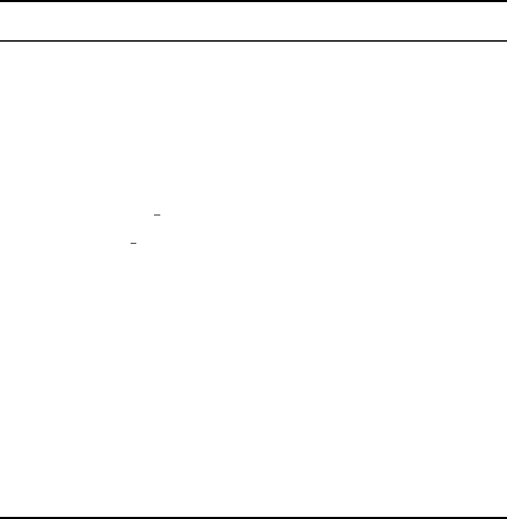
From Table 4.1, the highest F
n
SB
values obtained from I–V experiments can be plotted
vs ideality factor, as shown in Figure 4.4. Figure 4.4 indicates n values considerably larger
than unity, due to image force lowering, thermionic field emission, and lateral contact
inhomogeneity.
[38]
Higher F
n
SB
values for Zn-polar vs O-polar surfaces are also evident
from this plot, which features mostly air-exposed ZnO. UHV clean metal–ZnO contacts
also display higher F
n
SB
values for Zn-polar vs O-polar surfaces as well.
[9]
Note the high F
SB
values of Ag–Zn O even though the Ag work function of 4.26 eV is
much less than that of, e.g., 5.65 eV for Pt. This is attributed to the oxidation of Ag, which
increases the Ag work function substant ially.
[39]
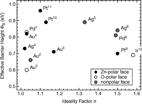
Allen et al. also investigated the effect of ZnO growth methods on the I–V character-
istics.
[35]
Figure 4.5 illustrates I–V plots for hydrothermal vs melt-grown ZnO as well as
their different polar or nonpolar surfaces.
The Influence of Surface Preparation on Schottky Barriers 93

Table 4.1 F
n
SB
measurements by various techniques vs orientation and crystal quality for
metals on ZnO surfaces prepared by different cleaning methods. The metal column includes
the corresponding work function. Reprinted from H.B. Michaelson, The work function of the
elements and its periodicity, J. Appl. Phys. 48, 4729. Copyright (1977) with permission from
American Institute of Physics
Metal qF
n
SB
(eV) Ideality
factor
Surface
treatment
Measurement
technique
Ref.
Pt (5.65) 0.75 nonpolar — Vac-cleave IPS [2]
Pt 0.42 (000
ı) 3.45 HD, ROP1A I–V [16]
Pt Ohmic (000
ı) NA LD, ATMA I–V [16]
Pt 0.39 (000
ı) 1.00 LD, ROP1A I–V [16]
Pt 0.61 (0001) 1.70 PLD, AG I–V [21]
Pt 0.85, 0.73 (0001) 1.77 ATMA, LA C–V, I–V [22]
Pt 0.96 (0001) 1.1 OCA I–V [23]
Pt 0.6 (0001) 3.1 OCA I–V [23]
Pt 0.70 (0001) 1.5 UVOA I–V [28]
Pt 0.93, 0.89 (0001) 1.15 HPA C–V, I–V [32]
Pt 0.55 (0001) 2.0 CCA I–V [33]
Pt 0.72, 0.68 (000
ı) 1.2 CCA C–V, I–V [33]
Ir (5.27) 0.65 (000
ı) 2.62 HD, ROP1A I–V [16]
Ir 0.69 (000
ı) 1.58 HD, ROP1A I–V [14]
Ir 0.54 (000
ı) 1.66 LD, ATMA I–V [16]
Ir 0.64(000
ı) 1.36 LD, ROP1A I-V [14]
Pd (5.12) 0.68 nonpolar — Vac-cleave IPS [2]
Pd 0.59,0.61,0.60 — Acid etch IPS, C–V, I–V [12]
Pd 0.73, 0.53 (0001) 1.3 ROP2 C–V, I–V [9]
Pd 0.68, 0.61 (000
ı) 1.2 ROP2 C–V, I–V [9]
Pd 1.14, 0.81 (0001)
PLD
1.49 AG C–V, I–V [24]
Pd 0.74 (0001) 2.0 Acetone
Acid etch
I–V [25]
0.60 (0001) 1.4 I–V
Pd 0.83 (000
ı) 1.03 HPA I-V [26]
Pd 1–1.2 (000
ı) 1.8 HPA C–V, I–V [27]
Pd 0.55 (0001) 2.0 CCA I–V [33]
Pd 0.59, 0.59 (000
ı) 1.2 CCA I–V, C–V [33]
Au (5.1) 0.65 nonpolar — Vac-cleave IPS [2]
Au 0.645,0.67,0.66 – — CCA IPS, C–V, I–V [12]
Au 0.67,0.60 (000
ı) 1.86,
1.03
ROPHT, ROPRT I–V [13]
Au 0.71 (0001),
0.60 (000
ı)
1.17,
1.03
ROPHT,
ROPRT
I–V [31]
[31]
Au Ohmic (0001) NA LD, ATMA I–V [2]
Au 1.2, 0.81 (0001) 1.2 LD, ROP2 C–V, I–V [9]
Au 1.07, 0.77 (000
ı) 1.3 LD, ROP2 C–V, I–V [9]
Au 0.48 (000
ı) 1.30 LD, ROP1A I–V [14]
Au Ohmic (000
ı) NA LD, ROP1, 650
C I–V [15]
Au 0.43 (000
ı) 3.57 HD, ROP1A I–V [14]
Au 0.46 (000
ı) 1.56 LD, ATMA I–V [14]
Au 0.48 (000
ı) 1.30 LD, ROP1A I–V [16]
Au Ohmic (0001) NA ATMA I–V [17]
Au 0.63 (0001) 1.15 HPA I–V [17]
Au 0.65 (0001) — ATMA C–V [18]
94 ZnO Surface Properties and Schottky Contacts
Here F
SB
values decrease with increasing n, due to inhomogeneity that produce a
distribution of barrier heights as well as tunneling contributions to the transport. Barriers
with n values approaching unity are considerably higher than those for conventional
nonideal contacts. Also Ag oxide contacts exhibit higher F
SB
for Zn-polar vs O-polar
surfaces similar to those reported for ele mental metals.
Barrier inhomogeneity can also account for the difference between barriers measured by
I–V vs C–V. Von Wenckstern et al. have compared effective barrier heights F
SB, eff
for
Table 4.1 (Continued)
Metal qF
n
SB
(eV) Ideality
factor
Surface
treatment
Measurement
technique
Ref.
Au 0.66 (0001) ZnO:N 1.8 OCA I–V [20]
Au 0.37 (000
ı) ZnO:N 3.5 OCA I–V [20]
Au 0.71, 0.70 (0001) 1.4 CCA I–V, C–V [33]
Au 0.70, 0.69 (000
ı) 1.1 CCA C–V, I–V [33]
PEDOT:PSS
(5.0)
0.9, 0.7 (0001) 1.2 HT, CCA I–V, C–V [36]
Ti (4.33) G0.3 nonpolar — Vac-cleave I–V [2]
Ti Ohmic (0001) NA OCA I–V [29]
Cu (4.65) 0.45 nonpolar — Vac-cleave I–V [2]
Al (4.28) 0.0 nonpolar — Vac-cleave I–V [2]
Ag (4.26) 0.68 nonpolar — Vac-cleave IPS [2]
Ag 0.92,0.89(11
20) 1.33 AG C–V, I–V [19]
Ag 0.69 (0001) — ATMA C–V [18]
Ag 0.84 (11
20) 1.5 O
2
plasma I–V [30]
Ag 0.80, 0.78 (0001) 1.2 CCA C–V, I–V [33]
Ag 1.11, 1.08 (0001) 1.08 CCA highest I–V, C–V [34]
Ag 0.80, 0.77 (000
ı) 1.1 CCA C–V, I–V [33]
Ag 0.99, 0.97 (000
ı) 1.06 CCA highest I–V, C–V [34]
Ag oxide
(5.0)
1.20, 0.93 (0001) 1.03 HT, OCA, OPS I–V, C–V [35]
Ag oxide 0.99, 0.79 (000
ı) 1.04 HT, OCA, OPS I–V, C–V [35]
Ag oxide 1.03 (0001) 1.14 MG, OCA,OPS I–V [35]
Ag oxide 0.98, 0.89 (000
ı) 1.10 MG, OCA,OPS I–V, C–V [35]
Ag oxide 1.02 M-plane 1.10 MG, OCA,OPS I–V [35]
Ta (4.25) Ohmic (000
ı) NA ROP1A I–V [15]
Ta Blocking (000
ı) NA LD, ROP1A,
350
C
I–V [15]
Ta Blocking (000
ı) NA LD, ROP1A,
550
C
I–V [15]
Ta Ohmic (000
ı) NA HD, ROP1A I–V [15]
Leaky (000
ı) NA HD, ROP1A,
550
C
I–V [15]
In (4.12)) G0.3 nonpolar — Vac-cleave I–V [2]
Crystal quality:Low defect (LD); high defect (HD); pulsed laser deposited (PLD); hydrothermal (HT); melt-grown (MG).
Surface treatment: Vacuum cleaved in stream of evaporating metal (Vac-cleave); H
3
PO
4
, HCl, deionized water (Acid
etch); chemically cleaned and air-exposed (CCA); laser annealed (LA); remote oxygen plasma cleaned at high temperature
(ROPHT), plus room temperature re-exposure (ROPRT); room temperature remote oxygen plasma for 1 h and air exposure
(ROP1A) or for 2 h without breaking vacuum (ROP2); hydrogen peroxide and air exposed (HPA); acetone, trichloroethy-
lene, methanol and air-exposed (ATMA); organic clean and air exposed (OCA); UV ozone and air-exposed (UVOA);
oxygen-plasma sputtered (OPS); as-grown (AG).
Measurement technique: Internal photoemission spectroscopy (IPS); current–voltage (I–V); capacitance–voltage (C–V).
The Influence of Surface Preparation on Schottky Barriers 95
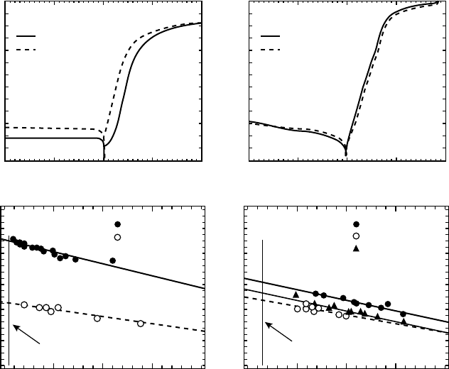
Pd on ZnO measured by I– V with barriers measured by C–V, F
SB, CV
.
[40]
Figure 4.6(a)
illustrates F
SB, eff
, F
SB, CV
and their difference (inset) vs temperature.
Lateral fluctuations in F
SB
can be modeled by a Gaussian distribution of barrier heights
with a standard deviation s around a mean value F
SB0,m
(for zero bias) according to:
[41]
F
SB; eff
ðTÞ¼F
SB0;m
ðTÞqs
2
=2k
B
T ð4:3Þ
The Figure 4.6(a) inset line yields s. Figure 4.6(b) shows the variation of F
SB, eff
with 1/T,
which should be linear if s in Equation (4.3) is temperature independent. Both F
SB0,m
and
s can vary with applied voltage V
A
with proportionality factors r
2
and r
3
, respectively,
according to:
F
SB;m
¼ F
SB0;m
þr
2
V
A
ð4:4aÞ
and
s
2
¼ s
2
0
þr
3
V
A
ð4:4bÞ
such that the ideality factor is given (for temperature-independent r
2
and r
3
) as:
n ¼ 1=½1r
2
þer
3
=ð2k
B
TÞ ð4:5Þ
The slope and straight line fits in Figure 4.6(b) yield r
2
and r
3
. In this Pd study,
s ¼(125 15) meV.
[24]
This approach provides a method for quantifying the homogene-
ity of Schottky barriers.
Pearton et al. have reviewed Schottky barriers to chemically treated ZnO and noted that
barrier heights do not seem to follow the difference in metal work functions.
[42]
They identified Au and Ag contacts on epiready ZnO(0001) surfaces cleaned with just
Figure 4.4 N-type barrier height F
n
SB
vs ideality factor n for the highest reported barriers on
ZnO. Reprinted from M.W. Allen, S.M. Durbin, and J.B. Metson, Silver oxide Schottky contacts
on n-type ZnO, Appl. Phys. Lett. 91, 053512. Copyright (2007) with permission from American
Institute of Physics
96 ZnO Surface Properties and Schottky Contacts
organic solvents as Schottky contacts with the lowest reverse current values. However, the
low thermal stability of these cont acts to ZnO limits their use in device applications.
As already mentioned, high work function metal s exhibit lower than expected F
n
SB
based
on a ZnO electron affinity x
ZnO
¼4.2 eV. Highest Au F
n
SB
were measured for ROP-cleaned
surfaces of low defect (LD) density ZnO. Highest Pd F
SB
were measured for hydrogen
peroxide oxidized surfaces. The increased barrier with oxidized interfacial layers indicates a
dipole contribution to F
SB
. Similarly, the blocking contact formed at the Ta–ZnO interface
indicates the formation of a Ta oxide layer.
[14,15]
Indeed, cathodoluminescence (CL) spectra
of the Ta–ZnO interface reveal the presence of a Ta
2
O
3
-like layer. On the other hand, H
diffusion can form a dipole at the Pd–ZnO interface that lowers F
SB
.
[9]
4.4 The Influence of Defects on Schottky Barriers
While many barrier variations can be ascribed to interface preparation, other extrinsic
factors appear to play a role. Only recently have factors such as crystalline
Ideality Factor (n)
Effective Barrier Height Φ
B
(eV) Current Density J
s
(A cm
–2
)
T = 300 K
Voltage (V)
HT-1 Zn-polar
HT-1 O-polar
T = 300 K
T = 300 K
(c)
(a)
HT-1 Zn-polar
HT-1 O-polar
image force controlled n
d
1.0
1.3
1.2
1.1
1.0
0.9
0.8
1.1 1.2 1.3 1.4
–2
10
0
10
–2
10
–4
10
–6
10
–8
10
–10
10
–12
–1 0 1 2
Ideality Factor (n)
T = 300 K
(d)
PM-1 Zn-polar
PM-2 O-polar
PM-3 s-plane
image force controlled n
d
1.0
1.3
1.2
1.1
1.0
0.9
0.8
1.1 1.2 1.3 1.4
Voltage (V)
PM-1 Zn-polar
PM-2 O-polar
(b)
–2
10
0
10
–2
10
–4
10
–6
10
–8
10
–10
10
–12
–1 0 1 2
Figure 4.5 Room temperature I–V characteristics (a, b) and effective F
SB
values vs ideality
factors (c, d) for silver oxide diodes on hydrothermal and melt bulk ZnO and for different
surface orientations. Reprinted from M.W. Allen, S.M. Durbin, and J.B. Metson, Silver oxide
Schottky contacts on n-type ZnO, Appl. Phys. Lett. 91, 053512. Copyright (2007) with
permission from American Institute of Physics
The Influence of Defects on Schottky Barriers 97
quality, impurity content, and native point defect conce ntration become serious
considerations.
In this regard, Schottky barrier measurements should take into account the fact that the
quality of ZnO crystals can vary dramatically, depending on the growth method, annealing
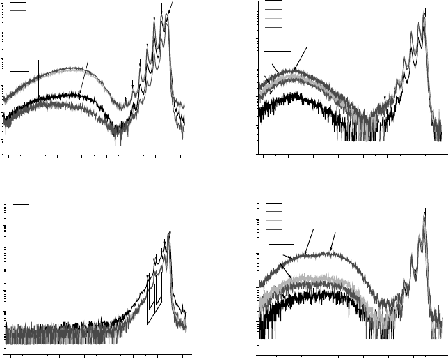
conditions, and subsequent polishi ng or etching. Figure 4.7 displays four examples of
DRCLS spectra taken from ZnO crystals grown from the melt or by hydrothermal
methods.
[43]
Each low temperature spectrum contains near band edge features including
phonon replicas as well as broad deep level features at 2.1 and 2.4 eV.
The depth U
0
of peak electron–hole pair creation rate varies with incident beam energy
E
B
such that U
0
¼55, 85, 300 and 990 nm for E
B
¼2, 5, 10 and 20 keV, respectively, for
the bare ZnO surface. Figure 4.7(a) and (b) are from the same crystal grower yet near band
edge (NBE) emission in (a) is an order of magnitude higher but has a much less uniform
distribution of deep level defects at 2.1 and 2.4 eV than in (b). Specifically, deep level
emission in Figure 4.7(a) increases by nearly two orders of magnitude between the near-
surface and the bulk. NBE emission in Figure 4.7(c) is even higher than in (a) plus there is
no measurable deep level emission. In contrast, Figure 4.7(d) shows DRCL spectra from a
hydrothermal crystal grown by a different vendor from (a) and (b) that exhibits orders of
magnitude lower NBE, high deep level emissions, and significant lower uniformity with
depth. This figure shows that defect concentrations can vary by orders of magnitude, not
only from different growers but also with depth on a nanometer scale.
To illustrate the effect of native point defects on I–V features, Figure 4.8 shows how
contacts to remote oxygen plasma (ROP)-cleaned ZnO(000
I) surfaces can change from
ohmic to Schottky-like as surface impurities and sub-surface native point defects are
removed. The contributions of surface contamination, sub-surface H, and native point
defects can be separated at different stages of this conversion process. As in Figure 4.3,
DRCLS of a ZnO surface shows that the 2.5 eV increases proportionally as excitation
Figure 4.6 (a) Effective barrier height F
SB, eff
, F
SB, CV
and F’
SB, CV
vs temperature for Pd/ZnO
(0001). The inset shows the difference between F
SB, eff
and F’
SB, CV
with the line through the
origin yielding the standard deviation s. (b) F
SB, eff
and 1/n-1 vs 1/T. Reprinted from H. von
Wenckstern, Mean barrier height of Pd Schottky contacts on ZnO thin films, Appl. Phys. Lett.
88, 092102. Copyright (2006) with permission from American Institute of Physics
98 ZnO Surface Properties and Schottky Contacts
occurs closer to the surface. Figure 4.8(a) illustrates this increase in the I(2.5 eV)/I
(3.36 eV) ratio vs depth of peak excitation rate.
[15]
It also shows the strong decrease of this
ratio with ROP treatment within the outermost few tens of nanometers.
Furthermore, this defect ratio continues to decrease even after 30 min ROP processing,
which XPS and low-energy electron diffraction measurements show cleans the surface
completely. Figure 4.8(b) shows the effect of these treatments. Au diodes on the as-
received surface are ohmic. With 30 min ROP surface cleaning, the I–V characteristic
becomes asymmetric with F
n
SB
¼0.44 eV and ideality n H 5. Additional ROP p rocessing
further increases rectification: F
n
SB
increases to 0.51 eV while n decreases to 1.51. Such
studies show that sub-surface defects rather than surface contaminants determine the
Schottky barrier changes.
Hydrogen within ZnO can act as donors, as predicted theoretically
[44]
and observed
experimentally,
[45,46]
which in turn can lead to heavy n-type doping that narrows the
surface space charge region and promotes tunneling. This is evident from
the ohmic contact (straight line) formed on ZnO exposed to a remote H plasma in
Figure 4.8(b).
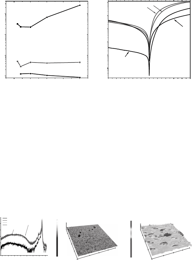
3.50
3.25
3.00
2.75
2.50
2.25
2.00
1.75
10
100
1000
10000
100000
1000000
85
55
330
3.092 eV
2.945 eV
3.021 eV
3.163 eV
3.233 eV
3.306 eV
Hydrothermal
2.4 eV
2.1 eV
Cathodoluminescence Intesity (a.u.)
Photon Energy (eV)
2KeV
5keV
10keV
20KeV
3.370 eV
U
o
(nm)
990
3.50
3.25
3.00
2.75
2.50
2.25
2.00
1.75
1
10
100
1000
10000
100000
~ 3.0 eV
330
990
85
Hydrothermal
~ 2.1 eV
Cathodoluminescence Intesity (a.u.)
Photon Energy (eV)
2KeV
5keV
10keV
20KeV
U
o
(nm)
55
3.370 eV
3.50
3.25
3.00
2.75
2.50
2.25
2.00
1.75
1
10
100
1000
10000
100000
1000000
1E7
56
70 meV
72 meV
3.147 eV
3.163 eV
3.217 eV
3.233 eV
3.289 eV
Melt-Grown
Cathodoluminescence Intesity (a.u.)
Photon Energy (eV)
2KeV
5keV
10keV
20KeV
Phonon
replica
splitting
3.320 eV
56
3.370 eV
3.503.253.002.752.502.252.001.75
1
10
100
1000
10000
Hydrothermal
~ 2.4 eV
~ 2.1 eV
Cathodoluminescence Intesity (a.u.)
Photon Ener
g
y (eV)
2KeV
5keV
10keV
20KeV
U
o
(nm)
55
85
330
990
3.370 eV
(a) (b)
(c) (d)
Figure 4.7 10 K DRCL spectra of ZnO crystals from the same supplier (a) and (b) grown
hydrothermally, (c) melt growth, and (d) grown hydrothermally by a second vendor. All
spectra recorded at constant power and optical resolution
The Influence of Defects on Schottky Barriers 99
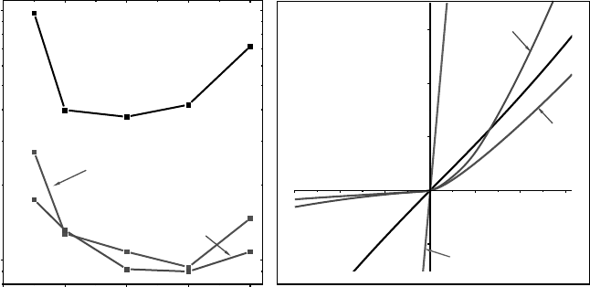
Figure 4.9 further illustrates how the density of native point defects within the ZnO
crystal before metallization strongly affects Schottky barriers. Figure 4.9(a) shows
I(2.5 eV)/I(3.36 eV) DRCLS intensity ratios for ROP-cleaned ZnO crystals with ”high”,
”medium” and ”low” defect concentrations. Figure 4.9(a) shows that the defect ratios can
vary by over two orders of magnitude for different ZnO crystals.
[14]
Figure 4.9(b) shows that the reverse currents vary by two orders of magnitude for Au
contacts to these surfaces. ”High” defect ZnO shows nearly ohmic behavior, ”medium”
defect ZnO shows only weak rectification, while the strongest rectification appears for the
“low” defect ZnO. In general, F
n
SB
are higher for “low” vs “high” defect ZnO crystals with
correspondingly lower ideality factors.
[14]
The direct correlation between reverse current
leakage and defect density underscores the importance of using low defect crystals in
Schottky barrier research.
The presence of defects and other electrically active sites are strongly affected by
surface preparation as well. Besides the defect variations with depth into the surface
space charge regions shown in Figure 4.7, sizeable variations in ZnO surface potential
are evident that depend sensitively on surface cleaning and polishing. In Figure 4.10(a),
DRCLS spectra show relatively low defect emissions within 40 nm of the free surface
but orders-of-magnitude higher defects deeper into the crystal.
[47]
This reduction is due
to a chemomechanical polishing that achieves near-monolayer surface roughness as
pictured in the AFM map in Figure 4.10(b). Notwithstanding this apparently smooth
surface, a KFPM map obtained simultaneously with the AFM map shows surface
43210
10
1
10
2
I (2.5 eV) / I(NBE)
Electron Beam Energy (keV)
(a)
(b)
-1.5 -1.0 -0.5 0.0 0.5 1.0 1.5
-1.0 x 10
-3
0.0
1.0 x 10
-3
2.0 x 10
-3
3.0 x 10
-3
H
2
Plasma
AR
60 min O
2
Plasma
φ
B
= 0.51
n =1.57
30 min O
2
Plasma
φ
B
= 0.44
n > 5
60 min. O
2
plasma
AR
30 min. O
2
Plasma
V (Volts)
Current (A)
Figure 4.8 (a) DRCLS ratio I(2.5 eV)/I(3.36 eV) vs depth of peak excitation vs ROP treatment
time. (b) I–V characteristics of Au/ZnO(000
I) diodes on these surfaces change: (i) as-received
and chemically etched (AR); (ii) with 30 min ROP cleaning; (iii) 60 min ROP cleaning; and (iv)
subsequent H plasma exposure. Reprinted from L.J. Brillson, et al., Dominant effect of near-
interface native point defects on ZnO Schottky barriers, Appl. Phys. Lett. 90, 102116. Copyright
(2007) with permission from American Institute of Physics
100 ZnO Surface Properties and Schottky Contacts
potentials that vary by well over 100 meV on the same surface on a scale of hundreds of
nanometers. In general, one finds larger variations in potential across otherwise smooth
surfaces in crystals with relatively high DRCLS defect emissions below the surface.
Such potential variations are even larger for surfaces with larger rms roughness and
surface asperities.
[47]
Similar pote ntial variations across hundreds of nanometers in other
crystals can easily account for the distribution of Schottky barrier heights discussed in
Figure 4.6.
(a)
(b)
(c)
3.50
0
0
2.5
5
7.5
10
2
2.5
5
µm
7.5
4
6
8
0
0
2.5
5
15
10
µm
µm
µm
3.25
3.00
2.75
2.50
2.25
2.00
1.75
1
10
100
1000
10000
100000
Constant power, slit width 0.25mm
2.5 eV
2.1 eV
Cathodoluminescence Intesity (a.u.)
Photon Energy (eV)
2KeV
5keV
10keV
20KeV
rms ~ 0.663 nm
mV
mV
450
425
400
375
350
325
450
425
400
375
350
325
nm
nm
8
8
6
0
-6
-8
4
0
-4
-8
Hydrothermal
Figure 4.10 (a) DRCLS of chemomechanically polished ZnO(000
1). (b) AFM surface topog-
raphy map of the same crystal with corresponding root mean square (rms) roughness. (c)
Simultaneously acquired Kelvin force probe microscope (KFPM) map. Reprinted from D.R.
Doutt, et al., Impact of near-surface native point defects, chemical reactions, and surface
morphology on ZnO interfaces. J. Vac. Sci. Technol. B. 26, 1477. Copyright (2008) with
permission from American Vacuum Society
20
15
10
5
0
0.01
0.1
1
10
2.0
1.6
1.2
0.8
0.4
0.0
-0.4
-0.8
-1.2
-1.6
-2.0
1E-6
1E-5
1E-4
1E-3
0.01
0.1
ZnO, Low Defect
ZnO, Medium Defect
ZnO, High Defect
I(2.5 eV) / (NBE)
Electron Beam Voltage E
B
(keV)
(a)
Low Defect
High Defect
Medium Defect
Current (A)
Voltage (V)
(b)
Figure 4.9 (a) Defect-to-NBE intensity ratio vs depth for “high”, “medium” and “low” defect
density ZnO. (b) Corresponding I–V characteristics. Reprinted from L.J. Brillson, et al.,
Dominant effect of near-interface native point defects on ZnO Schottky barriers, Appl. Phys.
Lett. 90, 102116. Copyright (2007) with permission from American Institute of Physics
The Influence of Defects on Schottky Barriers 101