Li S.Z., Jain A.K. (eds.) Encyclopedia of Biometrics
Подождите немного. Документ загружается.


device used to digitize the signal. Even though solid
state sensors are used in digital cameras, they pro-
duce an analog video signal. As a consequence, the
captured image resolution strongly depends on
the sampling frequency of the digitization device.
Other factors affecting the image resolution are the
file standard format adopted for the image storage
and the image processing application required to
postprocess the face images.
2. Responsivity. The amount of signal the sensor
delivers per unit of input optical energy. CMOS
imagers are marginally superior to CCDs, in gen-
eral, because gain elements are easier to be place on
a CMOS image sensor. This affects the illumina-
tion level required to capture a face image with a
sufficient contrast level.
3. Dynamic range. The ratio of a pixel’s saturation
level to its signal threshold. CCD sensors are
much better than CMOS in this regard. Some
CMOS sensors deliver 8 bit per pixel intensities,
corresponding to 128 real level variations. As
a consequence, the information content in the
image features is half than what is expected. A
higher dynamic range implies a higher image con-
trast even at low illumination levels and the possi-
bility to grab finer details. A gray level quantization
of 8 bit per pixel is generally sufficient for capturing
good quality face images. The sensor dynamic range
can be crucial when acquiring color images. In this
case, the color quantization may influence the in-
formation content in the face image itself, especially
if a low bit rate (with less than 8 bit per color
channel) is used for color coding.
4. Sensitivity to noise (signal to noise ratio – SNR).
The three primary broad compone nts of noise in a
CCD imaging system are photon noise (results
from the inherent statistical variation in the arriv-
al rate of photons incid ent on the CCD), dark
noise (arises from statistical variation in the num-
ber of electrons thermally generated within the
silicon structure of the CCD), and read noise (a
combination of system noise components inher-
ent to the process of converting CCD charge car-
riers into a voltage signal for quantification, and
the subsequent processing including the analog-
to-digital (A/D) conversion). A further useful
classification distinguishes noise sources on the
basis of whether they are temporal or spatial.
CCDs still enjoy significant noise advantages
over CMOS imagers because of qu ieter sensor
substrates (less on-chip circuitry), inherent toler-
ance to bus capacitance variations, and comm on
output amplifiers with transistor geometries that
can be easily adapted for minimal noise.
5. Uniformity. The consistency of response for differ-
ent pixels under identical illumination conditions.
Spatial wafer processing variations, particulate
defects, and amplifier variations create nonuni-
formities in light responses. It is important to
make a distinction between uniformity under illu-
mination and uniformity at or near dark. CMOS
imagers were traditionally much worse than CCDs
under both regimes. New on-chip amplifiers have
made the illuminated uniformity of some CMOS
imagers closer to that of CCDs, sustainable as
geometries shrink. This is a significant issue in
high-speed applications, where limited signal
levels mean that dark nonuniformities contribute
significantly to overall image degradation.
6. Shuttering. The ability to start and stop exposure
arbitrarily. It is a standard feature of virtually all
consumer and most industrial CCDs, especially
interline transfer devices, and it is particularly
important in machine vision applications. CCDs
can deliver superior electronic shuttering, with
little fill-factor compromise, even in small-pixel
image sensors. Implementing uniform electronic
shuttering in CMOS imagers requires a number
of transistors in each pixel. In line-scan CMOS
imagers, electronic shuttering does not compro-
mise fill factor, because shutter transistors can be
placed adjacent to the active area of each pi xel.
In area-scan (matrix) imagers, uniform electronic
shuttering comes at the expense of fill factor,
because the opaque shutter transistors must be
placed in what would otherwise be an optically
sensitive area of each pixel. A uniform synchro-
nous shutter, sometimes called a nonrolling shut-
ter, exposes all pixels of the array at the same time.
Object motion stops with no distortion, but this
approach reduces the pixel area because it requires
extra transistors in each pi xel. Users must choose
between low fill factor and small pixels on a small,
less-expensive image sensor, or large pixels with
much higher fill factor on a larger, more costly
image sensor.
7. Sampling speed. This is an area in which CMOS
arguably delivers better performances over CCDs,
310
F
Face Device

because all camera functions can be placed on the
image sensor. With one die, si gnal and power
trace distances can be shorter, with less induc-
tance, capacitance, and propagation delays. To
date, CMOS imagers have established only modest
advantages in this regard, largely because of early
focus on consumer applications that do not de-
mand notably high speeds compared with the
CCD’s industrial, scientific, and medical applica-
tions. Both the sampling and shuttering speed are
important when capturing video streams of faces.
In this case, it is important to ensure the image
stability and minimize the motion smear induced
by either the motion of the camera or the face.
This requires to tune the camera sampling fre-
quency to the motion speed induced in the
image sequence. If the face is very close to the
camera, small motions can induce large and fast
displacements on the image, thus producing mo-
tion smear. At a larger distance (above 50 cm), a
standard sampling frequency of 50 or 60Hz is
generally sufficient. In many low-cost devices,
the sampling frequency depends on the time re-
quired to transmit the signal from the device to
the frame buffer. Therefore, only low resolution
images can be captured at high sampling frequen-
cies. On the other hand, if a high, nonstandard
sampling frequency is required to capture stable
images w ith fast motions, the reduced exposure
time requires a higher sensitivity of the sensor to
preserve a high SNR.
8. Windowing. One unique capability of CMOS tech-
nology is the ability to read out a portion of the
image sensor. This allows elevated frame or line
rates for small regions of interest. This is an enabling
capability for CMOS imagers in some applications,
such as high-temporal-precision face tracking in
the subregion of an image. CCDs generally have
limited abilities in windowing.
9. Antiblooming. The ability to gracefully drain loca-
lized overexposure without compromising with
the rest of the image in the sensor. CMOS generally
has natural blooming immunity. CCDs, on the
other hand, require specific engineering to achieve
this capability; many CCDs that have been devel-
oped for consumer applications do, but those de-
veloped for scientific applications generally do not.
10. Biasing and noise. CMOS imagers have a clear
edge in this regard. They generally operate with a
single bias voltage and clock level. Nonstandard
biases are generated on-chip with charge pump
circuitry isolated from the user unless there is
some noise leakage. CCDs typically require a few
higher-voltage biases, but clocking has been sim-
plified in modern devices that operate with low-
voltage clocks.
The camera optics determines the general image
deformation, the depth of the field, and the amount
of blurring in the image. The lenses must be chosen
carefully according to the acquisition scenario. The
▶ focal length must be set to provide a sufficient
▶ depth of field (DOF) to always keep the subject’s
face in focus. If the range of distances is very large, a
motorized lens can be used to dynamically keep the
face in focus. Otherwise, a shorter focal length lens,
with a larger depth of field, can be used at the expenses
of an increase in the image distortion.
A 2D camera can be modeled with several para-
meters [2], including the following:
1. The (X, Y, Z) position of the center of the camera
lens
2. The focal length
3. The orientation of the sensor’s plane
4. The apert ure or
▶ field of view (Xf, Yf )
5. The physical x and y dimensions of each pixel on
the sensor
6. The normal to the focal plane
7. The lenses properties
Many parameters can be neglected in the pin hole
camera model. This is a simplified model where the
physical parameters are reduced to five virtual para-
meters, namely the following:
1. The focal length F
2. The pixel width and height dx, dy
3. The x and y coordinates of the optical center (x
c
, y
c
)
Assuming the pin hole camera model, the (x, y) pro-
jection on the image plane of a 3D point (X, Y, Z) can
be represented as (refer to Fig. 1)
x ¼ F
x
X
Z
;
y ¼ F
y
Y
Z
;
ð1Þ
where F
x
and F
y
represent the two values of the
focal length, which take into account the image aspe ct
ratio.
Face Device
F
311
F

The pin hole model cannot take into account sev-
eral effects of the misalignment of the sensor with the
lenses, not the lens aberration or the image deforma-
tion due to the focal length. However, when high
accuracy is required or when low-end cameras are
used, additional effects have to be taken into account.
The failure of the optical system to bring all light rays
received from a point object to a single image point or to
a prescribed geometric position should then be taken
into account. These deviations are called aberrations.
Many types of aberrations exist (e.g., astigmatism, chro-
matic aberrations, spherical aberrations, coma aberra-
tions, curvature of field aberration, and distortion
aberration). It is outside the scope of this work to discuss
them all. The interested reader is referred to the work of
Willson [3] and to the photogrammetry literature [4].
Many of these effects are negligible under normal
acquisition circumstances. Radial distortion, however,
can have a noticeable effect for shorter focal lengths.
Radial distortion is a linear displacement of image po-
ints radially to or from the center of the image, caused
by the fact that objects at different angular distance
from the lens axis undergo different magnifications.
It is possible to cancel most of this effect by
▶ Face
Warping the image.
Active 2D Face Devices
Withinthegeneralclassof2Dfacedevices,activedevices
rely on the possibility to use an active source of energy to
radiate the subject’s face. Among them, the most com-
monly used are the near infrared cameras. These cameras
have normal optics but the sensor (either CMOS or
CCD) is sensitive to a wavelength spectrum between 0.7
and 1.1 mm. To perform image acquisition, the subject’s
face to be captured must be illuminated by an infrared
illuminator. Given the sensitivity response curve of the
near infrared sensor, the pixel intensities are almost ex-
clusively due to the reflection of the infrared light on the
face skin. An example is presented in Fig. 2. As a conse-
quence, a remarkable advantage of this face acquisition
device is the relative insensitivity to changes in envi-
ronmental illumination.
3D Face Devices
Another category of face device are those aimed at
acquiring the 3D shape information of the face. There
are several technologies applied to produce 3D cameras
for face acquisition. They can be broadly grouped in
the following categories:
1. Stereo triangulation cameras.A pair of stereo
camerasisusedfordeterminingthedepthto
points on the face, for example, f rom the center
point of the line be tween t heir focal points.
To solve the depth measurement problem using
stereo cameras, it is necessary to first find
corresponding points in t he two i mages. Solving
the correspondence problem is one of the main
problem when using this type of technique. As a
consequence, range imaging based on stereo tri-
angulation can usually produce reliable depth
estimates only for a s ubset of all points visible
in both cameras. The advantage of this tech-
nique is that the measurement i s more or less
passive; it does not require special arrangements
in terms of scene illumination.
2. Light stripe triangulation. Illuminating the face
with a light stripe creates a reflected line as seen
from the light source. From any point out of the
plane of the stripe, the line will typically appear as a
curve, the exact shape of which depends both on
the distance between the observer and the light
source and on the distance between the light source
Face Device. Figure 2 Sample image acquired with a
near-infrared camera.
312
F
Face Device

and the reflected points. By observing the reflected
sheet of light using a camera (often a high resolution
camera) and knowing the positions and orienta-
tions of both camera and light source, it is possible
to determine the distance between the reflected
points and the light source or camera. By moving
either the light source (and normally also the cam-
era) or the scene in front of the camera, a sequence
of depth profiles of the scene can be generated.
These can be represented as a 2D range image.
The most common cameras are based on the pro-
jection of an invisible and unh armful laser light
stripe. The light stripes projected along the face
surface are captured by a conventional camera.
The distortion in the light stripes induced by the
face shape is computed to infer the 3D structure of
the surface.
3. Time-of-flight laser scanner. The time-of-flight 3D
laser scanner is an active scanner that uses laser
light to probe the subject. At the hear t of this type
of scanner is a time-of-flight laser range finder. The
laser range finder finds the distance of a surface
by timing the round-trip time of a pulse of light.
A laser is used to emit a pulse of light and the
amount of time before the reflected light is seen
by a detector. Since the speed of light c is known,
the round-trip time determines the travel distance
of the light, which is twice the distance between the
scanner and the surface.
Inspite of the camera and sensor technology, the pro-
duced image is either a depth map, a collection of 3D
points in space, or a set of 3D features representing the
3D structure of the acquired face. A sample depth map
of a face is shown in Fig. 3. The most frequently used
representations for the acquired 3D data can be listed
as follows:
1. Point cloud. A large number of 3D points that are
sampled from the surface of the face are stored.
2. 3D mesh. Triangulation is used to produce a mesh
from the point cloud. This is a more compact
representation. Range images – One or more 2D
range images can be stored, especially if the range
data are taken from a single perspective.
3. Feature sets. There are different features that one
can derive and store for each face. Typical features
are landmark locations (nose tip, eyes, corners of
the mouth, etc.), surface normals, curvatures, pro-
file features, shape indices, depth and/or colour
histograms, edges, and subspace projection coeffi-
cients (PCA and LDA are frequently used).
The point cloud representation is the most primitive 3D
information provided by a 3D camera. The 3D-RMA is
an example of a database of 3D face models represented
by clouds of points [6]. For long time, it has been the
only publicly available database, even if its quality is
rather low. Meshes are obtained by triangulation.
These are more structured and easier to deal with.
Data in the form of meshes are more available today,
but in most cases the mesh databases are proprietary.
Usually, more than one representation is used in a
single algorithm. Texture information, if available, is
generally stored for each 3D point or triang le. A sam-
ple 3D face image with the associated reflectance
map is shown in Fig. 4.
Summary
A face device is a system to acquire a set of digital data
samples representing a human face. As the human face
is a complex 3D object, the data can be in several
forms, from a 2D image to a complex 3D representa-
tion. The principal component of a face dev ice is a
digital camera, which acquires images either for a
direct 2D representation or to build a 3D representa-
tion of the face shape. Different cameras offer variable
performances, in terms of quality of the signal,
Face Device. Figure 3 Sample depth face image. The
gray levels are inversely proportional to the distance of
the face surface from the camera [5].
Face Device
F
313
F

sensitivity to different light spectral components, and
capturing speed. The proper imaging device must be
carefully chosen for the application scenario. The
ambient illumination level, the required level of detail,
the effects of noise, and the motion speed of the objects
in the scene must all be carefully considered.
Related Entries
▶ Acquisition
▶ Authentication
▶ Enrollment
▶ Identification
▶ Verification
References
1. Litwiller, D.: CCD vs. CMOS: facts and fiction. Photonics
Spectra, pp. 151–154 (2001)
2. Blais, F.: Review of 20 years of range sensor development.
J. Electron. Imaging 13(1), 231–240 (2004)
3. Willson, R., Shafer, S.: What is the center of the image? J. Opt.
Soc. Am. A 11(11), 2946–2955 (1994)
4. Slama, C.: Manual of Photogrammetry/ American Society of
Photogrammetry, Falls Church, VA, USA, 4th edn. (1980)
5. Phillips, J.J., Flynn, P., Scruggs, T., Bowyer, K.W., Chang, J.,
Hoffman, K., Marques, J., Jaesik, M., Worek, W.: Overview of
the face recognition grand challenge. In Proceedings CVPR05,
pp. 947–954 (2005)
6. Beumier, C., Acheroy, M.: Automatic 3D face authentication.
Image Vision Comput. 18(4), 315–321 (2000)
Face Identification
▶ Face Recognition, Thermal
▶ Forensic Evidence of Face
Face Image Data Interchange
Formats
▶ Face Image Data Interchange Formats,
Standardization
Face Image Data Interchange
Formats, Standardization
PATRICK GROTH ER ,ELHAM TABASSI
National Institute of Standards and Technology, USA
Synonym
Face image data interchange formats
Definition
Openly documented data structures for universally
interpretable interchange of facial imagery.
Face Device. Figure 4 Sample 3D face image and projected 2D intensity values from the face recognition grand
challenge (FRGC) [5] database.
314
F
Face Identification

Biometric data interchange standards are needed to
allow the recipient of a data record to successfully
process data from an arbitrary producer. This defines
biometric interoperability and the connotation of the
phrase ‘‘successfully process’’ is that the sample, in this
case, a facial image record, can be accurately identified
or verified. This can be achieved only if the data record
is both syntactically and semantically conformant to a
documentary standard.
Introduction
Facial image standards are perhaps the oldest docu-
mented biometric data standards. Predating even the
fingerprint, the facial image has been mandated for
identity documents since at least the World War I
when several European governments saw the need for
a facial photograph to ser ve as the core element in
the cross-border identity verification application. Of
course the data record was simply an analog paper
printed photograph - the advent of fully automatic
face recognition algorithms and the need for digital
images was at least 70 years distant [1, 2]. However the
intention remains the sam e: to support (human or
machine) verification of an individual via a high qual-
ity standardized image.
Roles
The use of face imager y for recognition is ubiquitous
in applications where a human does the recognition.
This rests on three factors: The ability of humans to
recognize faces; the almost universal availability of the
face In some cultures the face is covered or painted,
and in such cases modalities such as iris or hand
geometry are dominant.; and the availability of cam-
eras and printers . The result is that face images, printed
on passports, drivers’ licenses, credit cards, and other
tokens, have been the primary biometric element for
human verification for many years.
Nowadays with the advent and maturation of tech-
nologies for automated face recognition, the use of the
face for verification [3] is but one component of a
larger marketplace in which commercial systems have
been both piloted and fully deployed for identi fication
applications such as watch-list surveillance [4] and
duplicate detection (e.g., for drivers licenses, or visas).
In addition the law enforcement community has for
years taken mugshot images and, while these are often
only used for human identificat ion, they are being used
operationally [5].
The common theme among all is that recognition
accuracy is critically sensitive function of the quality of
the image, where quality here refers to the photometric
and geom etric properties of the image. The former
include contrast, exposure, and uniformity of lighting;
the latter refers to the size of the image and the angular
orientation of the face to the viewing direction. The
effect of non-idealities in these areas has been quanti-
fied extensively and there is an enormous literature
documenting research in how to improve the robust-
ness and invariance of the algorithms to variations in
these quantities. In parallel, there has been a concerted
effort by groups of vendors, users, governmental orga-
nizations, and academics to develop standards that
establish a baseline for the acquisition and quality of
the captured images.
It is no coincidence that the largest marketplace for
face recognition technologies today is in those applica-
tions where the quality is most highly controlled,
namely passpor ts and visas, where the photographers
and the subjects who pay them, are positively moti-
vated to provide good conformant images.
In a more general sense, formal face images stan-
dards also serve to do what many other data format
standards do: they define a parseable record that allows
syntactic interoperability. This creates a foundation for
a marketplace of off-the-shelf products, and is a neces-
sary condition to achieve supplier independence, and
to avoid vendor lock-in. It is perhaps surprising that in
a world where many raster image formats are open and
standardized [6–8] it remains common for images to
be retained in a fully proprietary (i.e., unpublished)
format. Such practice may be acceptable within an
application, but is a serious impediment once cross-
organizational interchange of data is required. This is
the essence of interoperabilit y which allows modular
integration of products without compromising archi-
tectural scope, and it facilitates the upgrade process
and thereby mitigates against obsolescence.
The business implications of these benefits are
many. A good standard, well implemented, may create
entirely new markets (e.g., e-Passports include face
image records). On the other hand, robust standards
tend to lead to competition and reduced profit mar-
gins. This process, commoditization, is an inhibitory
factor for many technology companies that balance the
Face Image Data Interchange Formats, Standardization
F
315
F

promise of new or expanded marketplaces against re-
duced barriers to entry for competitors. The decision is
determined by the amount of intellectual property that
a standard allows suppliers to hide behind its imple-
mentation. From the user perspective, standards may
serve to enhance competition and performance. For
example, face image standards (primarily ISO/IEC
19794-5 [9]), which are currently being mandated in
a number of large government and international pro-
grams, specify image formats without requiring partic-
ular equipment or matching algorithms.
This is the motivation for formal published con-
sensus standards.
Standards do not in and of themselves assure inter-
operability. Specifically, when a standard is not fully
prescriptive, or it allows for optional content, then
two implementations that are both exactly conformant
to the standard may still not interoperate. This situa-
tion may be averted by applying further constraints on
the application of the standard. This is done by means
of ‘‘application profile’’ standards which formally call
out the needed base stand ards and refine their optional
content and interpretation.
History of Face Standardization
The current face standards descend from standardiza-
tion efforts that began in the mid 1990s. These were
driven in large part by the needs of the United States’
Federal Bureau of Investigation who sought to estab-
lish uniform standards for State and local law enforce-
ment authorities submitting images to them.
Referring to Table 1, the first standard, approved in
April 1997, established the syntax of a record denoted
‘‘Type 10.’’ The image data it required was either in raw
grayscale format or, if compressed, in the then draft
JPEG/JFIF standard [6]. Concurrently NIST estab -
lished procedures for the geom etric and photometric
properties of images and published its recommenda-
tions in September 1997. These were extended and
modified, and incorporated, in 2000, into both the
American Association of Motor Vehicle Administra-
tors standard for drivers licenses, and the revision of
the FBI’s original biometric data specifications.
These standards formed the basis for the sub-
sequent development of the national INCITS 385:2004
standard in 2004, which in turn begat the full ISO/IEC
19794-5 International Standard in 2005. (At the time
of writing the standard is under amendment to regu-
late the acquisition process, and to establish a contain-
er for three dimensional data.) A substantially revised
standard which would include these changes (and
others) is likely to be completed late in the decade.
The ISO/IEC 19794-5 Face Image
Standard
The ISO/IEC 19794-5:2005 standard is the fifth part of
a multipart biometric data interchange format stan-
dard. The standard is organized by modality, and other
parts cover fingerprint images, irises, and hand geom-
etry among many others. The Part 5 standard is the
most widely implemented, most actively developed,
and most modern face standard. Its content drove the
Face Image Data Interchange Formats, Standardization. Table 1 The evolution of contemporary face image standards
Date Title of Standard
04/1997 Addendum To ANSI/NIST-CSL 1-1993 (adding Mugshots, scars, marks and tattoos)
09/1997 NIST Best Practice Recommendation for the Capture of Mugshots
06/2000 AAMVA National Standard for the Driver License/Identification Card
09/2000 ANSI/NIST-ITL 1-2000 - Data Format for the Interchange of Fingerprint, Facial, & Scar Mark & Tattoo
Information - Type 10
05/2004 INCITS 385:2004 - Face Recognition Format for Data Interchange
06/2005 ISO/IEC 19794-5:2005 - Face Image Data
04/2007 ANSI/NIST-ITL 1-2007 - Data Format for the Interchange of Fingerprint, Facial, & Other Biometric Information -
Type 10
06/2007 ISO/IEC 19794-5/Amd 1 - Conditions for Taking Photographs for Face Image Data
2009 (Est) ISO/IEC 19794-5/Amd 2 - Three Dimensional Face Image Data Interchange Format
316
F
Face Image Data Interchange Formats, Standardization

revision of the Type 10 record of the ANSI/NIST ITL
1-2007 described in section . While the ISO standard is
under revision, w ith publication due late in the decade,
the existing 2005 standard has been called out for some
major identity management a pplications. The fore-
most of these is the e-Passport, whi ch the International
Civil Aviation Organization formalized in its ICAO
9303 standard. This points to ISO/IEC 19794-5 as the
mandatory g lobally interoperable data element for
ISO/IEC 14443 contactless chip passports.
The face standard defines a binary record structure
for the storage of one or more face images. It estab-
lishes requirements on the syntax and semantic con-
tent of the structure. These requirements are stated in
terms of the following four categories.
Format: These requirements detail the syntactic
arrangement of the data elements in the record.
Scene: These requirements regulate variables such a
pose, expression, shadows on the face, the wearing
of eye glasses.
Photographic: These requirements concern correct
exposure of the subject, distortion, focus, and
depth of field.
Digital: The requirements include specifications for
dynamic range, color space, pixel aspect ratio, and
video interlacing.
The standard imposes these requirements incre-
mentally: Fig. 1 shows that the useful frontal image
types inherit from parent types and add require-
ments. This object oriented design allows for future
specialized types to be added, in cluding 3D frontal
types. In addition the standard establishes two geomet-
ric position specifications for the face. These are shown
in Fig. 2. The tighter specification, for known as the
token Frontal, requires detection of the eye coordinates
and of fine transformation of the image.
The record includes fields for expression, eye-color,
hair color, and gender. It optionally allows the inclu-
sion of ISO/IEC 14496-2 MPEG 4 feature points. The
standard includes various qualit y related requirements.
For example the pose angle is required to be 5deg,
and there must be at least 7 bits of greylevel informa-
tion on the face. Conformance to these requirements
will elevate face recognition performance. Once an
image is acquired a test of its conformance to the
standard’s specifications requires some non-trivial
Face Image Data Interchange Formats, Standardization. Figure 1 Inherited types of the ISO/IEC 19794-5 face image
standard.
Face Image Data Interchange Formats, Standardization
F
317
F
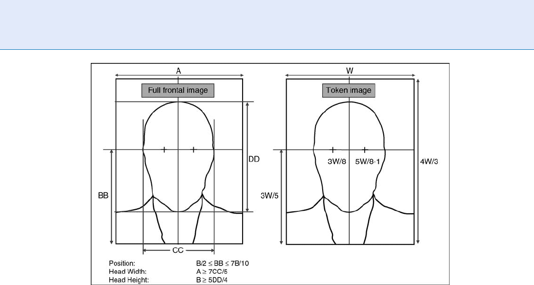
image analyses. A number of software products have
been developed to ‘‘box-check’’ ISO conformance and
to prepare the standardized record.
The ANSI/NIST ITL 1-2007 Type
10 Record
Since its initial development in the early 1990s, the so-
called ANSI-NIST standard has been very widely imple-
mented and used within and between the law enforce-
ment communities of the United States and the many
other countries. Its primary use is the transmission of
fingerprint data from the State and Local authorities to
central automated fingerprint identification systems,
primarily those operated by the Federal Bureau of Inves-
tigation. The ANSI/NIST standard includes defined
Types for the major biometric modalities. The standard
is multimodal in that it allows a user to define a trans-
action that would require, for example, fingerprint data
as Type 14, a facial mugshot as Type 10, and the man-
datory header and metadata records Type 1 and 2.
These are linked with a common numeric identifier.
Of concern here, since its development in 1997, is
the Type 10 record. It supports storage not just of face
images, but also those of scars, marks, and tattoos,
with the particular type of content being recorded in
the ‘‘image type’’ field of the header.
Unlike the ISO standard’s fixed binary structure, the
Type 10 has a tag-value structure in which a three letter
code begins a field. The mandatory fields are: Record
length, image designation code (identifier linking, say,
Type 14 finger + Type 10 face records), image type (face
or otherwise), the source agency (e.g., local police de-
partment), the capture date, the width, height and scan-
ning resolution, the compression algorithm, color space,
and the subject acquisition profile. This latter field
encodes, essentially, the conformance of the image to
particular capture specifications. These are either estab-
lished elsewhere [9–12] or introduced in the standard.
The optional fields are: pose category (frontal, pro-
file, other), actual pose angles, whether the subject was
wearing headwear or eyewear, the camera type, a quali-
ty value and it’s source, the eye and hair color, facial
expression, eye and nostril locations and MPEG 4 fea-
ture points, and whether the capture was attended or
automatic. The last field contains the image data itself,
which is either an uncompressed raw greyscale or color
image, or a JPEG, JPEG 2000 or PNG encoded image.
Amendment 1 to ISO/IEC
19794-5:2005
The 2007 amendment is an informative Annex to the
base 2005 face standard. It is written to provide expert
Face Image Data Interchange Formats, Standardization. Figure 2 Geometries of the ISO/IEC 19794-5 frontal face
images.
318
F
Face Image Data Interchange Formats, Standardization

guidance for the photography of faces particularly by
owners and operators of studios, photo stores or other
organizations producing or requiring either printed
photographs or digital images that would conform. It
is intended to assist in the production of images that
are conformant to the frontal type requirements of the
base standard.
The standard regulates the subject, lighting, and
camera placement for three kinds of face acquisition
environments listed here in the order of increasing
space constraints and n on-ideality : a photo studio
(e.g., for a passport), a registration desk (e.g., for a
driving license), and a photo-booth. For each of these
the standard addresses camera-subject positioning (in
terms of distance, height, focus, and depth o f field),
exposure (in terms of F-stops and shutter speed), and
illumination (in terms of number, ty pe and placement
of lights). The document also provides guidance on
printing and scanning of paper photographs.
Amendment 2 to ISO/IEC
19794-5:2005
A second amendment is currently under preparation.
This is aimed at standardizing a container and speci-
fications for images that include three dimensional
shape information of the human head. An initial
effort within the United States, INCITS 385:2004
Amendment 1, allowed a 2D face image to be accom-
panied by a z-axis range map (e.g., from a structured
light sensor). This shape information was recorded
as the intensity values in a greyscale PNG image. The
ISO standardization process has recently sought to
allow more complete 3D information including the abil-
ity to encode concavities and folded structures (e.g.,
hook nose).
The standards are also likely to allow the storage
of 3D information computed from 2D information
such as morphable models [13] and active appearance
models [14].
Resolution Requirements
The image sizes mentioned in ISO/IEC 19794-5:2005
are very much less than those attainable with contem-
porary consumer grade digital cam eras. The reasons
for this are two. First, the face recognition algorithms
of the early part of the decade were designed to operate
with an interocular eye distance of between 40 and
maybe 120 pixels. Second, the standard aims to be
application independent, i.e., to only establish a mini -
mum resolution to support automated face recogni-
tion. While more modern implementations are capable
of exploiting high resolution imagery, the images may
be too large for operational use (e.g., on an e-Passport
chip, where size is typically much lesser than 50KB).
Nevertheless, the 2007 revision of the ANSI/NIST ITL
1-2007 standard reflected the utility of high resolution
imagery by incorporating a laddered scale that culmi-
nates in an image with a width such that 1700 or more
pixels lie on the faces of 99% of U.S. male subjects. This
specification supports forensic analysis of the face. It is
termed Level 51 and is the highest level of the Type 10
record’s Subject Acquisition Profile stack.
Note that a separate profile standard or require-
ments document could normatively specify minimum
or maximum resolutions for a particular application.
For example, the PIV specification[11] requires that
imaging of a 20cm target at 1.5 metres produces
240 pixels, corresponding to about 90 pixels between
the eyes.
Note that no standard currently exists for the certi-
fication of face recognition imaging systems. Such a
standard might reasonably establish true resolution spe-
cifications in terms of line pairs per millimeter and as a
full modulation transfer function profile. This would
regulate the entire imaging system including the effects,
say, of video compression.
Standards Development
Organizations
Standards a re developed by a multitude of standards
development organizations (SDOs) operating in a
great variety of technical disciplines. SDO’s exist with-
in companies and governments, and underneath trade
associations and international body umbrellas. Inter-
national standards promise t o regulate larger mar-
ketplaces and the development process involves
more diverse and thoroug h review and so consensus
is more difficult to achieve. With stakes often hig h,
development processes are conducted according to
definitive sets of rules. These are intended to achieve
consensus standards that are legally defensible, imple-
mentable, and effective.
Face Image Data Interchange Formats, Standardization
F
319
F