Gupta D. (Ed.). Diffusion Processes in Advanced Technological Materials
Подождите немного. Документ загружается.


the thin-film metallization used in the interconnection technology of mod-
ern computers. Each driving force deserves an exhaustive discussion in its
own right, which may be found in earlier review articles by Shewmon,
[10]
Huntington,
[31]
and Tu.
[32]
Here, we discuss the case of the chemical com-
position variation that gives rise to chemical potential gradients in non-
ideal solid solutions. The phenomenon, though old, has assumed greater
significance in the context of recent development of the artificially lay-
ered thin films known as manmade superlattices and multilayered thin
films in general.
The atomic force over N lattice planes due to the chemical potential
gradient (∂m∂x) may be written as:
F
a
k
N
T
[ln C
2
g
2
ln C
1
g
1
], (43)
where γ
1,2
are the chemical activity coefficients for the non-ideal solution
and C
1,2
are the concentration terms; the subscripts 1 and 2 refer to the spe-
cific component of the binary solution. Despite the large variation of con-
centrations and activity factors (for example, 10 C
2
g
2
C
1
g
1
1000,
over, say, 10 atomic planes), the force factor remains small in view of its
logarithmic nature. Under these conditions, Eq. (42) can be simplified as:
a
kT
F
1, (44)
which is known as the linear region. Hence, the drift term in Eq. (1) can
be identified from its basic definition and random walk theory
[21]
as:
C
1
v C
1
a
2
FkT (45)
or
v
D
k
1
T
F
. (46)
The quantity D
1
kT is denoted by B
1
. In general, it is a tensor. Equation
(46) is commonly known as Nernst-Einstein relationship. For diffusion in
concentrated alloys that display non-ideal behavior, Fick’s first law for the
first component may then be expressed in a generalized form as:
J
1
B
1
FC
1
. (47)
22 DIFFUSION PROCESSES IN ADVANCED TECHNOLOGICAL MATERIALS
Ch_01.qxd 11/30/04 8:36 AM Page 22

DIFFUSION IN BULK SOLIDS AND THIN FILMS, GUPTA 23
For a multicomponent system where F
–
i
is the partial molal free energy of
the ith component, Eq. (47) assumes the form:
J
i
N
1
∂
∂
F
x
i
B
i
C
i
. (48)
From this generalized Fick’s first law and the non-ideal behavior of the
alloy, Darken derived the following equation for chemical diffusion:
[19]
D
∼
(D
1
∗
C
2
D
2
∗
C
1
)
1
d
d
l
l
n
n
C
g
1
1
, (49)
where D
1
*
and D
2
*
are the tracer diffusivities of the two components of
the alloy, and g
1
and g
2
are the chemical activity coefficients. The terms in
the square brackets are collectively known as the thermodynamic factor.
It should now be obvious that without the knowledge of the thermody-
namic factor, it is not possible to account fully for the observed chemical
diffusion. Only Boltzmann-Matano-type diffusion experiments, coupled
with marker velocity measurement alluded to in Sec. 1.2.1 [see Eqs. (21)
and (22)], fully account for chemical diffusion. In the regular-solution-
type alloys, the factor g is independent of the composition, but the ther-
modynamic factor still remains finite. Only in ideal solutions do g 1 and
the chemical diffusivities become identical with those obtained using the
tracer techniques. Note that Darken’s Eq. (49) accounted for uphill diffu-
sion against the composition gradients first observed in a Fe-0.4%C/Fe-
0.4%C-4%Si couple. The explanation of this effect is that addition of Si
increases the chemical potential of the Fe-C system.
[33]
This observation
underscores the fact that in the chemical diffusion, the basic driving force
is the chemical potential gradient, and in some limiting cases it becomes
the concentration gradient. The latter may be violated in the uphill diffu-
sion, which should be a common occurrence in thin-film metallic alloy
couples.
1.2.5 Nonlinear Chemical Diffusion Regime
When sharp chemical potential gradients exist over small distances,
10 atomic spacing, Eq. (42) cannot be simplified linearly since the
boundary condition in the inequality [Eq. (44)] is not satisfied. Such a sit-
uation arises in the spinodal decomposition of a single phase where the
curvature of the free-energy composition plot ∂
2
F∂C
2
becomes negative.
Ch_01.qxd 11/30/04 8:36 AM Page 23

Decomposition by uphill diffusion occurs as it lowers the free energy.
Other examples of the existence of sharp chemical potential are the artifi-
cially layered polycrystalline films investigation by Cook and Hilliard
[34]
and compositionally modulated amorphous thin films studied by
Rosenblum et al.
[35]
and by Greer and Spaepen.
[36]
The spinodal solid-state
transformation is known as continuous; that is, it does not involve any
nucleation and is assisted by diffusion that occurs under a sharp chemical
potential gradient. This subject is briefly discussed here. Cahn and
Hilliard
[37]
and the recent review article by Doherty
[38]
provide background
and in-depth discussion.
For spinodal decomposition, Doherty
[38]
has shown that the Darken’s
term is the controlling factor in determining the curvature of the free-
energy and composition given by:
∂
∂
C
2
F
2
RT
C
1
1
C
1
2
1
d
d
l
l
n
n
C
g
1
2
, (50)
where the notations have the same meaning as previously defined. We
only need to change the various chemical concentrations to keep them
consistent with those used by Doherty
[38]
so that C
1
1 C
2
1 C.
Combining Eqs. (49) and (50), the chemical diffusivity D
∼
in the spinodal
decomposition may be written as:
D
∼
[D
1
*
C
2
D
2
*
C
1
]
C
R
1
C
T
2
d
d
C
2
F
2
, (51)
and the diffusion mobility M
D
as:
M
D
[D
1
*
C
2
D
2
*
C
1
]
C
R
1
C
T
2
. (52)
To describe the thermodynamics of the inhomogeneous solid solution,
a correction term is introduced as:
d
d
C
F
inhomo
d
d
C
F
homo
2k
∂
∂
2
x
C
2
. (53)
Herein, k is the gradient-energy coefficient NkT
c
y
2
, where T
c
is the
critical temperature below which the homogeneous alloy tends to unmix
and y is the “interaction distance” of atoms.
[39]
24 DIFFUSION PROCESSES IN ADVANCED TECHNOLOGICAL MATERIALS
Ch_01.qxd 11/30/04 8:36 AM Page 24

DIFFUSION IN BULK SOLIDS AND THIN FILMS, GUPTA 25
From Eqs. (52) and (53), Fick’s two laws for the inhomogeneous solid
solution may be rewritten as:
J
∼
M
D
d
d
C
2
f
o
2
C 2M
D
k
∂
∂
3
x
C
3
(54)
and
d
d
C
T
M
D
f
o
∂
∂
2
x
C
2
2M
D
k
∂
∂
4
x
C
4
, (55)
where f
o
(dFdC)
homo
and f
o
∂
∂
C
f
o
2
.
The nonlinear differential equation above has been solved by Cahn
and Hilliard
[37]
and Cahn
[39, 40]
for spinodal decomposition. An important
spinoff from this theory has been the understanding of diffusion at low
temperatures in compositionally modulated thin films, as discussed by
Cook and Hilliard.
[34]
Accordingly, a harmonic composition modulation C(t) will grow or
decay with time t as:
C C
0
A
0
exp [D
∼
l
h
2
t]cosh x, (56)
where C
0
is the average composition, A
0
is the initial amplitude of the
modulation, h(2pl) is the wave number, and D
∼
l
is the effective inter-
diffusivity. The macroscopic interdiffusivity and D
∼
l
are related as:
D
∼
l
D
∼
[1 2kh
2
f
0
]. (57)
For small deviations from homogeneity D
∼
, f
0
, and k can be assumed
to be composition-independent and the measurement of D
∼
l
as a function
of l gives D
∼
and kf
0
, thereby providing information on the thermody-
namic nature of the solid solution as well.
Cook, de Fontaine, and Hilliard
[41]
extended the model to cubic lat-
tices and measured diffusion in Ag/Au and Ni/Cu modulated films.
[41, 42]
Earlier, Dumond and Youtz
[43]
had considered a multilayered structure as
a periodic modulation of the electron density c(x), and described it by a
Fourier series as:
c(x)
Σ
m
A
m
sin
m
2
p
x
, (58)
Ch_01.qxd 11/30/04 8:36 AM Page 25

where A
m
is amplitude of the m
th
order Fourier component, Λ is the mod-
ulation length, and x is the growth direction. The intensity of the x-ray
satellite peaks I
m
is proportional to the square of the Fourier coefficients:
I
m
A
2
m
. The decrease of the satellite peak intensity is used to extract the
diffusion coefficient via the linearized equation:
[37]
d
d
t
(ln I
m
) 2D
2p
m
2
. (59)
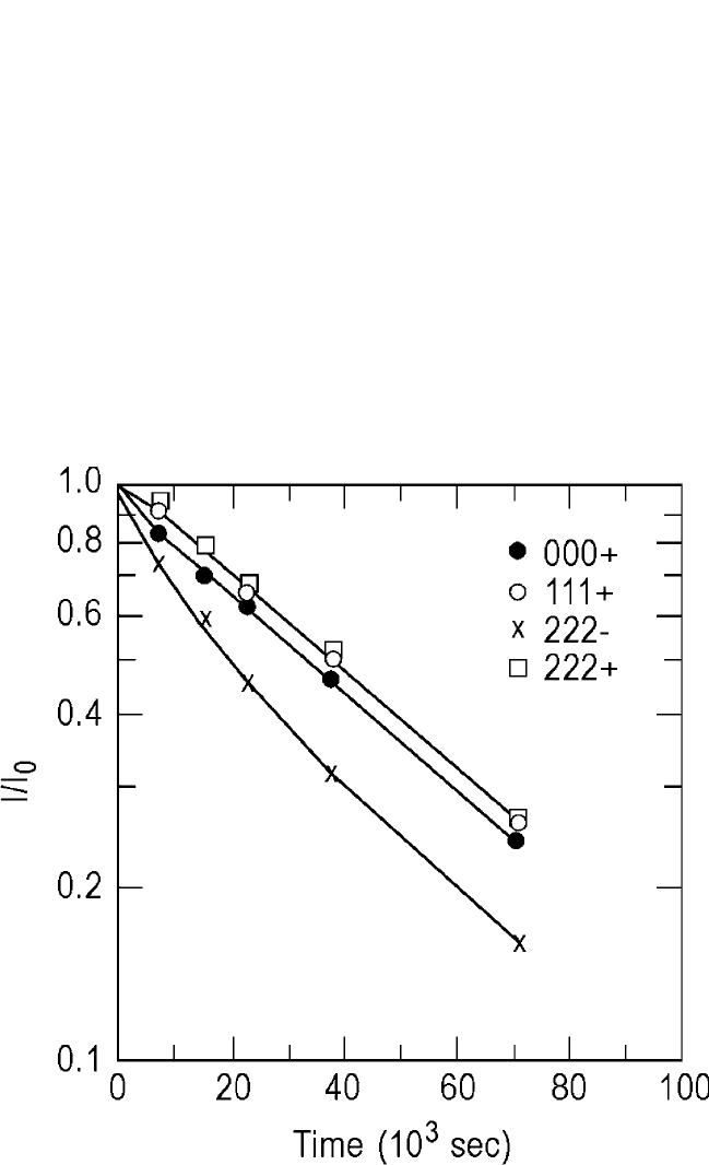
The example of Ag/Au interdiffusion is provided from the investigation
of Cook and Hilliard.
[34]
Figure 1.7 shows x-ray intensities vs. annealing
26 DIFFUSION PROCESSES IN ADVANCED TECHNOLOGICAL MATERIALS
Figure 1.7 Logarithmic plots of the relative x-ray intensity of the satellite peaks
(log II
o
) vs. annealing time at 228.3°C in an Ag-Au modulated thin-film package
of 3.35-nm wavelength with an average composition of 32 at.% Au. (From Cook
and Hilliard
[34]
)
Ch_01.qxd 11/30/04 8:36 AM Page 26

DIFFUSION IN BULK SOLIDS AND THIN FILMS, GUPTA 27
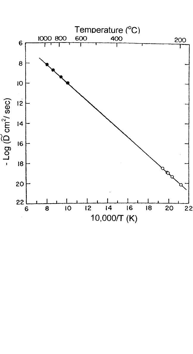
time plots at 228.3°C for 000, 111, 222, and 222 satellite peaks in
Ag-Au modulated films. The diffusion coefficients obtained are shown in
Fig. 1.8; they agree extremely well with the interdiffusivities (D
∼
) measured
by Johnson
[44]
in the Ag
50
Au
50
alloy at high temperatures using chemical ana-
lytical techniques over 12 orders of magnitude. Even more remarkable is the
fact that a diffusion coefficient as low as 10
24
m
2
s
1
involving only one or
two atomic jumps could be measured in a short period of a few hours!
1.3 Structurally Inhomogeneous Samples
The discussions in Sections 1.1 and 1.2 assumed that the diffusion
samples were structurally homogeneous, that is, free from such extended
Figure 1.8 Arrhenius plot of the interdiffusion coefficients (D
∼
) in the Ag
50
Au
50
mod-
ulated thin-film package (from Cook and Hilliard
[34]
) compared with the high-
temperature data of Johnson
[44]
obtained in a bulk diffusion couple.
Ch_01.qxd 11/30/04 8:36 AM Page 27

defects as dislocations, grain boundaries (GBs), and interfaces.
Consequently, diffusion occurred only in the lattice due to equilibrium
point defects such as vacancies, interstitial atoms, and divacancies.
Engineering materials, however, are polycrystalline in nature and contain
non-equilibrium extended defects. Sutton and Balluffi provide a compre-
hensive treatment of the nature of grain boundaries and their kinetic
behavior.
[45]
Diffusion along these defects is commonly six or more orders
of magnitude more rapid than in monocrystalline samples. In thin-film
packages used in the ultra-large-scale integration (ULSI) of microelec-
tronic devices, the density of the structural defects, notably the GBs, is
very high. Because the temperatures of device fabrication and perform-
ance are low, ≈100°C, the diffusive process in thin films may be largely
controlled by the grain boundaries. In recent years, interfaces in the
microelectronic back-end metallization/dielectric packages have also
been considered paths for fast diffusion (see, for example, Chapter 9).
Because an interface is sandwiched between two materials, it may be
termed a heterogeneous boundary as opposed to the homogeneous grain
boundary, which consists of the same material on either side. We use the
interface and grain boundary terms interchangeably because their analyt-
ical treatment is almost identical, with only a small adjustment to account
for lattice diffusion in differing materials in the case of the former.
In polycrystalline materials, in general, the diffusion within the
grains and along GBs occurs simultaneously. The coupling of these
processes takes place at the GBs, which have an effective thickness d, of
the order of atomic width ∼0.5 nm. The extent to which the lattice atoms
make excursions into the GBs, or vice versa, determines the diffusion
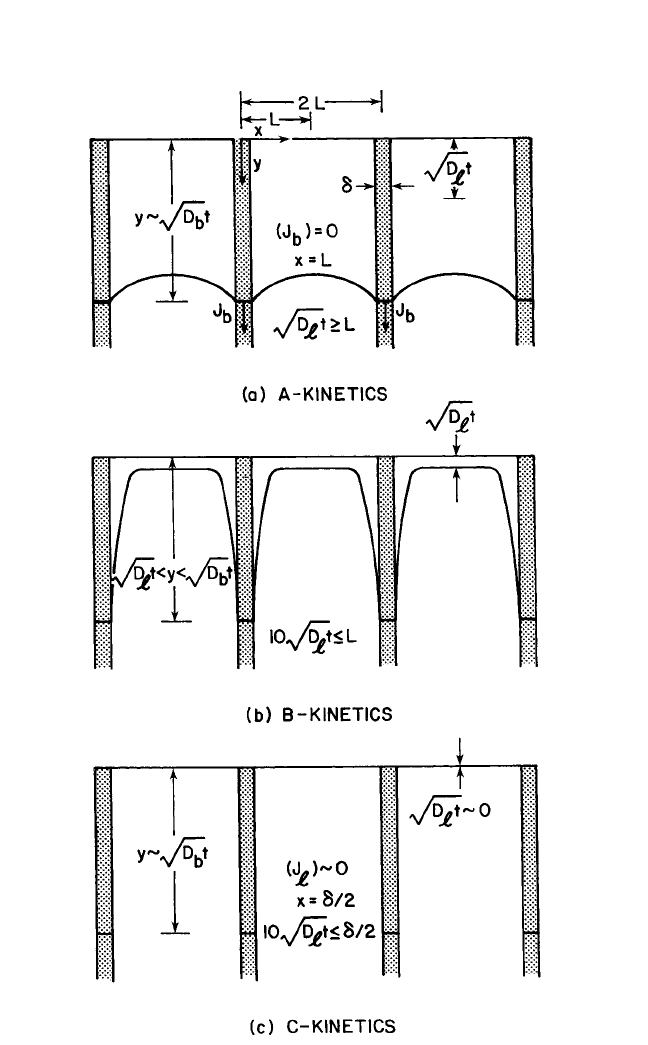
kinetic regime that prevails in the sample as a whole. Harrison
[46]
desig-
nated three types of kinetic regimes known as A, B, and C, which are
shown in Fig. 1.9.
The distinguishing feature of type-A kinetics is the extensive lattice
diffusion, which causes the diffusion fields from the adjoining grains to
overlap. The boundaries are shown here as parallel slabs with spacing 2L.
In essence, the atoms in the lattice have made some excursions into the
GBs so that their transport has been accelerated. The measurements in
type-A kinetics would show enhanced apparent diffusivities (D
app
) with
lower activation energies, which can be described by Hart’s equation:
[47]
D
app
D
1
gD
b
, (60)
where the l and b refer to the lattice and GB, respectively, and g is the site
occupancy factor at the GBs so that g 4dL. The value of g in bulk
materials is ∼10
5
, but in thin films, values of 10
2
are not uncommon.
Consequently, the second term becomes dominant in thin films.
28 DIFFUSION PROCESSES IN ADVANCED TECHNOLOGICAL MATERIALS
Ch_01.qxd 11/30/04 8:36 AM Page 28

DIFFUSION IN BULK SOLIDS AND THIN FILMS, GUPTA 29
Figure 1.9 Schematic representation of Harrison’s A, B, and C kinetic regimes of
grain boundary diffusion.
[46]
The diffusion source coincides with the top horizontal
lines.The three regimes are temperature-sensitive.
Ch_01.qxd 11/30/04 8:36 AM Page 29

In type-B kinetics, the grain boundaries are assumed to be isolated,
and the flux at large distance in the x direction approaches zero.
Effectively, the GB and lattice fields are confined individually to them-
selves. The leakage of mass from the grain boundaries is only in the x
direction, and the contribution of the GBs to the diffusion within the
grains [at the top of Fig. 1.9(b)] is generally neglected in the analysis.
Type-B kinetics is commonly exploited in systematic experimental work,
which is discussed in Sec. 1.4.
In type-C kinetics, lattice diffusion is considered negligible, and sig-
nificant atomic transport occurs only within the boundaries. Atkinson
and Taylor,
[48]
Hwang and Balluffi,
[49]
and, more recently, Surholt et al.
[50]
have carried out type-C diffusion experiments. Type-C kinetics should
be of great significance for the mass transport in thin films at low
temperatures.
Therefore, the mathematical analyses for GB diffusion will differ
from situation to situation, depending on the thickness of the sample, its
grain size, and the relative contribution of the lattice diffusion as dictated
by the temperature of annealing. The mathematical solutions for GB dif-
fusion have been previously reviewed in detail.
[51]
Here, we only discuss
some salient solutions that have commonly been used to evaluate experi-
mental data and that have yielded reliable diffusion coefficients.
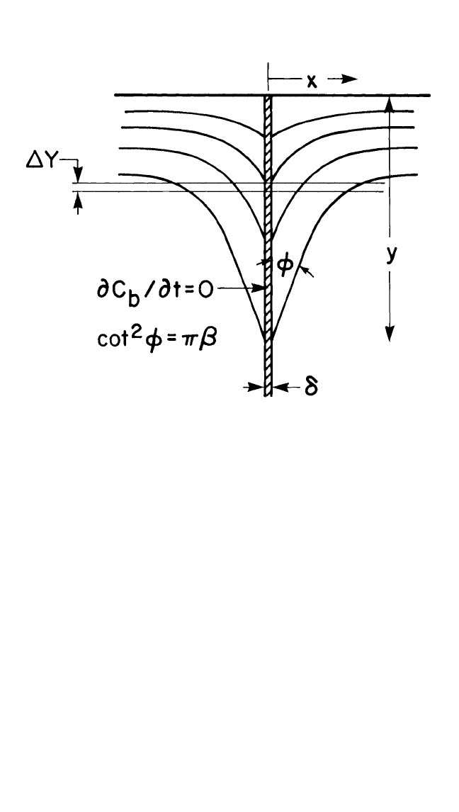
Fisher,
[52]
for the first time, analyzed the coupled lattice and GB diffu-
sion problem for a simple slab configuration in the type-B kinetic regime
shown in Fig. 1.10. The crucial approximation in the Fisher solution was
that the concentration C
b
within the boundary changed so slowly with time
t that the term ∂C
b
∂t could be set equal to zero. Subsequently, Whipple
[53]
and Suzuoka
[54]
have solved the problem exactly, removing this limitation.
In discussing the solutions, it is more convenient to use reduced vari-
ables defined as follows:
h
y
D
l
t
, x
x
(
D
d
l
t
2)
, a
2
d
D
l
t
, ∆
D
D
b
l
, and b (∆ 1)a.
(61)
The Fisher solution for the slab geometry may be written as:
dD
b
0.56
∂ l
∂
n
y
C
2
4D
t
l
12
, (62)
with the condition that ∂C
b
∂t 0 in the slab, where C
is the concentra-
tion of the diffusant in the sectioning method of determining the diffusivities.
30 DIFFUSION PROCESSES IN ADVANCED TECHNOLOGICAL MATERIALS
Ch_01.qxd 11/30/04 8:36 AM Page 30

DIFFUSION IN BULK SOLIDS AND THIN FILMS, GUPTA 31
The Fisher solution is written in this form for easy comparison with the
Whipple and Suzuoka solutions.
The solution for the slab geometry of the GB, according to Whipple
[53]
and Suzuoka,
[54]
is given by:
dD
b
∂
∂
l
y
n
6
C
5
53
4D
t
l
12
[∂(h
∂
b
l
)
n
C
1
2
]
65
53
. (63)
For large values of b 30, the third term converges to (0.78)
53
and
(0.72b
.008
)
53
for infinite and instantaneous source conditions, respectively.
Consequently, the asymptotic Whipple and Suzuoka solutions can be
approximated as:
dD
b
0.661
∂
∂
l
y
n
6
C
5
5 3
4D
t
l
12
. (64)
Figure 1.10 Grain boundary diffusion measurements by sectioning methods: Is
concentration contours are averaged in a section of thickness ∆Y. The profile is
analyzed according to Eqs. (63) and (64) where the angle φ is well-defined.
Ch_01.qxd 11/30/04 8:36 AM Page 31
