Endo M., Iijima S., Dresselhaus M.S. (eds.) Carbon nanotubes
Подождите немного. Документ загружается.


11s
X.
K.
WANG
et
al.
Fig.
9.
Photographs of the cross-section of the deposited rods; photos (a) and (b) were taken from deposited
rods produced by the glow discharge and by the conventional arc discharge, respectively.
note that the average diameter of the bundles decreases
towards the perimeter of the deposited rod. The clad-
ding shell around the rod is composed of fused gra-
phitic flakes. The geometry and the distribution of the
bundles in the deposited rod may be interpreted as fol-
lows. In the glow mode, the highest temperature occurs
Fig.
10.
A
SEM
micrograph of the cross-section
of
the
deposited rod synthesized by the glow discharge shows an im-
age of
1/4
of the cross-section of the deposited rod; upper
left corner of the image corresponds to the center of the end
of the deposited rod.
at the center of the deposited rod and the temperature
decreases towards the perimeter because the heat is
transported by both radiation and conduction via the
He gas. In the cladding shell area, the temperature
may not be high enough to form the bundles but is
sufficient to form fused graphitic materials. Although
several groups have speculated on the effect of the
electric field in the formation of buckytubes[
13-
16,471,
the influence of the temperature on the yield
and distribution of the bundles has not been discussed.
From
our
results, we may conclude that the tempera-
ture is one of the key factors in the formation
of
buckybundles.
Figure
11
shows two typical TEM images for the
deposited rods synthesized in the glow mode and the
conventional arc mode, respectively. Two samples for
TEM observation were prepared in an identical way.
The figures show the dramatic improvement in the
yield and quality of buckytubes synthesized in the glow
mode. The buckytubes and their bundles shown in
Fig.
11
(a) are thicker and longer than that shown in
Fig.
11
(b). The length of the tubes shown here is
larger than the field of view of HREM used in this
study.
Our
systematic studies indicated that the yield
of the tubes made by the glow discharge is at least
20
times larger than that of the tubes made by the arc dis-
charge. In the arc mode, the jumping of the arc causes
an instability of the electric field which leads to a clo-
sure of the tube tips,
so
as to minimize dangling bonds
and lower the total energy. Therefore, the conven-
tional arc discharge produces a low yield of low-
quality buckytubes.
Note also that a large number of the tube tips,
shown in Fig.
11
(b), are closed by caps that are po-
lygonal or cone-shaped. Iijima has found that the

Properties of buckytubes and derivatives
119
Fig.
11.
(a) and (b) are
HREM
images
of
the deposited rods produced by the glow discharge and by the
conventional arc discharge, respectively.
polygonal and cone-shaped caps are formed by incor-
porating pentagons into the hexagonal network. He
speculated that the formation of the pentagons may
result from
a
depletion of carbon in plasma near the
end of cathode[2]. Our experimental results offer ev-
idence for the above speculation. Fluctuations of car-
bon species caused by
a
discontinuous arc discharge
may be responsible for the formation of short tubes
with the caps, consisting of pentagons and other
defects.
Based on these experimental results, one can spec-
ulate on the influence of the arc mode on the yield and
distribution of the bundles. For the glow discharge,
the plasma is continuous, homogeneous, and stable.
In other words, the temperature distribution, the elec-
tric field which keeps growing tube tips open[47], and
the availability of carbon species (atoms, ions, and
radicals) are continuous, homogeneous, and stable
over the entire central region of the cathode. Accord-
ingly, a high yield and better quality buckytubes
should occur over the entire central region of the cath-
ode. These are consistent with what we observed in
Fig.
9
(a), Fig.
10,
and Fig.
11
(a). For the conven-
tional arc discharge, we can speculate that the arc
starts at
a
sharp edge near the point of closest ap-
proach, and after vaporizing this region it jumps to
what then becomes the next point of closest approach
(usually within about
a
radius of the arc area), and
so
on. The arc wanders around on the surface of the end
of the anode, leading, on the average, to
a
discontin-
uous
evaporation process and an instability of the elec-
tric field. This kind of violent, randomly jumping arc
discharge is responsible for the low yield and the low
quality of the deposited buckytubes. This is, again,
consistent with what we showed in Fig. 9(b) and
Fig.
11
(b). Note also from Fig.
11
that carbon nano-
tubes and nanoparticles coexist in both samples. The
coexistence of these two carbonaceous products may
suggest that some formation conditions, such as the
temperature and the density of the various carbon spe-
cies, are almost the same for the nanotubes and the
nanoparticles. An effort to promote the growth of car-
bon nanotubes and eliminate the formation of carbon
nanoparticles is presently underway.
4.
CONCLUSIONS
In this article, we have reported the structural,
magnetic, and transport properties of bundles of
buckytubes produced by an arc discharge. By adjust-
ing the arc mode into
a
stable glow discharge, evenly
spaced and parallel buckybundles with diameters up to
200
pm have been synthesized. The magnetic suscep-
tibility of
a
bulk sample of buckybundles is
-10.75
x
emu/g for the magnetic field parallel to the bun-
dle axes, which is approximately
1.1
times the perpen-
dicular value and 30 times larger than that of
c60.
The magnetoresistance (MR) and Hall coefficient mea-
surements on the buckybundles show
a
negative MR
at low temperature,
a
positive MR at a temperature
above
60K,
and a conductivity which increases ap-
proximately linearly with temperature.
Our
results
show that a buckybundle may best be described as a
semimetal.
Acknowledgements-We are grateful to A. Patashinski for
useful discussions. This work was performed under the sup-
port of
NSF
grant
#9320520
and
DMR-9357513
(NYI award
for
VPD).
The use of
MRC
central facilities supported by
NSF is gratefully acknowledged.
REFERENCES
1.
S.
Iijima, Nature
354,
56 (1993).
2.
S.
Iijima, T. Ichihashi, and Y. Ando, Nature
356,
776
(
1992).
3.
T. W. Ebbesen and
P. M.
Ajayan, Nature
358,
220
(1992).
4.
Y.
Ando and
S.
Iijima,
Jpn.
J.
Appl.
Phys.
32,
L107
(1993).
5.
T. W. Ebbesen, H. Hiura,
J.
Fujita, Y. Ochiai,
S.
Mat-
sui, and
K.
Tanigaki,
Chem.
Phys. Lett.
209,
83 (1993).
6.
Y.
Saito, T. Yoshikawa,
M.
Inagaki,
M.
Tomita, and
T.
Nayashi, Chem. Phys. Lett.
204,
277 (1993).

120
X.
K. WANG
et ai.
7.
Z. Zhang and
C.
M. Lieber,
Appl. Phys. Lett.
62,2792
8.
S.
N.
Song,
X.
K. Wang, R.
P.
H. Chang, and
J.
B. Ket-
9.
D. Ugarte,
Nature
359, 707 (1992).
(1993).
terson,
Phys. Rev. Lett.
72, 697 (1994).
10. S.
Iijima,
P.
M.
Ajayan, and
T.
Ichihashi,
Phys. Rev.
Lett.
69, 3100 (1992).
11.
R. A. Jishi,
M.
S.
Dresselhaus, and G. Dresselhaus,
Phys. Rev.
B
48,
11385 (1993).
12.
L. Langer, L. Stockman,
J.
P.
Heremans,
V.
Bayot,
C.
H.
Olk,
C.
V.
Haesendonck, and Y. Bruynseraede,
J.
Mater. Res.
9, 927 (1994).
13.
J.
W. Mintmire, B.
I.
Dunlap, and C.
T.
White,
Phys.
Rev. Lett.
68, 631 (1992).
14.
D. H. Robertson,
D.
W. Brenner, and
J.
W. Mintmire,
Phys. Rev.
B
45, 12592 (1992).
15.
N. Hamada,
S.
I.
Sawana, and A. Oshiyama,
Phys. Rev.
Lett.
68, 1579 (1993).
16.
R. Saito,
M.
Fujita,
G.
Dresselhaus, and M.
S.
Dressel-
haus,
Mater. Res.
SOC.
Symp. Proc.
247, 333 (1992).
17.
G.
Dresselhaus,
M.
S.
Dresselhaus, and R. Saito,
Phys.
Rev.
B45, 6234 (1992).
18.
H. W. Kroto,
J.
R.
Heath,
S.
C. O’Brien, R.
E
Curl, and
R.
E.
Smalley,
Nature
318, 162 (1985).
19.
R. Tycko, R.
C.
Haddon,
G.
Dabbagh,
S.
H. Glarum,
D. C. Douglass, and
A.
M. Mujsce,
J.
Phys. Chem.
95,
518 (1991).
20. S.
Iijima and T. Ichihashi,
Nature
363, 603 (1993).
21.
D.
S.
Bethune, C.
H.
Klang,
M.
S.
deVries, G. Gorman,
R. Savoy,
J.
Vazqiez, and R. Beyers,
Nature
363, 605
(1993).
22.
X.
W. Lin,
X.
K. Wang,
V.
P.
Dravid,
R.
P.
H. Chang,
and
J.
B. Ketterson,
Appl.
Phys. Lett.
64, 181 (1994).
23.
R. E. Haufler, J. Conceicao,
L.
P.
E
Chibante, Y. Chai,
N.
E. Byme,
S.
Flanagan, M. M. Haley, S. C. O’Brien,
C. Pan,
Z.
Xiao, W.
E.
Billups,
M.
A.
Ciufolini, R. H.
Hauge,
J.
L. Margrave, L.
J.
Wilson, R.
F.
Curl, and
R.
E.
Smalley,
J.
Phys. Chem.
94, 8634 (1990).
24.
V.
Elser and
R.
C. Haddon,
Nature
325, 793 (1987).
25.
R. C. Haddon, L. F. Schneemeyer,
J.
V. Waszczak,
S.
H.
Glarum,
R.
Tycko,
G.
Dabbagh, A.
R.
Kortan,
A.
J.
Muller,
A.
M.
Mujsce, M.
J.
Rosseinsky,
S.
M.
Za-
hurak,
A.
V.
Makhija,
F.
A.
Thiel, K. Raghavachari,
E.
Cockayne, and
V.
Elser,
Nature
350,
46 (1991).
26.
A. Pasquarello, M. Schluter, and R.
C.
Haddon,
Science
27.
P.
W. Fowler,
P.
Lazzeretti, M. Malagoli, and R. Zanasi,
28.
T.
G.
Schmalz,
Chem. Phys. Lett.
175,
3
(1990).
29.
R.
S.
Ruoff,
D. Beach,
J.
Cuomo,
T.
McGuire, R.
L.
Whetten, and
E.
Diederich,
J.
Phys. Chem.
95,
3457
(1
991).
30.
H.
Ajiki and
T.
Ando,
J.
Phys.
SOC.
Japan
62, 2470
1993.
31.
V.
P.
Dravid,
X.
W. Lin, Y. Y. Wang,
X.
K. Wang,
A.
Yee,
J.
B.
Ketterson, and H.
P.
H.
Chang,
Science259,
1601 (1993).
32.
X.
K. Wang,
X.
W. Lin,
V.
P.
Dravid,
J.
B. Ketterson,
and
R.
P.
H.
Chang,
Appl. Phys. Lett.
62, 1881 (1993).
33.
J.
C.
Slonczewski and
P.
R. Weiss,
Phys. Rev.
109,
272
(1958).
34.
J.
W. McClure,
Phys. Rev.
199,
606 (1960).
35.
R. M. White,
Quantum Theory
of
Magnetism, Springer
Series in Solid State Sciences,
Springer-Verlag Berlin,
Heidelberg, New York
(1983).
36.
X.
K.
Wang, R.
P.
H. Chang,
A.
Patashinski, and
J.
E.
Ketterson,
J.
Mater. Res.
9,
1578 (1994).
37. S.
Saito and
A.
Oshiyama,
Phys. Rev. Lett.
66, 2637
(1
99 1).
38.
L.
Pauling,
J.
Chem. Phys.
4,
637 (1936).
39.
S.
N. Song,
X.
K. Wang, R.
P.
H.
Chang, and
J.
B. Ket-
40.
J.
Callaqay,
In
Quantum Theory
of
the
Solids,
p.
614,
41.
P.
Delhaes,
P.
de Kepper, and
M.
Uhlrich,
Philos. Mag.
42.
M.
Ge and
K.
Sattler,
Appl. Phys. Lett.
64, 710 (1994).
43.
M.
J.
Yacaman,
M.
M. Yoshida,
L.
Rendon, and
J.
G.
Santiesteban,
Appf.
Phys. Lett.
62, 657 (1993).
44.
M. Endo and H. W. Kroto,
J.
Phys. Chem.
96,
6941
(1992).
45.
J.
R.
Brock and
P.
Lim,
Appl. Phys. Lett.
58, 1259
(1991).
46.
0.
Zhou,
R.
M. Fleming,
0.
W.
Murphy, C. H. Chen,
R. C. Haddon,
A.
P.
Ramire, and
S.
H.
Glarum,
Sci-
ence
263, 1774 (1994).
257, 1660 (1992).
Chem. Phys. Left.
179, 174 (1991).
terson,
Phys. Rev. Lett.
72, 679 (1994).
Academic Press, New York
(1976).
29, 1301 (1974).
47.
R.
E.
Smalley,
Mater. Sci.
Engin.
B19,
1
(1993).

ELECTRONIC PROPERTIES
OF
CARBON NANOTUBES:
EXPERIMENTAL RESULTS
J.-P.
ISSI,’
L.
LANGER,’
J.
HEREMANS?
and
C.
H.
QLK~
‘Unite PCPM, Universitt Catholique de Louvain, Louvain-la-Neuve, Belgium
2General Motors Research and Development Center, Warren,
MI
48090, U.S.A.
(Received
6
February
1995,
accepted
10
February
1995)
Abstract-Band structure calculations show that carbon nanotubes exist as either metals or semiconduc-
tors, depending
on
diameter and degree
of
helicity. When the diameters of the nanotubes become com-
parable to the electron wavelength, the band structure becomes noticeably one-dimensional. Scanning
tunneling microscopy and spectroscopy data
on nanotubes with outer diameters from
2
to
10
nm show
evidence of onedimensional behavior: the current-voltage characteristics
are
consistent with the functional
energy dependence
of
the density-of-states in
1D
systems. The measured energy gap values vary linearly
with the inverse nanotube diameter. Electrical resistivity and magnetoresistance measurements have been
reported
for
larger bundles, and the temperature dependence of the electrical resistance
of
z
single micro-
bundle was found
to
be similar to that of graphite and
its
magnetoresistance was consistent with the for-
mation
of
Landau levels. Magnetic susceptibility data taken
on
bundles
of
similar tubes reveal
a
mostly
diamagnetic behavior. The susceptibility at fields above the value at which
the
magnetic length equals the
tube diameter has a graphite-like dependence
on
temperature and field. At
low
fields, where electrons
sari.-
ple the effect
of
the Finite tube diameter, the susceptibility has a much more pronounced temperature
dependence.
Key
W70rds--Carbon nanotubes, scanning tunneling microscopy, spectroscopy, magnetoresistance, elec-
trical resistivity, magnetic susceptibility.
1.
INTRODUCTION
The existence of carbon nanotubes with diameters
small compared
to
the de Broglie wavelength has been
described by Iijima[l,2,3] and others[4,5]. The energy
band structures for carbon nanotubes have been cal-
culated by
a
number
of
authors and the results are
summarized in this issue by
M.S.
Dresselhaus,
6.
Dres-
selhaus, and
R.
Saito. In short, the tubules can be
either metallic or semiconducting, depending
on
the
tubule diameter and chirality[6,7,8]. The calculated
density
of
states[8] shows
I/(KEj)’’’
singularities
characteristic of one-dimensional
(1D)
systems. The
separation between the singularities around the Fermi
energy is the energy gap for the tubes that are semi-
conducting, and scales linearly with the inverse of the
tube outer diameter[7,8]. This contrasts with the case
of
a
rod-shaped quantum wire, for which the gap is
expected
to
scale with the inverse square
of
the diam-
eter. The relevant energy scale for the gap in carbon
nanotubes
is
the nearest-neighbor overlap integral
in
graphite (3.14 eV)[9]. This makes room-temperature
observation of the quantum size effects, in principle,
possible in nanotubes with diameters in the
nm
range,
because the sublevel energy separations are of the or-
der
of
1
eV.
Experimental measurements
to
test these remark-
able theoretical predictions of the electronic structure
of
carbon nanotubes are difficult
to
carry out because
of
the strong dependence of the predicted properties
on
tubule diameter and chirality. Ideally, electronic or
optical measurements should be made on individual
single-wall nanotubes that have been characterized
with regard
to
diameter and chiral angle. Further ex-
perimental challenges result from the fact that tubes
are often produced in bundles,
so
that obtaining data
on
single, well-characterized tubes has
not
yet been
achieved. We review here some experimental observa-
tions relevant
to
the electronic structure
of
individ-
ual nanotubes or
on
bundles
of
nanotubes: combined
scanning tunneling microscopy and spectroscopy,
temperature-dependent resistivity, magnetoresistance
(MR),
and magnetic susceptibility.
2.
SCANNING TUNNELING
SPECTROSCOPY STUDIES
Scanning tunneling spectroscopy (STS) can,
in
prin-
ciple, probe the electronic density of states
of
a single-
wall
nanotube, or the outermost cylinder
of
a multi-wall
tubule, or of a bundle of tubules. With this technique,
it is further possible to carry
out
both
STS
and scan-
ning tunneling microscopy
(STM)
measurements at the
same location
on
the same tubule and, therefore,
to
measure the tubule diameter concurrently with the
STS
spectrum.
No
reports have yet been made of a deter-
mination of the chiral angle of a tubule with the
STM
technique. Several groups have, thus far, attempted
STS
studies
of
individual tubules.
The first report
of
current-voltage (I-V) measure-
ments by Zhang and Lieber[lO] suggested a gap in the
density of states below about 200 MeV and semicon-
ducting behavior in the smallest
of
their nanotubes
(6
nm diameter). The study that provides the most de-
tailed test
of
the theory for the electronic properties
of the 1D carbon nanotubes, thus far, is the combined
STM/STS study by
Olk
and
Heremans[
111,
even though
it is still preliminary. In this study, more than nine
121

122
J.-P.
ISSI
et
ul.
Fig.
1.
Topographic
STM
scan of a bundle of nanotubes. STS data were collected at points
(I),
(2),
and
(3),
on tubes with diameters of
8.7,
4.0,
and
1.7
nm, respectively. The diameters were determined from
image cross-sections of the variations in height in a direction perpendicular to the tubes (adapted from
Olk
et
u/.[ll]).
individual multilayer tubules with diameters ranging
from
2
to
10
nm, prepared by the standard carbon-arc
technique, were examined.
STM
measurements were
taken first, and a topographic STM scan of a bundle
of nanotubes is shown in Fig. 1. The exponential re-
lation between the tunneling current and the tip-to-
tubule distance was experimentally verified to confirm
that the tunneling measurements pertain to the tubule
and not to contamination on the tubule surface. From
these relations, barrier heights were measured to estab-
lish the range in which the current-voltage character-
istics can be taken for further
STS
studies. The image
in Fig.
1 is used to determine the diameter of the in-
dividual tubule on which the STS scans are carried
out. During brief interruptions in the STM scans, the
instrument was rapidly switched to the STS mode of
operation, and I-V plots were made on the same re-
gion
of
the same tubule as was characterized for its di-
ameter by the STM measurement. The I-V plots for
three typical tubules, identified
(1)-(3),
are shown in
Fig. 2. The regions (1)-(3) correspond to interruptions
in the STM scans at the locations identified by crosses
in the topographic scan, Fig. 1. Although acquisition
of spectroscopic data in air can be complicated by
contamination-mediated effects on the tunneling gap,
several studies on
a
wide variety of surfaces have been
reported[l2]. Trace (1) in Fig.
2,
taken on a tube with
8.7
nm diameter, has an ohmic behavior, providing ev-
idence for the metallic nature of that tubule. Two tu-
bules (trace
2
for a tubule with diameter
=
4.0
nm, and
trace
3
for a tubule with diameter
=
1.7
nm)
show pla-
teaus in the I/V characteristics at zero current. This
rectifying behavior is the signature of semiconducting
tubules. The dI/dV plot in the inset crudely mimics a
1D density
of
states, the peaks in the dI/dV plot be-
Fig.
2.
Current-voltage characteristics taken at points
(l),
(2),
and
(3)
in Fig.
3.
The top insert shows the conductance versus
voltage plot, for the data taken at point
(3)
(adapted from
Olk
et
ul.[ll]).

Electronic properties
ing attributed
to
[I/(&,
-
E)’”] -type singularities in
the
1D
density of states seen in the density of states
versus energy diagrams calculated in[8]. Several
I-V
curves were collected along the length of each tube.
Reproducible spectra were obtained on
9
tubes with
different diameters.
The energy gap of the semiconducting tubes was es-
timated around
V
=
0
V
by drawing two tangents at the
points of maximum slope nearest zero in the
I-V
spec-
tra, and measuring the voltage difference between the
intercepts
of
these tangents with the abscissa. A plot of
these energy gaps versus inverse tube diameter for
all
samples studied is shown in Fig. 3[11]. Surface contam-
ination may account for the scatter in the data points,
though the correlation between
Eg
and the inverse di-
ameter shown in Fig. 3 is illustrated by the dashed line.
The data in Fig. 3 is consistent with the predicted de-
pendence on the inverse diameter[ 131. The experimen-
tally measured values of the bandgaps are, however,
about
a
factor
of
two greater than the theoretically
estimated ones
on
the basis of a tight binding calcu-
lation (full line in Fig. 3)[7,13]. Further experimental
and theoretical work is needed to reach
a
detailed un-
derstanding of these phenomena.
3. ELECTRICAL RESISTIVITY AND
MAGNETORESISTANCE
The remarkable theoretical predictions mentioned
above are even more difficult to verify by experimen-
tal measurements
in
the case of electrical conductivity.
Ideally, one has to solve two experimental problems.
First, one has
to
realize a four-point measurement on
an individual nanotube. That means four contacts
on
a
sample with typical dimensions
of
the order
of
a
nm
1.6
1.2
n
3
-0.8
Fig. 3. Energy gap versus inverse nanotube diameter,
for
the
nine nanotubes studied; the dashed line
is
a
regression
through the points, the
full
line is
a
calculation
for
semicon-
ducting
zigzag nanotubes[7,13] (adapted
from
Olk
et
aL[ll]).
of
carbon nanotubes
123
diameter and a few pm length. Second, this sample
with its contacts must be characterized to determine
its exact diameter and helicity. To take up this chal-
lenge it is necessary to resort to nanotechnologies.
Before reviewing the results of different measure-
ments, we need to first briefly describe the nature of
the deposit formed during the carbon-arc experiment
in a way first proposed by EbbesentS]. He suggested
that the carbon nanotubes produced by classical car-
bon arc-discharge present
a
fractal-like organization.
The deposit
on
the negative electrode consists of
a
hard gray outer shell and
a
soft black fibrous core con-
taining the carbon nanotubes. If we examine in detail
this core material by scanning electron microscopy, we
observe a fractal-like structure. This means that the
black core is made of fiber-like entities that are, in re-
ality, bundles of smaller fiber-like systems. These
smaller systems are, in turn, formed of smaller bundles,
and
so
on.
The micro-bundle, which is the smallest
bundle, consists of a few perfectly aligned nanotubes
of
almost equal lengths. Finally, each of these individ-
ual nanotubes is generally formed of several concen-
tric single-shell nanotubes.
The fractal-like organization led, therefore, to con-
ductivity measurements at three different scales:
(1)
the macroscopic, mm-size core
of
nanotube contain-
ing material,
(2)
a large
(60
pm) bundle
of
nanotubes
and, (3) a single microbundle,
50
nm in diameter.
These measurements, though they do not allow direct
insights on the electronic properties
of
an individuai
tube give, nevertheless, at a different scale and within
certain limits fairly useful information
on
these
properties.
Ebbesen[4] was the first to estimate
a
conductiv-
ity
of
the order of Qm for the black core bulk
material existing in two thirds
of
tubes and one third
of nanoparticles. From this observation, it may
nat-
urally be inferred that the carbon arc deposit must
contain material that is electricaliy conducting. An
analysis
of
the temperature dependence of the zero-
field resistivity of similar bulk materials[ 14,151 indi-
cated that the absolute values of the conductivity were
very sample dependent.
Song
et
al.
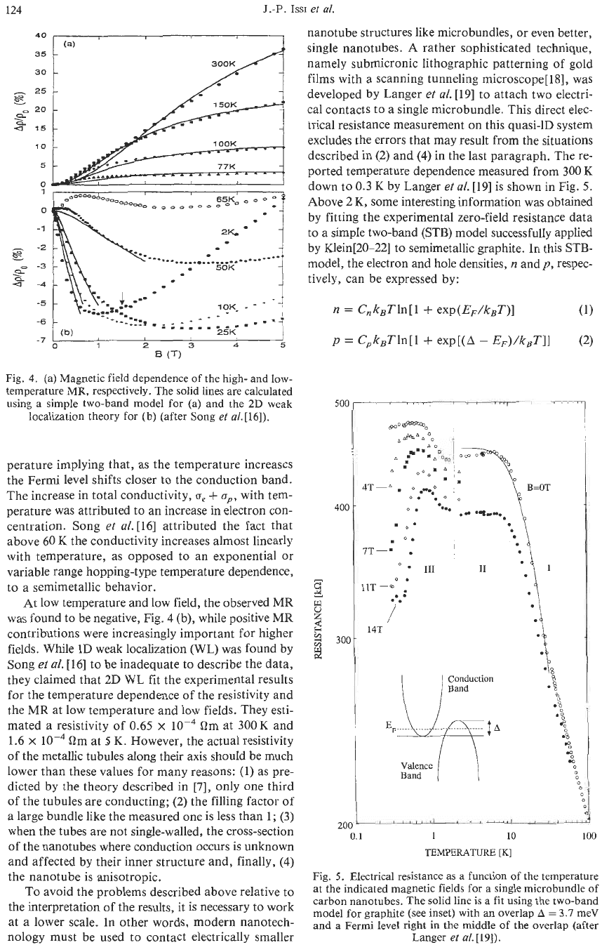
[16] reported results relative to a four-
point resistivity measurement on a large bundle of car-
bon nanotubes (60 pm diameter and 350 pm in length
between the two potential contacts). They explained
their resistivity, magnetoresistance, and
Hall
effect re-
sults in terms of
a
conductor that could be modeled
as
a
semimetal. Figures
4
(a) and (b) show the mag-
netic field dependence they observed
on
the high- and
low-temperature
MR,
respectively.
At high temperature, the conductivity was found
to increase linearly with temperature and the observed
high-temperature
MR
was positive.
In
fact, by fitting
the data using a simple two-band model[l7] the au-
thors obtained the theoretical curve
in
Fig.
4
(a). The
fitting parameters showed that the ratio
u,/a,,
where
up
and
a,
are the partial conductivities
of
holes and
electrons, respectively, decreases with increasing tem-
124
J.-P.
ISSI
et
al.
Fig.
4.
(a) Magnetic
field
dependence of
the
high- and low-
temperature
MR,
respectively. The solid
lines
are calculated
using
a simple two-band model for (a) and the
2D
weak
localization theory for
(b)
(after
Song
et
a/.[16]).
perature implying that, as the temperature increases
the Fermi level shifts closer to the conduction band.
The increase in total conductivity,
a,
+
up,
with tem-
perature was attributed to an increase in electron con-
centration. Song
et
al.
[16]
attributed the fact that
above
60
K
the conductivity increases almost linearly
with temperature, as opposed
to
an exponential or
variable range hopping-type temperature dependence,
to
a semimetallic behavior.
At low temperature and low field, the observed MR
was found to be negative, Fig.
4
(b), while positive MR
contributions were increasingly important for higher
fields. While
1D
weak localization
(WL)
was found by
Song
et
al.
[lq
to be inadequate
to
describe the data,
they claimed that 2D WL fit the experimental results
for the temperature dependence of the resistivity and
the MR at low temperature and low fields. They esti-
mated
a
resistivity
of
0.65
x
lop4
Qm
at
300
K
and
1.6
x
Om
at
5
K.
However, the actual resistivity
of
the metallic tubules
along
their
axis
should be much
lower than these values for many reasons:
(1)
as
pre-
dicted by the theory described in
[7],
only one third
of
the tubules are conducting;
(2)
the filling factor of
a
large bundle like the measured one is less than
1;
(3)
when the tubes are not single-walled, the cross-section
of the nanotubes where conduction
occurs
is
unknown
and affected by their inner structure and, finally,
(4)
the nanotube is anisotropic.
To
avoid the problems described above relative to
the interpretation
of
the results, it is necessary to work
at
a
lower scale.
In
other words, modern nanotech-
nology must be used to contact electrically smaller
nanotube structures like microbundles, or even better,
single nanotubes.
A
rather sophisticated technique,
namely submicronic lithographic patterning
of
gold
films with a scanning tunneling microscope[
181,
was
developed by Langer
et
al.
[
191
to
attach two electri-
cal contacts to a single microbundle. This direct elec-
trical resistance measurement
on
this quasi-1D system
excludes the errors that may result from the situations
described in (2) and
(4)
in
the last paragraph. The re-
ported temperature dependence measured from
300
K
down to
0.3
K
by Langer
et
al.
[19]
is shown in Fig.
5.
Above
2
K,
some interesting information was obtained
by fitting the experimental zero-field resistance data
to
a
simple two-band
(STB)
model successfully applied
by Klein[20-22] to semimetallic graphite.
In
this
STB-
model, the electron and hole densities,
n
andp, respec-
tively, can be expressed by:
p
=
C,k,Tln[l
+
exp[(A
-
EF)/kBTII
(2)
500
400
-
8
Y
2
I
,
,,,.11
I
1
I11
I1
'8
0%
I
w

Electronic properties
where
Ef
is the Fermi energy and
A
is the band over-
lap.
C,
and
C,
are the fitting parameters. The results
of this fit, which
is
shown in Fig. 5, is obtained for
A
=
3.7 MeV and with the Fermi energy right in the
middle
of
the overlap. Ideally, an overlap
of
the or-
der of
40
MeV is expected for the case of multilayered
nanotubes[23] with an interlayer configuration simi-
lar to that of crystalline graphite. For real nanotubes
instead, a turbostratic stacking of the adjacent layers
would reduce drastically the interlayer interactions, as
in disordered graphite, and
so
it is not surprising
to
find
a
band overlap
10
times
smaller than in crystalline
graphite. This implies also that, within the frame
of
the STB model, the carrier density is
10
times smaller.
The apparent electrical resistivity
(4
x
Om) mea-
sured at low temperature
is
certainly still higher than
the resistivity of
a
single nanotube. In fact, the con-
ductance of the system is dominated by that
of
the
nanotubes with the highest conductance (Le., the semi-
metallic nanotubes). All these nanotubes are not nec-
essarily in contact with the measuring probes. Finally,
the inner structure of each individual nanotube in this
microbundle remains unknown.
By
applying
a
magnetic field normal to the tube
axis, Langer
et
ai.
I191 observed
a
MR (Fig.
6)
which,
in contrast to the case of graphite, remains negative
at all fields. The negative
MR
was found consistent
with the formation of Landau levels. Ajiki and Ando[24]
have predicted that a magnetic field applied perpen-
dicularly
to
the sample axis should introduce
a
Lan-
dau level at the crossing of the valence and conduction
bands.
It
results
in
an increase of the density
of
states
at the Fermi level and, hence, a reduction of the re-
sistance, which is in agreement with the experimental
data. Moreover, the theory predicts a MR that is tem-
perature independent at low temperature and decreas-
ing when
kBT
becomes larger than the Landau level.
This is also what was experimentally observed.
Thus,
in contrast to what was reported by Song
et
a/.
[16],
-0.35
'
' '
'
I
0
4
8
12
16
MAGNETIC
FIELD
[TI
Fig.
6.
The magnetic field dependence
of
the magnetoresis-
tance at different temperature for the same microbundle
mea-
sured
in
Fig.
5
(after Langer
et
n1.[19]).
of
carbon nanotubes
125
these results are not consistent with WL. In the frame-
work of
WL,
the observed temperature independent
MR below
10
K
and down to
1
K
could only be ex-
plained in the presence
of
large amounts
of
magnetic
impurities,
as
is the case for some pyrocarbons[25].
However, in the present case, the spectrographic anal-
ysis performed by Heremans
et
al.
[26] excludes the
presence of magnetic impurities.
Below 2
K,
an unexpected temperature dependence
of
the resistance and MR is observed.
As
shown in
Fig.
5,
the resistance presents, after
an
initial increase,
a
saturation or
a
broad maximum and
an
unexplained
sharp drop when
a
magnetic field is applied (see Fig.
6).
Further theoretical work is needed to get a better
un-
derstanding of these striking physical observations. Fi-
nally, it is interesting to note that Whitesides and
Weisbecker[27] developed
a
technique
to
estimate the
conductivity
of
single nanotubes by dispersing nano-
tubes onto lithographically defined gold contacts
to
re-
alize a 'nano-wire' circuit. From this 2-point resistance
measurement and, after measuring the diameter of the
single nanotubes by non-contact AFM, they estimated
the room-temperature electrical resistivity along the
nanotube
axis
to be 9.5
x
low5
Qm. This is consistent
with the values obtained for
a
microbundle by Langer
et
a/.
1191.
The most promising way to study the electrical con-
ductivity of a single nanotube
is,
thus, tightly depen-
dent
on
the development or/and the adaptation of
modern nanolithographic techniques. The goal to
achieve is within reach and
a
detailed study
of
the elec-
tronic properties with reference to helicity and diam-
eter will provide instrumental information about these
fascinating materials.
4.
MAGNETIC SUSCEPTIBILITY
The presence of aromatic-like electrons strongly de-
termines the magnetic susceptibility
of
the diverse
forms
of
carbons. The susceptibility of diamond
(-4.9
x
emu/g) is ascribed to diamagnetic con-
tributions from core and valence electrons, and a Van
Vleck paramagnetic term[28]. Graphite has
an
aniso-
tropic diamagnetic susceptibility[29]. The susceptibil-
ity of graphite[29,30] parallel to the planes is about
equal to the free atom susceptibility
of
-5
x
emu/g, but when the magnetic field is aligned paral-
lel to the c-axis, the susceptibility of graphite (-30
X
lop6
emu/g below
loOK)
is due mainly to free elec-
tron contributions and is much larger. The magnetic
susceptibility of
C60
(-3.5
x
emulg) and
C70
(-5.9
x
10-~
emu/g) is small again[31,32], as a result
of
a cancellation between a diamagnetic and a para-
magnetic term.
In the light of these results, it is not surprising that
a
very large anisotropy has been calculated[24] to ex-
ist in the magnetic susceptibility of nanotubes. The
susceptibility with the field parallel to the tube axis is
predicted
to
be as much as 3 orders
of
magnitude
smaller than that with the field perpendicular. Again,

126
J.-P.
ISSI
et
al.
measurements on individual single-wall well-charac-
terized tubes have not been published to date. Exper-
iments usually involve gathering nanotube material
from several growths, to obtain quantities of material
on
the order of tens of mg. A measurement on ori-
ented bundles of tubes[30] at
0.5
T as a function of
temperature gives evidence for anisotropy. Such a
measurement is, however, easily affected by a small
misalignment of the sample. It is, therefore, possible
that the data reported for the case where the field is
parallel to the tube axis are, in fact, dominated by con-
tributions from the perpendicular susceptibility.
A second study [33] on samples that contain a mix-
ture of nanotubes, together with several percent
"buckyonion"-type structures, was carried out at tem-
peratures between 4.5 and 300
K,
and fields between
0
and
5.5
T. The moment Mis plotted as a function
of field in Fig.
7,
for the low-field range, and in Fig.
8
for the high-field range. The field dependence is
clearly non-linear, unlike that of graphite, in which
both the basal plane and the c-axis moments are lin-
ear in field, except for the pronounced de Haas-van
Alphen oscillations at low temperature.
The a.c. susceptibility
(x
=
dM/dH,
where Mis the
moment), measured at
5,0.4,
and 0.04
T,
is shown as
a function of temperature in
Fig.
9.
Three regimes of
magnetic fields are identified in ref. [33]. The high-
field susceptibility (at
5
T) has a temperature depen-
dence similar to that of graphite, but a magnitude
reduced by a factor of
2.
In this regime, the magnetic
radius (hb/eB)"' becomes shorter than the tube diam-
eter. The electronic diamagnetism is then a local probe
of the graphene planes, and its value is expected
to
be
the geometrical average of that of rolled-up graphene.
Because with the field in the basal plane,
x
is much
smaller than along the c-axis, this geometrical average
comes out to be about
+[30].
The low-field susceptibil-
ity (at 0.04
T)
is a better probe of the finite size effects
of the tubes, because the magnetic length is larger than
0.00
m
cn
>
?
E
-0.04
a,
W
4
S
4
-0.08
4.5
0
1000
2000
3000
4000
5000
6000
-0.12
Magnetic Field (Oe)
Fig.
7.
Field dependence of the moment
of
carbon nanotubes
at the temperatures shown at low magnetic fields (after Here-
mans
et
al.[26]).
0.0
-
(r
2
a,
\-0.2
E
"-0.4
CI
c
a
E
-0.6
0
r
-0.8
-1
.o
0
20000
40000
60000
Magnetic Field
(Oe)
Fig.
8.
Field dependence of the moment of carbon nanotubes
at the temperatures shown at high magnetic fields (after Here-
mans
et
al. [26]).
the tube diameter. The sample, however, consists of a
mixture of semiconducting and metallic tubes. The
component of
x
perpendicular to the tube axis domi-
nates the measured susceptibility, and the value is ex-
pected
to
scale with 1/EF[24]. The electrical resistivity
data show that, even in the metallic samples, the en-
ergy gap is
on
the order of a few MeV[19]. At room
temperature
kBT
>
EF
for both metallic and semicon-
ducting samples. Thus, a thermally activated behavior
is expected for the average susceptibility. Furthermore,
carriers may be scattered at a temperature-dependent
rate, for instance by acoustic phonons. These two
mechanisms are consistent with the much more pro-
nounced temperature dependence of the low-field
susceptibility of nanotubes than of graphite. More
quantitative models remain to be developed.
In
the in-
L'
'
"
'
"
'
"
'" '
"
'
"
I
'
"
'
"
'"#
"
'
"
'
"
'4
Fig.
9.
Susceptibility of carbon nanotubes versus tempera-
ture
at
the different fields identified in the figure (after Here-
mans
el
a/. [26]).

Electronic properties of carbon nanotubes
127
termediate field regime (around
0.5
T),
x
is probably
sensitive to the fact that the sample consists
of
a mix-
ture of semiconducting and metallic tubes. Further-
more, the tubes in that mixture have different diameters
and,
thus, go from the low-field to the high-field re-
gime at different fields. Figure 10 shows a summary
of
the a.c. susceptibilities
of
various forms
of
carbon,
as
an
easy ready reference. The values for diamond
and the basal plane
of
graphite represent the atomic
contributions, and the c-axis of graphite and the
sus-
ceptibilities of nanotubes are dominated by free car-
rier contributions.
5.
CONCLUSIONS
The purpose
of
this work is to review experimen-
tal data on the electronic properties
of
carbon nano-
tubes. Although most
of
the theoretical work
has
been
focused on single-walled individual tubes, performing
transport and other measurements
on
such entities is
extremely difficult and remains unachieved. Combined
STM
and STS measurements access single tubes within
bundles containing a few a tubes. They provide exper-
imental evidence that graphite nanotubes behave as
nanowires, with a density of states and an energy gap
dependence on inverse diameter as predicted. Studies
in ultra-high vacuum are needed to provide more quan-
titative data on the dependence of the gap
on
diameter.
No
electrical resistance measurements are currently
available
on
a
well-characterized single nanotube.
However, electrical resistivity measurements performed
at low temperature on a large nanotube bundle were
interpreted in terms
of
a
2D
WL.
On the other hand,
MR
data obtained for a single microbundle were con-
sistent with the formation
of
Landau levels using the
J
4-
-
I
Grappite,
H
in-plane
7)-
0-0
-0-
k*+++
Diamond’
10
100
1000
<-C60
,
-
I
I
I
I
**,,,
Temperature
(K)
Fig.
10.
Temperature dependence
of
the magnetic suscepti-
bility of various carbon-based materials. The data on HOPG
(H//c) are taken
at
200
Oe.
The
data
reported for nanotubes,
graphite
(H
in-plane), and diamond, were taken
at
4
kOe,
those
on
diamond
at
8
kOe. The ordinate axis
is
negative (af-
ter Heremans
et ai.
[26]).
model developed by Ajiki and Ando[%]. From the tem-
perature dependence
of
the electrical resistance
of
this
microbundle, it appears that the measured nanotubes
are semimetallic and behave like rolled-up graphene
sheets. Below
1
K,
the results are puzzling and yet
un-
explained. Susceptibility was measured on 20-mg sam-
ples containing a large variety of tubes. Free carrier
contributes to the diamagnetic behavior
of
nanotubes,
which is similar to that
of
graphite when the magnetic
length
is
smaller than the tube diameter. The low-field
diamagnetism contains more information about the
specific band structure of the tubes.
Acknowledgements-The
authors gratefully acknowledge
much help from M.S. Dresselhaus and
G.
Dresselhaus
in
the
preparation
of
this article.
REFERENCES
1. S.
Iijima,
Nature
(London)
354,
56
(1991).
2.
S. Iijima,
Mater.
Sci.
Eng.
B19,
172 (1993).
3.
S.
Iijima,
T.
Ichihashi, and
Y.
Ando,
Nature
(London)
356,
776 (1992).
4.
T.
W. Ebbesen and
P.
M.
Ajayan,
Nature
(London)
358,
220 (1992).
5.
T.
W. Ebbesen, H. Hiura, J. Fujita,
Y.
Ochiai,
S.
Mat-
sui, and
K.
Tanigaki,
Chem. Phys. Lett.
209,
83 (1993).
6.
J.
C. Charlier and
J.
P.
Michenaud,
Phys. Rev. Lett.
70,
1858 (1993).
J.
C. Charlier,
Carbon Nunotubes and
Ful-
lerenes.
PhD thesis, Catholic University
of
Louvain, May
1994.
7.
C. T. White, D. H. Roberston, and
J.
W. Mintmire,
Phys. Rev.
B
47,
5485 (1993).
8.
R. Saito,
G.
Dresselhaus, and M.
S.
Dresselhaus,
J.
Appl. Phys.
73,
494 (1993).
M.
S.
Dresselhaus,
G.
Dres-
selhaus, and R. Saito,
Solid State
Commun.
84,
201
(1992).
9.
R.
Saito, M. Fujita,
G.
Dresselhaus, and
M.
S.
Dressel-
haus,
In
Electrical, Optical and Magnetic Properties
of
Organic Solid State Materials,
MRS Symposia Proceed-
ings, Boston (Edited by L.
Y.
Chiang,
A.
E
Garito, and
D.
J.
Sandman), vol.
247,
page
333.
Materials Research
Society Press, Pittsburgh,
PA
(1992).
10.
2.
Zhang and C.
M.
Lieber,
Appl. Phys. Lett.
62,2792
(1993).
11.
C.
H.
Olk
and
J.
P.
Heremans,
J.
Mater. Res.
9, 259
(1994).
12.
N.
Venkateswaran,
K.
Sattler,
U.
Muller, B. Kaiser,
6.
Raina, and J. Xhie,
J.
Vac.
Sci.
Technol. B9,
1052 (1991).
M. Jobin, R. Emch,
F.
Zenhausern,
S.
Steinemann, and
P.
Descouts,
J.
Vac.
Sci.
Technol. B9,
1263 (1991).
2.
Zhang, C. M. Lieber, D.
S.
Ginley,
R.
J.
Baughman, and
B. Morosin,
J.
Vac.
Sci.
Technol. B9,
1009 (1991).
H.
Enomoto, H. Ozaki,
M.
Suzuki, T. Pujii, and M.
Yamaguchi,
J.
Vac.
Sci. Technol. B9,
1022 (1991).
13.
M.
S. Dresselhaus, R. A. Jishi,
G.
Dresselhaus, and Ri-
ichiro Saito,
Fullerenes
(1994).
St. Petersburg, Russia
Fullerene workshop, October
1993.
14. R. Heyd,
A.
Charlier, J.
F.
Marechi, E. McRae, and
0.
V.
Zharikov,
Solid
State
Commun.
89,
989 (1994).
15.
R. Seshardi, H.
N.
Aiyer,
A.
Govindaraj, and
C.
N.
Rao,
Solid State
Commun.
91,
195 (1994).
16.
S.
N.
Song,
X.
K.
Wang, R.
P.
H. Chang, and
J.
B.
Ket-
terson,
Phys. Rev. Lett.
12,
697 (1994).
17.
K.
Noto and
T.
Tsuzuku,
Jpn.
J.
Appl. Phys.
14,
46
(1975).
18.
L.
Stockman,
G.
Neuttiens, C. Van Haesendonck, and
Y.
Bruynseraede,
Appl.
phys.
Lett.
62,
2935 (1993).