Дипломная работа - Проектирование 10 кВт преобразователя
Подождите немного. Документ загружается.

10
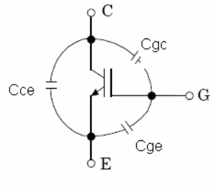
Figure 9: Internal stray capacitances in an IGBT
•
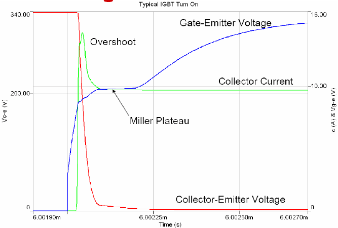
IGBT Turn-On
When a positive voltage is applied on the gate (V
GE
) a current (I
G
) will start to flow into
the gate through the gate resistor R
G
charging the C
ge
capacitor and the voltage rises
exponentially over the capacitor until reaching V
GE(th)
. The Miller effect capacitance
(C
gc
)at this point does not contribute much.
Beyond this point the collector current (I
C
)
starts to increase quickly and linearly to an over-shoot level depending on the
semiconductor structure and the external circuit
.
The gate current decreases to a level
where it stabilizes as the V
GE
reaches the Miller plateau since the C
gc
now gets charged
instead of C
ge
due to the low voltage at the collector. Since the voltage on the collector is
decreasing the voltage on the gate remains rather constant when charging the C
gc
but
increases again after the V
CE
reaches the V
CE(sat).
To finally stop at the maximum V
GE
when both the gate capacitors are fully charged. The speed of the whole Turn-On process
is directly linked to the gate resistor R
g
, a smaller resistor speeds up the process while
causing excessive oscillations or voltage spikes in the circuit. If a snubber circuit is used
it can help to resize the components through filtering out unwanted parts of the signal and
then be able to reducing the gate resistor and make the switching process faster. Although
minimizing stray inductances in wiring and coils is the most effective way of reducing
noise without particular setbacks except practical. On the other hand a larger resistor
slows down the circuit but causes much less noise and voltage transients [9].
11
Figure 10 : Typcial IGBT Turn-on
The dissipated energy during each Turn-On can be calculated from the triangle infolded
by the collector current I
C
and the collector-emitter voltage V
CE
times the time period.
•
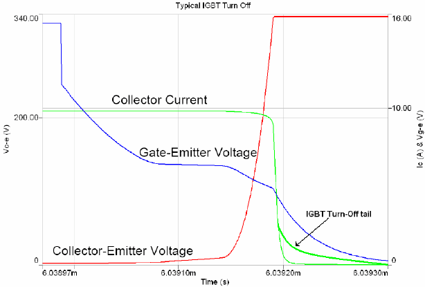
IGBT Turn-Off
During Turn-Off the gate voltage turn to zero and current start to flow from the gate
through the gate resistor, discharging both the gate capacitances, C
ge
and C
ce
until the
Miller plateau is reached. Changing the gate resistor does not change the time of the
process like it did for the Turn-On except in a pure MOSFET where it is possible to
decrease Turn-Off time by reducing this resistor [9]. Then the collector-emitter voltage
(V
CE
) starts to increase until reaching the DC-bus voltage. The gate-emitter voltage (V
GE
)
continues to decrease until passing the threshold voltage (V
GE(th)
) and turning the IGBT
off. Due to the bipolar part of the IGBT a current tail will arise as shown in the figure
below, inflicting additional power loss. The current tail is highly unwanted but is very
hard (impossible today), to eliminate completely.
12
Figure 11 : Typical IGBT Turn-Off
The losses are calculated in the same manner as during Turn-On, the triangular area
infolded by the collector current and the collector-emitter voltage. In addition there is the
current-tail area multiplied by the collector-emitter voltage. In datasheets the dissipated
energy due to the current-tail is often included in the total Turn-Off energy.
2.3.1.2. MOSFET
A power Metal Oxide Semiconductor Field Effect Transistor (MOSFET) is just like a
regular small signal MOSFET but larger in every sense. Larger current and higher
voltages causes the internal capacitances and other critical parameters to suffer increases
both switching and conduction losses. Even though slower than a signal MOSFET it is
definitively faster than any IGBT. The appearance of the Turn-On and Turn-Off graphs
for the MOSFET is very similar to the ones of the IGBT except for a much faster process
and there are no current tails during Turn-Off. In addition, altering the gate resistor can
reduce both Turn-On and Turn-Off time unlike the case with the IGBT where the latter
was somewhat unchangeable. Even if the MOSFET is much faster it suffers large losses
during forward conduction, at least when operating in high voltage applications, this
partly due to the internal resistance growing exponentially with the rated V
DS
as
described by 2.3.1.1.
α
DSonDS
VRR
0)(
=
(2.3.1.1)
Where
6.1≈
α
, V
DS
is the maximum rated voltage and R
0
the initial resistance [9].
This resistance along with the current forms up the voltage drop over the junction as in
2.3.1.2.
α
DSDonDSDsatDS
VRIRIV
0)()(
==
(2.3.1.2)
13
As seen the forward voltage drop increases very quickly with increasing current and
especially the V
DS
voltage. The consequence of this is the inability to reach high
efficiency while operating under high voltages and large currents since the resistance
does not become small enough to compensate for the vast
2
D
I term. This loss is the
dissipated power as shown as in equation 2.3.1.3.
)(
2
onDSDcond
RIP =
(2.3.1.3)
2.3.1.3. BJT
The power Bipolar Junction Transistor (BJT) is one of the components forming the
IGBT. The benefits of using a BJT are its capability of handling high currents and high
forward voltages even if the reverse voltage capabilities are limited. The forward
saturation voltage is almost independent on the current which keeps the conduction loss
at a low level. In opposite to the MOSFET and the IGBT the BJT is a current controlled
device and high power devices usually have a very low HFE
1
, usually a value around 10
for a 10kW application.
This demands very high currents from the driver to saturate the BJT as an unsaturated
device will result in an unwanted high power dissipation most likely to cause failure in
the device. The high base current along with a switching speed near the one of the IGBT
makes the BJT an unsuitable device for this application.
2.3.2. Free-wheeling-diodes
A Free Wheeling Diode is an electronic component used to avoid damage to switching
transistors by reversing load current induction. When switching off an inductive load, the
current cannot go to zero in zero time since there is some energy stored in the magnetic
field. The coil produces a high voltage large enough to let the current continue to flow
over the contact gap, possibly causing permanent damage to the transistor as well as
radiating radio waves. The free wheeling diode is connected anti-parallel with the
transistor and by doing so it doesn't conduct normally as illustrated in figure 12:
Figure 12: IGBT with FWD
If the coil is switched off, the voltage across the coil reverses to maintain the direction of
the current. Now the diode carries the current until the energy is consumed by the inner
resistance of the coil and the forward voltage drop of the diode. This dissipated energy in
the diode is depending on the forward voltage as well as the switching characteristics of
the diode. Because of this, low forward voltage and small stray capacitances are wanted
1
Forward current gain
14
as well as low reverse recovery time which are characteristics that usually contradict each
other. The reverse recovery time is the time taken from forward conduction to blocking in
the reverse direction, this time directly causes loss on the circuit.
2.3.2.1. Silicon Schottky
Usually Schottky diodes are used which have very low reverse recovery time, slightly
lower forward voltage drop and being much faster (much lower stray capacitance)
compared to conventional diodes, although they have low maximum reverse voltage and
a relatively high reverse leakage current that also increases with increasing temperature
which makes them a bad choice in high voltage and high temperature applications.
2.3.2.2. Silicon Carbide Schottky
Since some ten years back other interesting materials are being researched. Diodes made
of Silicon Carbide have proven to have excellent characteristics for high voltage, high
frequency and high temperature. The reverse leaking current is up to 40 times less than
for a regular Shottky, directly reducing losses, reverse voltage up to 1200 V and
extremely low reverse charge as a result of junction capacitance, not stored charge. The
setback is high price and a relatively high saturation voltage, introducing increased loss
when conducting. By having high thermal conductivity and nearly no thermal runaway
also makes the Silicon Carbide the best choice in applications with high temperature.
With special packing junction operating temperatures as high as 500 °K (227 °C) is made
possible which opens up for a wide range of applications. The reverse recovery loss is
usually a significant part of the total switching loss in a hard switched
2
IGBT and by
almost reducing it to zero great reductions in dissipated effect and heat can be made.
2.3.3. Rectifier
The rectifier forms a direct current from an alternating current, in this application from
three phase shifted sources of alternating current. In this case a 6-pulse rectifier model
has been chosen due to its simplicity. However, when handling disturbances on the main
grid a 12-pulse rectifier bridge is to prefer since it heavily reduces harmonics which
otherwise will require large filters. A simulation has been made using Matlab with
Simulink where a 6-pulse rectifier is used and the resulting voltage frequency spectrum
on the grid is measured, see Appendix C1 and C2. Analogous the same measures are
done using a 12-pulse rectifier where it is observed that the noise due to harmonics is
significantly lower, see Appendix C4 and C5. The setback of the 12-pulse bridge is the
needed high power transformer and an additional 6- pulse bridge, together largely
contributing to additional weight. The mean voltage archived on the DC side is calculated
as a combination of all the input voltages as seen in equation 2.3.3.1 [12]:
π
π
40023
23
_
××
=
××
=
−LL
AVEDC
V
V ≈540 V (2.3.3.1)
2
Switching with no snubber circuits or filters and an inductive load

15
This is an average voltage and it will actually oscillate between 490 and 566 volts at the
input frequency multiplied by six demanding a filter to provide a fixed voltage. For a
10kW application the maximum DC-bus current will be as large as 18.5A with
reservation for the result of the DC-bus filter temporarily capable of supplying more than
18.5A The choice of a rectifier bridge is mainly focused on low energy loss and weight
where low energy loss needs less cooling and therefore less weight although in some
applications disturbances and harmonics will cause problems and has to be given higher
priority. However the weight and size of the rectifier itself has in some cases proven to
differ a lot. The ability to withstand heat and to remove this heat should also be taken into
consideration, represented by the thermal resistance of the package. The layout of the
rectifier diodes can be found in figure 13 (encircled):
Figure 13: Overveiw of the rectifier

16
2.4. Filters
2.4.1. Input filters
The non-linear nature of the converter with especially its rectifier and the inductive load
will form a load on the main grid that is far from ideal
3
. Noise generated back on the grid
is a problem for all the other connected equipment but will also emit RMI if not protected
either by shielded wires or an input filter that compensating for this behavior. Usually it
exist a lot of regulations concerning how inductive a load can be and how much noise a
load can inflict, especially in scenarios where the main supply is weak
4
and where it
drives sensitive electronic equipment, such as in an aircraft or other vehicles.
In the scenario covered by this master-thesis a 400 Hz supply is given which implies that
it should not contain high magnitude components at other frequencies. Because of this a
band-pass filter has to be implemented at the input to reduce the magnitude of unwanted
components reflected back to the supply. The components are the fundamental frequency
component and its harmonics of order 6 k±1
5
. This periodic order due to the switched
operation of the line commutated rectifier, in this case a three-phase diode bridge. The
currents harmonics can further be resolved into sequences according to the following
table:
Sequence Harmonics
Positive 1,7,13,19,…
Negative 5,11,17,23,…
Table 1 : Input current harmonics
Usually it is trivial to filter out these harmonics but the high power application along
with the low weight goal makes it difficult to remain within the SOA of all the
components.
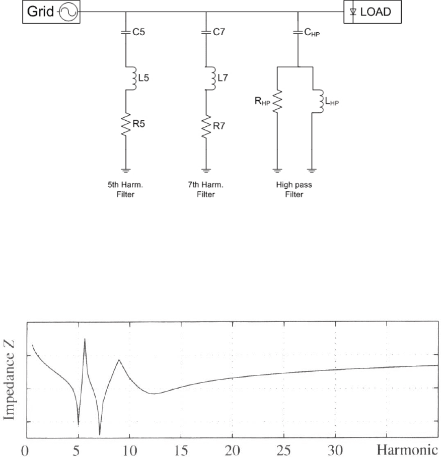
In figure 14 is the schematic of a simple input filter that attenuates the first two harmonic
components of the current as well as a wide range of high frequency noise. More filters
can be added to filter out additional harmonics but will add weight and volume to the
device. How much attenuation of respective harmonics is demanded is usually set by the
environment. In an aircraft there is usually very sensitive equipment on a weak power
source increasing the needs for good filtering. Most of the regulations used and followed
by SAAB AB are found in MIL-STD-704 produced by the US department of defense
[19]. Too some extent high frequency components emitting radio waves can be contained
using shielded cables.
3
Ideal is a purely sinusoidal current
4
The source is considered weak if the voltage is reduced significantly when loaded
5
K is any positive integer, which means the orders can be as in table 1
17
Figure 14 : Input filter
As it is hard to analytically calculate the behavior of currents and voltages in the filter
components an iterative approach using extensive simulations is usually taken. This is
due to the analytical result being valid only during the steady state and not during start up
or shutdown where surge currents will occur. These surge currents can cause failure or
reduce lifetime in the filter components and especially in the electrolyte capacitor if not
dimensioned properly.
Figure 15 : Typical impedance for input filter vs. harmonics of grid frequency
The amounts of harmonics reflected back from the inverter to the grid is also dependant
on the LC-filter between the rectifier and the switching bridge. This because currents
through the diodes is dependant on the charging currents of the capacitor which itself is
dependant on the choke inductor and the surge limiter. These harmonics are also hard to
analytically estimate and a system level simulation is favored. To estimate the harmonics
in this converter Matlab with Simulink will be used where the entire converter is modeled
and the frequency spectrum on the input is measured. When having the high amplitude
harmonics determined a band-stop filter for each undesired harmonic has to be
implemented with appropriate attenuations. This frequency spectrum measurement can be
seen in Appendix C1 where the harmonics can easily be identified. The maximum
allowed disturbance can be found in the MIL-STD-704D military standard document
18
[19]. In table 2 the larger harmonics in comparison with the maximum allowed levels and
the required attenuation can be viewed:
Harmonic # Frequency(hz) Amplitude peak/RMS V Allowed level RMS Attenuation dB
fundamental 400 550/388 -
5 2000 48/34 20 2.3
7 2800 16/11.3 20 -
11 4400 20/14 20 -
13 5200 14/10 16 -
17 7800 8/5.7 12 -
Table 2 : Voltage harmonics on grid
As in table 2 the given voltages arise due to harmonic currents through the source usually
represented by a generator the respective current components can be filtered instead. This
is carried out as explained in figure 14 with serial RLC circuit connected to next phase or
virtual ground. The impedance of the RLC circuit is usually calculated as in 2.4.1.1:
()
2
2
1
⎟
⎠
⎞
⎜
⎝
⎛
−+=
C
LRRLC
Z
ω
ωω
(2.4.1.1)
The RLC impedance is at minimum at the resonance frequency
LC1=
ω
where it
assumes the value R. This value R limits the current at the filtered frequency preventing it
to become unnecessary large. The L and C values can be chosen somewhat arbitrary as
long as the resonance frequency is the correct one. The current harmonics can be found in
appendix C along with the voltage harmonics.
As seen in table 2 the voltage at the 5
th
harmonic caused by its respective harmonic
current has to be reduced to 59% relying on the filter to consume this excessive current.
It is also the only component needed to be individually reduced, the higher frequency
components are attenuated with a high-pass filter as illustrated in figure 14. Given the
RMS voltage 34 V and the RMS current 2.52 A at the frequency 2000 Hz of which the
filter will consume 41 % gives the value of R according to 2.4.1.2:
Ω=
×
=
×
= 9.32
41.052.2
34
41.0
_
_
rmsharmonic
rmsharmonics
I
V
R
(2.4.1.2)
Assuming the value 100µH for the inductor L gives along the resonance frequency 2000
Hz the capacitor C a value of 63 µF. The estimated voltage and current give a power loss
of 34W. Although this is per phase and should be multiplied by three when added to the
complete system. This has to be done with the components as well, adding weight and
space. The combined weight of the 5
th
harmonic filter per phase is estimated to 120g
which gives a total of 360g. The dimension can be seen in the layout sketch, in Appendix
F

19
The high-pass filters are calculated in the same manner but when calculating loss a few
more harmonic components are added, although smaller in magnitude. A 10Ω with a
100nF capacitor in series nearly does not interfere with the 5
th
harmonic filter but filter
higher order harmonics rather effectively. The accumulated power loss is estimated to be
about 3 watts per phase which will all be dissipated in the resistor. The estimated weight
per phase is 11 g, giving a total of 33g.
Component Filter Ratings Manufacturer
and Model
Mass
(g)
Volume
(mm
3
)
Power
loss (W)
R 5
th
harmonic
33Ω ARCOL HS 3*31 3*(29x70x15)
L 5
th
harmonic
100μH Pulse
L100
3*19 3*(15x25x24)
C 5
th
harmonic
70μF EVOX RIFA
PEH200
3*70 3*(35x51)
3*34
R High-pass 10Ω VITROHM
KH
3*5 3*(8x8x22)
C High-pass 100nF EVOX RIFA
PHE845
3*7 3*(11x22x26)
3*3
Table 3 : Input filter components
2.4.2. DC-bus filter
2.4.2.1. Capacitor bank
Because of the nature of the rectifier the voltage on the DC-bus will vary with time, but
not only because of this but from the pulse shape of the output current as well. Due to this
a LC-filter is needed to stabilize the voltage as well as providing a current buffer. The
performance of the filter is limited by the weight and cost always wanted to be kept low.
As electrolyte capacitors are used the lifetime is limited and estimated using a simple
model to assure lifetime long enough according to regulations.
The dimensioning of the components requires some extensive calculations which in detail
will be explained in this chapter starting with reviewing the provided parameters.
•
Main power grid: 400VAC, 400Hz three-phase, 560VDC maximum
•
Capacity: 10kW with 10kHz switching frequency
•
Full wave bridge rectifier: 400*6 Hz ripple frequency
•
Maximum allowed ripple voltage: 3% of average DC-bus voltage i.e. 16 V.
•
Common MTBF: 5000 hours of flight/operation
Assuming all the energy is stored in the capacitor bank a calculation gives according to
the well known formula of the potential energy in a capacitor
2
2
1
VCE
totcap
×= (2.4.2.1.1)