Buschow K.H.J. (Ed.) Concise Encyclopedia of Magnetic and Superconducting Materials
Подождите немного. Документ загружается.


13. Three-terminal Spin Electronic
Device Variants
Ounadjela and Tiusan (1999) have proposed a neat
and versatile metallic spin-tunnel transistor with
particular relevance to three-terminal spin-tunnel
MRAM application. The device has two tunnel bar-
riers between emitter/base and base/collector respec-
tively. It operates on the SPICE principle and has
numerous variants which differ in respect of the pre-
cise location of the encoder and decoder electrodes
relative to the collector structure.
Mizushima et al. (1998, 1999) have also produced a
variety of interesting tunnel transistor designs, again
operating on the SPICE principle but, unlike the
Ounadjela/Tiusan device they comprise semiconduc-
tor collector elements.
14. Spin Electronics in Carbon Nanotubes
An unusual but prophetic venture in spin electronics
is the use of single-wall carbon nanotubes as spin
conductors (Alphenaar et al. 2000). Surprisingly it is
discovered that the spin diffusion lengths in such
tubes are many tens of nanometers and their future
application looks promising.
15. Voltage-induced Switching
Interesting predictions have been made with respect to
the simple RKKY-coupled GMR trilayer structure to
the effect that the interlayer magnetic coupling could
be changed in sign by application of sufficient voltage
across the structure (You and Bader 1999). The object
of such endeavor is to produce a magnetic memory
element or switch whose transport in one dimension
may be altered by magnetic switching which is induced
not by external magnetic fields but rather by an electric
potential in n orthogonal direction. This remains to be
demonstrated experimentally.
16. Current-induced Switching
Current-induced switching of a spin electronic struc-
ture has also been predicted and experimental results
are available which appear to confirm it. The prin-
ciple harks back to an idea of Luc Berger (Myers
et al. 1999) in which he examines the relationship
between current density and the torque/force on a
ferromagnetic domain wall. If a sufficiently large
spin-polarized current is incident normally on a
domain wall, the spin angular momentum exerts a
torque which twists the spins and hence effectively
causes the wall to move. When implemented in ferro-
magnetic nanocontacts, the effect is attractive as an
operating principle for simple MRAM memory ele-
ments (Coey 2001).
17. Quantized Conductance
When a point contact with dimensions of atomic size
is made between two metallic nanowires, the lateral
confinement causes mutual distancing of the k-states
in a plane perpendicular to the direction of current
flow (Ott et al. 1998). This means that only a small
number of conductance channels are below the metal
Fermi surface. By varying the contact width, the
individual conductance quanta may be observed.
Simple theory suggests that in the case of spin asym-
metric contacts, the quanta should be halved, but so
far this effect has eluded observation.
18. Measuring Spin Asymmetry
Various techniques are used for estimating the spin
asymmetry of spin electronic materials. They include
spin-resolved photoemission (Park et al. 1998), And-
reev reflection (Soulen et al. 1998), measurement of
the Zeeman effect of chemical potential (Sirisathitkul
et al. 2001b), and by spin tunneling to a material with
100% polarization (de Teresa et al. 1999). The last
tunneling technique relies on the control electrode
genuinely behaving as if it is 100% polarized. Merely
because its bulk bandstructure is fully polarized is no
guarantee of this. As discussed above, the polariza-
tion which magnetic electrodes manifest for tunneling
purposes is found to be a function of the magnetic
metal/insulator combination, not just of the magnetic
metal itself. Thus, it is important that the control
electrode is always accompanied by the same insula-
tor. This casts a new light also on the other meas-
urement techniques for measuring spin polarization
and shows not only the importance of establishing
exactly what they are measuring, but it also begs the
question as to what we really should be trying to
measure for practical purposes.
19. Competing Magnetotransport Phe nomena
There exists a large number of magnetotransport ef-
fects which are not strictly spin electronic in origin
but which nonetheless can display similar character-
istics. They include anisotropic magnetoresistance,
Hall effect and anomalous Hall effect.
In this category, an interesting and potentially use-
ful giant magnetotransport effect has been observed
in a ferromagnet/semiconductor structure in which
arrays of submicron ferromagnets are fabricated on a
heterostructure containing a near surface two-dimen-
sional electron gas. The magnetoresistance arises
from electrons propagating in open orbits along lines
of zero magnetic field (Nogaret et al. 1997).
20. Measurement Artefacts
In spin electronics the currents and voltages meas-
ured are frequently small and this heightens the need
620
Magnetic Reco rding Systems: Spin Electronics

for vigilance against interference from rival transport
effect and spurious artefacts. The most obvious
sources of such trouble are radiated electrical noise
and earth loops. However there is also a more subtle
artefact which may occur in a.c. transport measure-
ments in applied magnetic field if the flying leads to
the sample are free to move. The current carrying
wires are subject to a harmonic torque in a magnetic
field and if they are capable of mechanical displace-
ment this leads to a harmonic flux variation. The
result is a parasitic voltage and hence an apparent
resistance which is proportional to the square of the
magnetic field.
21. Applications of Spin Electronics
Applications to date of spin electronics include hard
disk read heads, advanced high density tape heads,
and various position and motion sensors based on
GMR and high frequency properties of spin elec-
tronic materials. Although not yet commercialized,
spin tunnel MRAM is at an advanced stage of de-
velopment also. More speculative uses with future
potential include applications of spin FETS to quan-
tum information processing and the radiofrequency
ferromagnetic single electron transistor.
Bibliography
Alphenaar B W, Tsukagoshi K, Ago H 2000 Spin electronics
using carbon nanotubes. Physica E 6, 848–51
Baibich M N, Broto J M, Fert A, Nguyen Van Dau F, Petroff
F, Etienne P, Creuzet G, Friederich A, Chazelas J 1988 Giant
magnetoresistance of (001)Fe/(001)Cr magnetic superlattices.
Phys. Rev. Lett. 61, 2472–5
Barnard J A, Waknis A, Tan M, Haftek E, Parker M R,
Watson M L 1992 Giant magnetoresistance observed in
single layer Co–Ag alloy films. J. Magn. Magn. Mater. 114,
L230–4
Barnas J, Fert A 1998 Effects of spin accumulation on single-
electron tunneling in a double ferromagnetic microjunction.
Europhys. Lett. 44, 85–90
Barthelemy A, Fert A 1991 Theory of the magnetoresistance in
magnetic multilayers analytical expressions from a semiclas-
sical approach. Phys. Rev. B 43, 3124–9
Bean C P, Livingstone J D 1959 J. Appl. Phys. 30, 120
Berger L 1991 Galvanomagnetic voltages in the vicinity of a
domain wall in ferromagnetic thin films. J. Appl. Phys. 69
(3), 1550–5
Berkowitz A E, Mitchell J R, Carey M J, Young A P, Zhang S,
Spada F E, Parker F T, Hutten A, Thomas G 1992 Giant
magnetoresistance in heterogeneous Cu–Co alloys. Phys.
Rev. Lett. 68, 3745–8
Cabrera G G, Falicov L M 1974 Phys. Stat. Sol. (b) 61, 539
Chui S T 1997 Bias dependence in spin-polarised tunneling.
Phys. Rev. B 55 (9), 5600–3
Coey J M D 2001 Magnetic peanut memory device. Irish Patent
filing
Daniel D, Gregg J F, Thompson S M, Coey J M D, Fagan A,
Ounadjela K, Fermon C, Saux G 1995 Giant magnetother-
mal resistance. J. Magn. Magn. Mater. 1404, 493–4
Datta S, Das B 1990 Electronic analog of the electrooptic
modulator. Appl. Phys. Lett. 56, 665–7
de Groot R A, Mueller F M, van Engen P G, Buschow K H J
1984 Half-metallic ferromagnets and their magneto-optical
properties. J. Appl. Phys. 55 (6), 2151–4
De Teresa J M, Barthelemy A, Fert A, Contour J P, Montaigne
F, Seneor P 1999 Role of metal-oxide interface in deter-
mining the spin polarisation of magnetic tunnel junctions.
Science 286, 507–9
Devoret M H, Grabert H 1992 Single Charge Tunneling. Ple-
num, New York
Dieny B, Speriosu V S, Parkin S S P, Gurney B A, Wilhoit D R,
Mauri D 1991 Giant magnetoresistance in soft ferromagnetic
multilayers. Phys. Rev. B 43, 1297–300
Dubois S, Piraux L, George J M, Ounadjela K, Duvail J L, Fert
A 1999 Evidence for a short spin diffusion length in perm-
alloy from the giant magnetoresistance of multilayered nano-
wires. Phys. Rev. B 60 (1), 477–83
Fert A, Duvail J-L, Valet T 1995 Spin relaxation effects in the
perpendicular magnetoresistance of magnetic multilayers.
Phys. Rev. B 52, 6513–21
Fiederling R, Keim M, Reuscher G, Ossau W, Schmidt G,
Waag A, Molenkamp L W 1999 Injection and detection of a
spin polarised current in a light emitting diode. Nature 402,
787–90
Flatte M E, Byers J M 2000 Spin diffusion in semiconductors.
Phys. Rev. Lett. 84 (18), 4220–3
Gehring G A, Gregg J F, Thompson S M, Watson M L 1995
Electron spin depolarisation in granular magnetic systems.
J. Magn. Magn. Mater. 1404, 501–2
Gerritsen A N 1959 Physica 25, 489–502
Giaever I, Megerle K 1961 Phys. Rev. 122 (4), 1101
Gregg J F, Allen W, Ounadjela K, Viret M, Hehn M, Thomp-
son S M, Coey J M D 1996 Giant magnetoresistive effects in
a single element magnetic thin film. Phys. Rev. Lett. 77 (8),
1580–3
Gregg J F, Allen W D, Viart N, Kirschmann R, Sirisathitkul C,
Schille J-P, Gester M, Thompson S M, Sparks P, da Costa V,
Ounadjela K, Skvarla M 1997 J. Magn. Mater. 175, 1–9
Hagele D, Oestreich M, Ruhle W W, Nestle N, Ebert K 1998
Spin transport in GaAs. Appl. Phys. Lett. 73 (11), 1580–2
Hammar P R, Bennett B R, Yang M J, Johnson M 1999 Ob-
servation of spin injection at a ferromagnet–semiconductor
interface. Phys. Rev. Lett. 83 (1), 203–6
Jia Y Q, Shi R C, Chou S Y 1996 Spin-valve effects in nickel/
silicon/nickel junctions. IEEE Trans. Magn. 32 (5),
Johnson M 1993 Bipolar spin switch. Science 260 (5106), 320–3
Johnson M, Silsbee R H 1985 Interfacial charge-spin coupling:
injection and detection of spin magnetisation in metals. Phys.
Rev. Lett. 55 (17), 1790–3
Julliere M 1975 Phys. Lett. A 54, 225
Kikkawa J M, Awschalom D D 1999 Lateral drag of spin
coherence in gallium arsenide. Nature 397, 139–41
Lee S F, Pratt W P, Yang Q, Holody P, Lololee R, Schroeder
P A, Bass J 1993 2-Channel analysis of CPP-MR data for
Ag/Co and AgSn/Co multilayers. J. Magn. Magn. Mater.
118, L1–5
Loraine D R, Pugh D I, Jenniches H, Kirschman R, Thompson
S M, Allen W, Sirisathitkul C, Gregg J F 2000 Effect of
silicon crystal structure on spin transmission through spin
electronic devices. J. Appl. Phys. 87 (9), 5161–3
Mizushima K et al. 1998 US Patent 5747859
Mizushima K et al. 1999 US Patent 5973334
Monsma D J, Lodder J C, Popma J A, Dieny B 1995 Perpen-
dicular hot-electron spin-valve effect in a new magnetic field
621
Magnetic Reco rding Systems: Spin Electronics

sensor the spin-valve transistor. Phys. Rev. Lett. 74 (26),
5260–3
Mott N F 1936 Proc. R. Soc. 153,69
Myers E B, Ralph D C, Katine J A, Louie R N, Buhrman R A
Current-induced switching of domains in magnetic multi-
layer devices. Science 285 (5429), 86770
Nogaret A, Carlton S, Gallagher B L, Main P C, Henini M,
Wirtz R, Newbury R, Howson M A, Beaumont S P 1997
Observation of giant magnetoresistance due to open orbits in
hybrid semiconductor/ferromagnet devices. Phys. Rev. B 55
(24), R16037–40
Ohno Y, Young D K, Beschoten B, Matsukura F, Ohno H,
Awschalom D D 1999 Electrical spin injection in a ferro-
magnetic semiconductor heterostructure. Nature 402, 790–2
Ott F, Barberan S, Lunney J G, Coey J M D, Berthet P, de
Leon-Guevara A M, Revcolevschi A 1998 Quantised con-
ductance in a contact between metallic oxide crystals. Phys.
Rev. B 58 (8), 4656–9
Ounadjela K, Tiusan C 1999 Dispositif microelectronique a
jonctions tunnel et reseau de memoires et capteur compren-
ant de tels dispositifs. Demande de brevet Francais 9904227
Park J-H, Vescovo E, Kim H -J, Kwon C, Ramesh R, Venk-
atesan T 1998 Direct evidence for a half-metallic ferromag-
net. Nature 392, 7946
Parkin S S P, More N, Roche K P 1990 Oscillations in exchange
coupling and magnetoresistance in metallic superlattice
structures: Co/Ru, Co/Cr and Fe/Cr. Phys. Rev. Lett. 64,
23047
Piraux L, George J M, Despres J F, Leroy C, Ferain E, Legras
R, Ounadjela K, Fert A 1994 Giant magnetoresistance in
magnetic multilayered nanowires. Appl. Phys. Lett. 65 (19),
1–3
Prins M W J, Jansen R, van Kempen H 1996 Spin-polarised
tunneling with GaAs tips in scanning tunneling microscopy.
Phys. Rev. B 53 (12), 8105–13
Renard J P, Bruno P, Megy R, Bartenlian B, Beauvillain P,
Chappert C, Dupas C, Kolb E, Mulloy M, Prieur J, Veillet P,
Velu E 1996 J. Appl. Phys. 79 (8), 5270–5
Sirisathitkul C, Allen W D, Gregg J F, Sparks P D, Coey J M
D, Kirschman R, Thompson S M 2001a Spin blockaded
silicon Schottky barrier. (In preparation)
Sirisathitkul C, Allen W D, Gregg J F, Sparks P D, Coey J M
D, Kirschman R, Thompson S M 2001b Measuring spin
asymmetry via the chemical potential Zeeman shift. (In prep-
aration)
Soulen R J, Byers J M, Osofsky M S, Nadgorny B, Ambrose T,
Cheng S F, Broussard P R, Tanaka C T, Nowak J, Moodera
J S, Barry A, Coey J M D 1998 Measuring the spin polar-
isation of a metal with a superconducting point contact.
Science 282, 85–8
Tang H X, Monzon F G, Lifshitz R, Cross M C, Roukes M L
2000 Ballistic spin transport in a two dimensional electron
gas. Phys. Rev. B 61 (7), 4437–40
Tedrov P M, Merservey R 1971 Phys. Rev. Lett. 26, 192
Tiusan C, Hehn M, Ounadjela K, Henry Y, Hommet J, Meny
C, van den Berg H, Baer L, Kinder R 1999 Artificial antif-
erromagnetic tunnel junction sensors based on Co/Ru/Co
sandwiches. J. Appl. Phys. 85,
Valet T, Fert A 1993 Theory of the perpendicular magnetore-
sistance in magnetic multilayers. Phys. Rev. B 48, 7099–113
van Wees B J, et al. 2000 Comment on observation of spin
injection at a ferromagnet–semiconductor interface. Phys.
Rev. Lett. 84 (21), 5022
Versluijs J J, Bari M A, Coey J M D 2001 Magnetoresistance of
half-metallic oxide nanocontacts. in press
Yang Q, Lee S F, Henry L L, Lololee R, Schroeder P A, Pratt
W P, Bass J 1994 Diffusion length and giant magnetoresist-
ance at low temperatures. Phys. Rev. Lett. 72, 3274–7
You C-Y, Bader S D 1999 Prediction of switching/rotation of
the magnetisation direction with applied voltage in a con-
trollable interlayer exchange coupled system. J. Magn. Magn.
Mater. 195, 488–500
J. Gregg
University of Oxford, Oxford, UK
Magnetic Recording Systems: Spin Valves
The rapid increase in information storage density in
magnetic recording systems over recent years has
been made possible in part by the development of
spin-valve (SV) read heads. These rely on the phe-
nomenon of giant magnetoresistance (GMR), in
which a change in resistance is observed on applica-
tion of a magnetic field (see Giant Magnetoresist-
ance). This article discusses the GMR effect on which
the devices are based, and also the parameters that
are important in consideration of the design of spin-
valve structures, such as the choice of materials for
the various layers in the device, and thermal stability.
The effect of microstructure and of magnetization
reversal on device operation are also discussed.
1. Introduction
A change in resistance on application of a magnetic
field in magnetic materials gives rise to a tremendous
number of applications in the electronics industry.
One of the most spectacular examples is the applica-
tion of giant magnetoresistance in ultrahigh-density
magnetic recording technology, and one of the de-
vices based on this phenomenon is the SV structure
that has applications as read heads (Brug et al. 1996)
in hard disk storage systems or as magnetoresistive
random access memory (MRAM) elements (Daugh-
ton 1997). The rapid increase in interest in these de-
vices has been motivated by the high demand for
improvement in information storage density and per-
formance, mainly for graphics-intensive applications.
Improvements in signal processing and disk media,
plus the development of SV read heads, have allowed
the density to be increased to 50 Gb/in
2
with a pro-
jected obtainable density of 80–100 Gbits/in
2
. The
limits on memory density that can be achieved using
solid-state memory (for example DRAM) means that
there has been renewed interest in the development of
magnetic memory based on the GMR effect, namely
MRAM. In addition, MRAM would be nonvolatile.
2. The GMR Effect
GMR is observed in films consisting of alternate
ferromagnetic (FM) and nonmagnetic layers, as a
622
Magnetic Reco rding Systems: Spin Valves
large change in resistance with applied magnetic field.
The resistance is a function of the relative alignment
of the magnetization in the magnetic layers, and thus
of spin-dependent scattering of the conduction elec-
trons. It was first observed for Fe/Cr multilayers with
thicknesses of a few nanometers.
(For a general description of GMR the reader is
referred to a number of review papers, for example
Dieny (1994).) The GMR ratio is defined as:
DR=R ¼ðR R
P
Þ=R
P
ð1Þ
where R
P
is the resistance for parallel alignment of
the FM layer magnetization directions. The maxi-
mum GMR ratio is observed when
R ¼ R
AP
ð2Þ
where R
AP
is the resistance of the antiparallel mag-
netization configuration.
3. The Spin Valve Structure
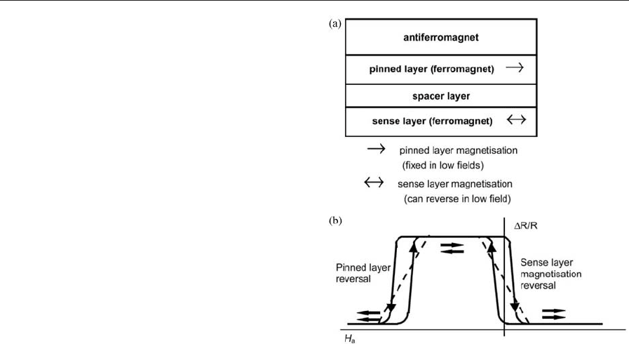
SV structures (see, for example, review of SV struc-
tures in Portier and Petford-Long (1999), however,
offer greater possibilities for development for real
applications than multilayer structures. In their sim-
plest form, a SV consists of two ferromagnetic layers
separated by a nonmagnetic spacer layer. The mag-
netization direction (easy axis) of one FM layer is
fixed by an adjacent antiferromagnetic (AF) layer
(pinning layer) through exchange coupling (see Mul-
tilayers: Interlayer Coupling). The magnetization di-
rection of the other FM layer (sense layer) can be
rotated by applying a small external magnetic field
(of the order of a few oersteds) in the plane of the
layers. A schematic illustrating the structure of a
simple SV is shown in Fig. 1(a).
In a spin valve, unlike in a GMR exchange cou-
pling of the two FM layers across it is small. For a
spin valve, the GMR is linearly dependent on (cos y)
where y is the angle between the sense and pinned
layer magnetizations:
RðyÞ¼R
P
þðR
AP
R
P
Þð1 cosyÞ=2 ð3Þ
When applying the external field perpendicular
to the easy axis, the change in resistance is linear
with low coercivity and a sense layer magnetiza-
tion reversal characterized by coherent rotation (see
Fig. 1(b)). This configuration is used for sensors. The
second commonly used configuration is to apply the
external field along the easy axis direction. In this
case, two remanent states can be stabilized with either
parallel (P) or antiparallel (AP) alignment of the
magnetization of the pinned and sense layers. The
magnetization reversal is then a hysteretic reversal
process, with the P and AP states corresponding
to the minimum and maximum resistance values,
respectively. This is suitable for MRAM devices (high
and low resistance could correspond to ‘‘1’’ and ‘‘0’’
bit states). A GMR ratio of up to 23.4% has been
obtained for a SV structure at room temperature.
Despite the fact that SV materials have been in-
troduced commercially as read heads in the latest
generations of hard disk drives, a number of pro-
blems remain to be solved. These include magneto-
static coupling of the pinned and sense layers, which
leads to an offset of the GMR curve with respect to
remanence, and thus to a need for a higher operating
magnetic field, low exchange coupling between the
pinned and pinning layer for some configurations,
and a reduction in GMR after lithographic process-
ing. Solving these problems requires understanding
the microstructure and local magnetic structure of the
SV films.
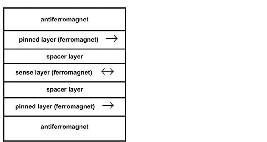
3.1 Microstructure
To enhance the GMR ratio, several different SV
structures have been proposed, for example the ‘‘top’’
SV (see Fig. 1(a)) and the ‘‘bottom’’ SV in which the
layer order is reversed. Changing the deposition order
changes both the crystallographic texture of the film
Figure 1
(a) schematic cross-section through a simple SV
structure, (b) schematic GMR curve for a SV with the
external field applied perpendicular to the easy axis of
magnetization in the pinned layer (- ----) and with the
external field applied parallel to the easy axis of
magnetization in the pinned layer (––––).
623
Magnetic Reco rding Systems: Spin Valves
and the interfacial roughness, which are of crucial
importance in controlling the GMR. Figure 2 shows
a schematic of the dual, or symmetric, SV, which
contains one central FM sense layer and two biased
FM layers. This structure has been found to increase
the GMR ratio up to 23.4% compared with a top SV
made with the same materials which gives only a 10%
GMR ratio. In all cases, the FM material used for the
pinned and sense layers can be either the same or
different, depending on the properties required. The
structures are usually protected from oxidation by a
cap layer.
One of the important requirements in operating SV
structures is to be able to reverse the magnetization of
the sense layer in a low external magnetic field, hence
the use of soft magnetic materials such as Permalloy
(Ni
80
Fe
20
). Cobalt is also widely used and has a
higher saturation magnetization, coercivity, and mag-
netocrystalline anisotropy, particularly for the h.c.p.
structure, which tends to form for layer thicknesses
greater than 4 nm. Sense layer thickness is also im-
portant, with an increase in thickness leading to a
larger grain size and decrease in coercivity. A typical
grain size is about 20 nm for an 8 nm-thick NiFe
sense layer, which gives an optimal GMR ratio.
Another alternative for the pinned layer is to use
an artificial antiferromagnet (AAF) such as Co/Ru/
Co, in which the cobalt layers are antiferromagnet-
ically exchange-coupled across the ruthenium, and
one of the cobalt layers is pinned by an adjacent
AFM material. The net magnetization of the pinned
layer is then close to zero. SVs containing an AAF
show good sensitivity to an external magnetic field
because stray-field coupling between the pinned and
sense layers in lithographically defined elements is
very much reduced.
The spacer layer needs to be very conductive to
reduce spin-independent scattering of the conduc-
tion electrons and is commonly copper, silver, or
gold. Copper is most widely used as its structure
matches well (1.85% mismatch) with those of cobalt
or Ni
80
Fe
20
. Intermixing between NiFe and copper
can lead to the formation of a paramagnetic interfa-
cial alloy layer, resulting in spin-flip scattering and
loss of GMR, but this can largely be avoided by in-
serting a thin cobalt layer at the NiFe/Cu interface.
The GMR properties of SVs are very dependent on
the nature of the interfaces between the layers, and
three different types of interlayer coupling can arise
across the FM/NM/FM interfaces:
*
FM exchange coupling between the FM layers
through pinholes in the spacer, although this is
largely avoidable for spacer layers thicker than about
1.5 nm.
*
Magnetostatic ‘‘orange-peel’’ coupling which
arises because of the waviness of the FM layer/spac-
er layer interface leading to free magnetic poles of
opposite sign across the spacer layer, for which Ne
´
el
proposed a model relating the period and the ampli-
tude of the waviness to the coupling strength.
*
An oscillatory Ruderman-Kittel-Kasuya-
Yosida (RKKY-like) coupling which is dependent
on the spacer layer thickness and decays with in-
creasing thickness in an oscillatory manner between
FM and AFM coupling. The spacer layer thickness is
usually chosen to be high enough that the RKKY
coupling is negligible, but if it is too high, increased
spin-independent scattering of the conduction elec-
trons and increasing shunting of the current through
the spacer layer lead to a decrease in GMR. The op-
timum thickness has been found to be B2.5–3 nm.
One of the key parameters for a SV device is the
strength of the exchange coupling (H
ex
) between the
antiferromagnetic (pinning) and pinned layers (see
Nogue
´
s and Schuller 1999) for a review of exchange-
biasing effects). The exchange field is set by applying
a magnetic field during deposition or postdeposition
anealing in order to align the magnetization of the
first monolayer of the AFM material with that of the
adjacent FM layer. The coupling strength depends on
the AFM material used and on its microstructure,
with the most commonly used materials being FeMn,
NiMn, and IrMn, although other materials such as
CoO, NiO, TbCo, a-Fe
2
O
3
, and other manganese al-
loys are being considered. An increase in H
ex
and in
the pinned-layer coercivity are observed when reduc-
ing the thickness of the FM material, and an increase
of H
ex
and of the blocking temperature (the temper-
ature above which no exchange field is observed)
have been linked to an increase in grain size.
Figure 2
Schematic of dual SV structure.
624
Magnetic Reco rding Systems: Spin Valves

The surface topology is also important since a
smoother interface between the pinning and pinned
layers tends to improve H
ex
.
The first systems to be studied used FeMn because
it is structurally very similar to the FM and spacer
layers. However, H
ex
(B150 Oe) and the blocking
temperature (B 150 1C) are relatively low and its cor-
rosion resistance is not very high (this can be im-
proved by adding chromium, iridium, platinum,
rhodium, or ruthenium during deposition). The most
promising AFM material to date is MnNi with H
ex
up to 500 Oe after annealing, a blocking temperature
of B380 1C, a reasonable corrosion resistance, and
very good thermal stability. The as-grown MnNi is
cubic and nonmagnetic, but an anneal at about
220 1C for 1 hour leads to a phase transformation to
the antiferromagnetic face-centred-tetragonal (f.c.t.)
phase. A difficult task is to determine the real pro-
portion of MnNi grains with the f.c.t. structure com-
pared to those still with the f.c.c. structure.
The most common deposition techniques used for
fabricating SVs are ion-beam deposition (IBD), DC
magnetron sputtering, and MBE. MBE-grown films
tend to be epitaxial and single crystal, whereas the
sputtered films are polycrystalline. Films grown by
IBD usually have higher resistivities and lower GMR
than DC magnetron-sputtered films because of
greater intermixing between the layers. Polycrystal-
line films tend to show better GMR properties than
MBE-grown films, but a good /111S texture be-
tween the pinning and the pinned layers is preferable
for a strong pinning effect. In addition, the coercivity
of the sense layer is lower for a well-textured film,
which enables a rapid transition between the P and
AP states for MRAM applications.
To increase the grain size and degree of texture
in the film, a seed layer such as niobium, tantalum,
titanium, or zirconium is commonly used. Tantalum
is the most widely used, as it induces the /111S tex-
ture for most of the various FM materials used as
the sense layer resulting in a columnar growth from
bottom to top in the SV structure. In addition, the
tantalum/FM layer interface usually has a good ther-
mal stability. However, an intermixed, magnetically
‘‘dead’’ layer of a few monolayers is often observed
between the seed and the FM layer. Note that for
bottom SV structures it is sometimes necessary to
deposit a thin FM layer below the AFM material to
obtain a good crystallographic texture.
4. Thermal Stability
The GMR amplitude decreases linearly with temper-
ature by a factor of about three from 4 K to room
temperature. The main effect is magnon scattering of
the conduction electrons in the bulk of the FM layers
which has been correlated to the Curie temperature of
the FM material, but another contribution will be
phonon scattering in the NM layer preventing the
exchange of conduction electrons between the sense
and pinned layers. Operating a SV structure at ele-
vated temperatures thus leads to a decrease of the
GMR effect, but the critical temperature above which
the linear dependence is lost depends strongly on the
structure used.
The critical temperatures are much lower than in
bulk materials because of the numerous grain bound-
aries whose diffusion coefficients are much higher than
the bulk values, favoring layer interdiffusion at lower
temperatures. In addition, changes to the interface
between the seed layer and the sense layer can degrade
the GMR effect following annealing, because of the
formation of a high-resistivity alloy at the seed layer/
FM interface. The cobalt/copper system is more
thermally stable than other systems such as NiFe/
copper, for example, because cobalt/copper is a phase-
separating system and, because the Curie temperature
of cobalt is high in comparison with NiFe, although
the GMR properties are not as good.
5. Micromagnetic Considerations
5.1 Sense-layer Reversal
One of the important parameters for the operation of
a SV is the magnetization-reversal mechanism of the
sense layer, because of its influence on the GMR re-
sponse of the SV. If the applied field is along the easy
axis direction, the reversal of the sense layer magnet-
ization occurs via domain wall motion for NiFe, and
by magnetization rotation mechanisms for cobalt,
with a higher reversal field for the cobalt-based SVs.
This is expected because of the higher saturation
magnetization and magnetocrystalline anisotropy of
cobalt. However, some other features can be seen,
which are directly attributable to the FM interlayer
coupling. First, the domain structure for a NiFe-
based SV is more complex than for a single NiFe film.
In addition, domain walls are observed to lie at an
angle with respect to the easy axis direction because
of the residual torque associated with coupling to the
pinned layer.
Third, the P–AP and AP–P reversal are not sym-
metric, with more magnetization rotation observed
for the AP–P reversal. This is a result of the combi-
nation of the unidirectional anisotropy imposed by
the exchange field of the AFM layer on the pinned
FM layer and the FM ‘‘orange-peel’’ magnetostatic
coupling between the pinned and sense layers.
A further important feature is that the hysteresis
loop is shifted with respect to zero field, and there are
a number of terms that contribute to this effect. The
first of these is the orange-peel coupling (H
FM
), which
is FM in nature. Second, there is a magnetic field
induced by the current passing through the device
(H
I
), whose effect depends on the direction of current
flow and its magnitude.
625
Magnetic Reco rding Systems: Spin Valves

A simple model based on Ampere’s law:
H
I
¼ 0:75Ið4p 10
3
Þ=2h ð4Þ
where I is the current and h is the height (width) of
the element, provides good agreement with experi-
mental observations. Third, magnetostatic stray-field
coupling occurs at the edges of a lithographically
defined SV element because of the demagnetizing
field (H
d
) between the pinned and sense layers. This
phenomenon becomes of primary importance as the
element size is reduced and is strongly dependent
on element size and shape. The stray-field coupling
is AFM in nature, and H
d
can be simply estimated
using:
H
d
¼ð4pMt=hÞu
y
ð5Þ
where M and t are the saturation magnetization and
thickness of the sense layer, respectively, h is the
width of the element, and u
y
is a unit vector in the
easy axis direction. A possible expression for the off-
set field (H
off
), by which the GMR curve is displaced
from zero, can then be given as:
H
off
¼ H
FM
þ H
I
þ H
d
ð6Þ
As mentioned previously, a decrease in sense-layer
thickness and/or the use of an AAF as the pinned
layer lead to a substantial reduction of the stray field
coupling. Flattening the FM/NM/FM layer inter-
faces, for example by the use of a surfactant such as
indium, can reduce the orange peel coupling. H
off
should be kept as low as possible to reduce the ex-
ternal field that must be applied to reverse the sense
layer magnetization.
Finally, 3601 domain walls are often observed,
mainly at the end of the P–AP transition, which
consist of a pair of very close domain walls separated
by a very narrow region of film in which the mag-
netization in the two FM layers is still in the P
configuration.
These defects remain up to a much higher applied
field value and act as domain nucleation sites for the
opposite reversal, which can result in differences in
reversal field for different devices with nominally ex-
actly the same structure. Applying an external field
perpendicular to the easy axis results in a magneti-
zation reversal of the sense layer via coherent mag-
netization rotation with a single domain behavior.
Assuming that the magnetization of the pinned
layer remains parallel to the easy axis during the
reversal, the change in resistance is only due to the
change in magnetization direction in the sense layer.
This assumption is based on the fact that the ex-
change bias field is usually much higher than the
reversal field of the sense layer. An important issue is
thus the uniformity of the pinned layer magnetiza-
tion. Nonuniformity can result in different responses
from nominally identical devices, since the GMR is
determined by the misorientation between the mag-
netization directions of the FM layers, and can be
caused by variations in the exchange coupling
imposed by the adjacent AFM layer, for example
because of incomplete transformation to the f.c.t.
phase for MnNi.
The operating temperature of devices such as read
heads in hard-disk systems can be of the order of
150 1C, so the thermal behavior of SV films is an
important issue. An increase in temperature results
in a reduction in both the field value and the field
range over which the sense layer magnetization
reverses. This is believed to be a result of the in-
crease in thermal energy which compensates the effect
of the FM interlayer coupling. If the temperature
becomes too close to the blocking temperature, then
H
ex
becomes zero, leading to simultaneous magnet-
ization reversal of the two FM layers and loss of the
GMR effect.
Current density through the SV is an important
parameter in operating SV elements since it imposes
the amplitude of the signal to be read for distin-
guishing the P and AP remanent states. A typical
value is of the multilayer, the spacer layer thickness is
such that the order of 10
7
Acm
2
and a decrease in
GMR and in coercivity are usually observed with
increasing current density. The current can also have
a more subtle effect on the sense layer magnetization
reversal because the increase in thermal energy sup-
plied to the device can counteract the coupling be-
tween the sense and pinned layers. There will also be
a current density limit above which the film resistance
increases dramatically and, consequently, above
which the element begins to be damaged by heating
effects. The critical current density depends on the
size and shape of the element.
See also: Magnetic Recording Heads: Historical Per-
spective and Background; Magnetoresistive Heads:
Physical Phenomena; Thin Films: Domain Forma-
tion
Bibliography
Brug J A, Anthony T C, Nickel J H 1996 Magnetic recording
head materials. MRS Bull. 21 (9), 23–8
Daughton J M 1997 Magnetic tunneling applied to memory.
J. Appl. Phys. 81 (8), 3758–63
Dieny B 1994 Giant magnetoresistance in spin-valve multi-
layers. J. Magn. Magn. Mater. 136, 335–59
Nogue
´
s J, Schuller I K 1999 Exchange bias. J. Magn. Magn.
Mater. 136, 203–32
Portier X, Petford-Long A K 1999 Electron microscopy studies
of spin-valve structures. J. Phys. D: Appl. Phys. 32, R89–108
A. K. Petford-Long
University of Oxford, Oxford, UK
626
Magnetic Reco rding Systems: Spin Valves
Magnetic Recording Technologies:
Overview
Magnetic recording technology is the key element of
large-scale information storage and retrieval. In ad-
dition to its obvious importance in science and en-
gineering, it has become indispensable to our daily
lives. When we make a bank transaction, reserve an
airplane ticket, use a credit card, or watch a movie
from a videotape, we are using the technology of
magnetic recording. The general requirements for
data storage are information integrity, fast access,
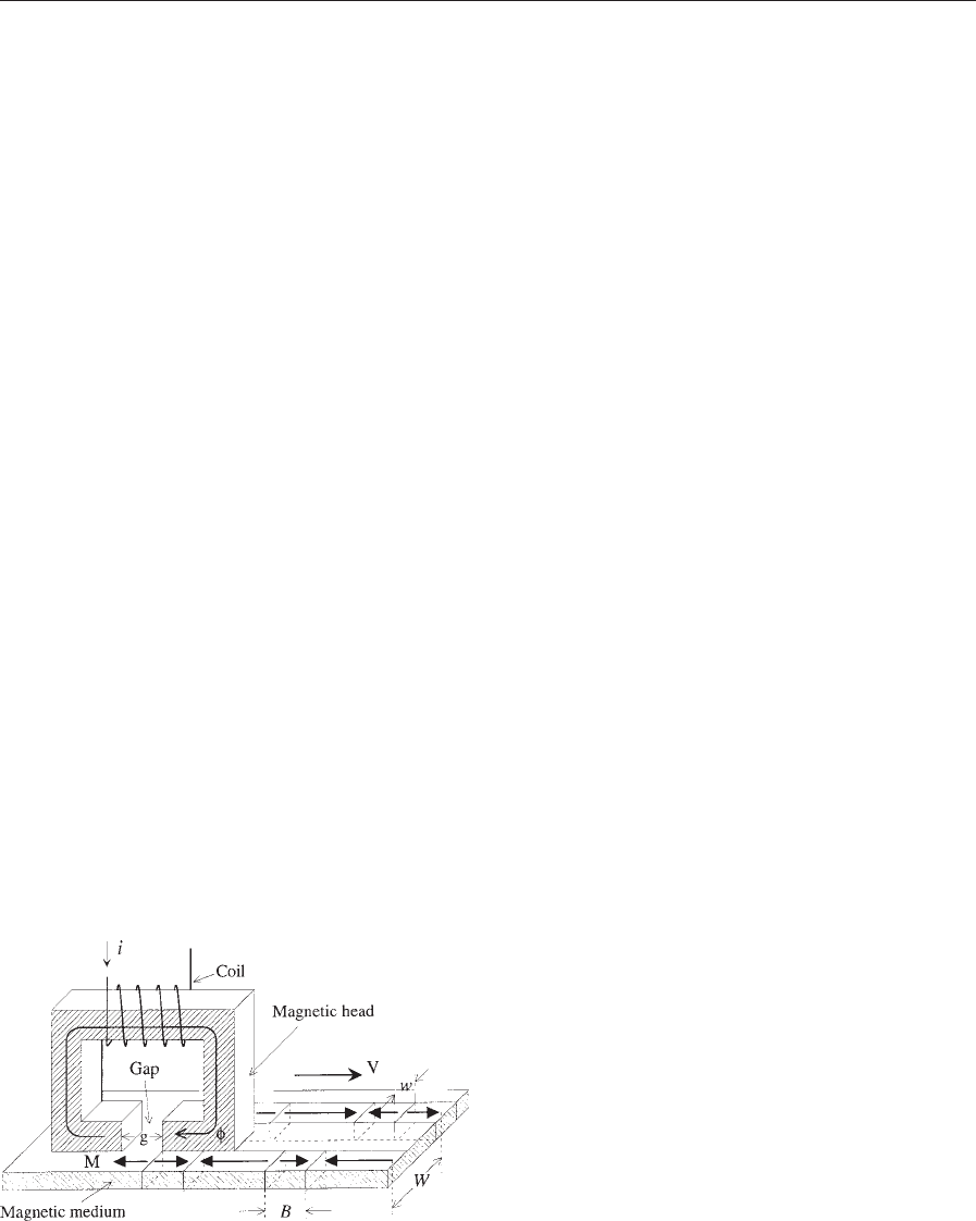
and low cost. In its simplest form, a magnetic re-
cording system consists of a magnetic head and a
magnetic medium, as schematically shown in Fig. 1.
The head is made of a piece of magnetic material in a
ring shape, with a small gap facing the medium and a
coil away from the medium.
The head records and reproduces information,
while the medium stores the information. The re-
cording process is based on the phenomenon that an
electric current i generates a magnetic flux j as de-
scribed by Ampere’s law. The flux j leaks out of the
head core at the gap, and magnetizes the magnetic
medium. The orientation of the magnetization is de-
termined by the current direction. As the medium
moves from left to right with a velocity V under the
head gap, magnetization is retained in the medium at
different locations.
There are two types of head used in reproducing.
One senses magnetic flux change rate, and the other
senses the magnetic flux. During the reproduction
process, a magnetized medium is placed under the
head gap. A part of the flux coming out of the me-
dium surface enters the head through the gap. As
the medium moves, the prerecorded information is
reproduced by the head.
The distance between two closest transitions in the
medium is the flux change length B, and the distance
between two adjacent data tracks is the track pitch
W, which is wider than the data track width w. The
flux change length can be directly converted into bit
length with the proper coding scheme. The recipro-
cals of the bit length and the track pitch are termed
the linear density and the track density, respectively.
Their product yields the areal density of the infor-
mation stored in the medium. This areal density is a
figure of merit for a recording system.
The research and development efforts of the mag-
netic recording industry have been focused on in-
creasing the areal density. During the 1990s, the areal
density was increasing at 60% annual rate. More re-
cently, the rate has been accelerated to more than
100%. At present, hard disk drives used in desktop
computers feature areal densities of more than
30 Mb mm
2
(Bo0.06 mm and Wo0.6 mm). This
yields a total storage capacity of more than 30 Gb
for a disk of 95 mm diameter.
1. Magnetic Media and Magnetic Heads
Magnetism is the result of uncompensated electron
spin motions in an atom. Only transition elements
exhibit this property, and nearly all practical interest
in magnetism centers on the first transition group of
elements (manganese, iron, nickel, and cobalt) and
the rare earth elements (gadolinium, and terbium).
While the first transition group of elements and their
alloys are the materials used in magnetic recording,
amorphous rare earth-transition metal alloys are the
only commercially used magneto-optical storage me-
dium. The strength of magnetism is represented by
magnetization M, and is related to magnetic field H
and magnetic flux density B by
B ¼ m
0
ðH þ MÞð1Þ
where m
0
is the permeability of vacuum. The ratio of
B with and without a magnetic material is the relative
permeability m of that magnetic material.
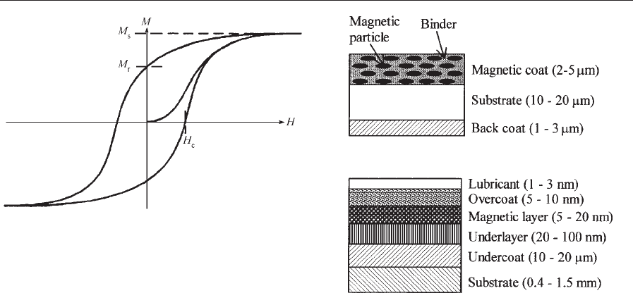
When a magnetic field H is applied to a piece of
demagnetized magnetic material, the magnetization
M starts increasing with H from zero. The rate of
increase gradually slows down and M asymptotically
approaches a value M
s
.IfH is reduced to zero, M
follows to a lower value M
r
. Further reduction of H
to a very high negative value will magnetize the ma-
terial to M
s
. In order to bring the material to the
demagnetized state, a positive field H
c
is required.
Continuous increase in H field will bring the trace of
M to a closed loop. This loop is the major hysteresis
loop, as illustrated in Fig. 2.
The hysteresis loop shows that magnetic material
has memory. It is this memory that is used in the
medium for storing information. H
c
is the coercivity,
indicating the strength of magnetic field required to
erase the memory of a magnetic material. Magnetic
materials with high H
c
are ‘‘hard’’ magnets, and are
Figure 1
Conceptual diagram of a magnetic medium and an
inductive head.
627
Magnetic Reco rding Technologies: Overview
suitable for recording media applications if they also
have high M
r
. On the other hand, magnetic materials
with low H
c
are ‘‘soft’’ magnets, and are candidates
for head core materials if they also have high M
s
and
high m. M
r
and M
s
are the remanent and saturation
magnetization, respectively, and their ratio is the
remanent squareness.
There are two groups of magnetic media. The first
group is called particulate media because the mag-
netic materials are in the form of particles. This group
includes oxide (g-Fe
2
O
3
), cobalt-modified iron oxide
(g-Fe
2
O
3
þCo), metal particles, and barium ferrite
(BaFe
12
O
19
). Some of these have been used in mag-
netic recording for several decades. The other group
of media is called the thin-film media, because the
magnetic layer can be deposited as a continuous thin
film. Most materials in this group are cobalt-based
alloys. Compared with particulate media, the thin-
film media usually have a higher coercivity H
c
and a
higher remanence M
r
, and are suitable for high areal
density applications.
Magnetic media can be classified into three general
forms of applications. Tape is the oldest form and
remains an important medium today. It is central to
most audio, video, and instrumentation recording,
although it is also used in the computer industry for
archival storage. It is economical and has a large ca-
pacity, but suffers slow access time. Hard disk is tra-
ditionally the primary storage unit inside a computer,
and is just being introduced in the consumer market
(audio/video box). It provides the user with fast data
access, but has poor transportability. Flexible disk is
designed for easy data removability, but is limited in
capacity. Besides these three general forms of appli-
cations, a hybrid of flexible medium and hard disk
has appeared recently. It is a removable rigid disk
capable of holding up to several gigabytes of digital
data. In addition, magnetic stripes are getting widely
used in various forms of cards.
The magnetic layer alone cannot be used as a me-
dium. It needs additional components to improve its
chemical and mechanical durability. Typical cross
sections of a particulate magnetic tape and a thin-film
hard disk are shown in Fig. 3. In the case of tape
application, iron particles with a typical size of 0.5 mm
long and 0.1 mm wide are dispersed in a polymeric
binder, together with solvents, lubricants, and other
fillers to improve magnetic and mechanical durability.
This dispersed material is then coated on a biaxially
oriented polyethylene terephthalate substrate. An op-
tional back coat may also be applied to the other side
of the substrate. The cross section of a hard disk is
more complex. A high-purity aluminum–magnesium
(5 wt.%) substrate is diamond-turned to a fine surface
finish, and then electrolessly plated with a nonmag-
netic nickel–phosphorus (10 at.%) undercoat.
This layer is used to increase the hardness, reduce
the defects, and improve the finish of the aluminum–
magnesium alloy, and is polished to a super surface
finish. Next, an underlayer of chromium is sputtered
to control the properties of the magnetic film, fol-
lowed by sputtering the magnetic film. Finally, a layer
of hydrogenated or nitrogenated carbon is over-
coated on the magnetic film, and an ultrathin layer of
perfluorinated hydrocarbon liquid lubricate is ap-
plied on top. The carbon and lubricant layers are
used to improve the corrosion and mechanical resist-
ance of the disk. To achieve high shock resistance,
glass disk is sometimes used, especially in mobile ap-
plications. For a 95 mm disk, the finished product
should have a surface flatness better than 8 mm and an
arithmetic average roughness (R
a
) of less than 0.3 nm.
Magnetic heads serve three functions: recording,
reproducing, and erasing. Two groups of head are
employed to carry out these three functions. The
Figure 2
Hysteresis loop of a magnetic material.
Figure 3
Cross-sections of a particulate magnetic tape (top) and a
thin-film hard disk (bottom).
628
Magnetic Reco rding Technologies: Overview
first group is the inductive heads, as schematically
illustrated in Fig. 1. The evolution of the inductive
head follows the selection of core materials, as shown
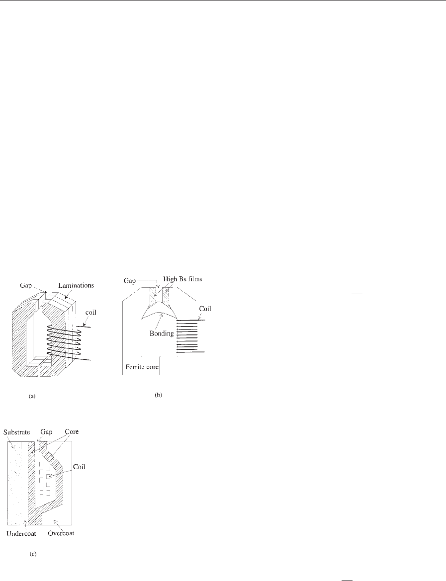
in Fig. 4. Early heads used laminated molybdenum
Permalloy (Ni–Fe–Mo, 79–17–4 wt. %). The primary
drawbacks are frequency limitation, gap dimension
inaccuracy, mechanical softness, and frequency lim-
itation caused by eddy current loss. One way to re-
duce eddy current loss is to increase core material
electric resistivity. Two types of ferrite material have
high resistivity (four to nine orders higher than Perm-
alloy) and reasonable magnetic properties: nickel–
zinc and manganese–zinc.
These materials are also very hard, providing great-
er head durability during head/medium contacts. The
major deficiency of ferrite materials is their low B
s
values. In order to record in high H
c
media, high flux
density B is needed in the head core. When the flux
density in the core material reaches its saturation B
s
,it
will not increase despite the increase of recording cur-
rent or coil turns. This saturation starts from the cor-
ners of the gap due to its geometry. To remedy this
deficiency, a layer of metallic alloy material with much
higher B
s
is deposited on the gap faces. This type of
head is called the metal-in-gap (MIG) head.
Thin-film heads capitalize on semiconductor-like
processing technology to reduce the customized fab-
rication steps for individual heads. The core, coil, gap,
and insulator layers are all fabricated by electroplat-
ing, sputtering, or evaporation. Due to the nature of
the semiconductor process, the fabrication is more
accurate for small dimensions. Small gap dimensions
are suitable for high linear and track density, and
small core dimensions allow the use of high B
s
Perm-
alloy material (nickel–iron, 80–20 wt. %) as a core
with low inductance for high data-rate applications.
The high cost of the semiconductor-like process is
offset by high throughput: a 150 mm 150 mm wafer
can produce 40 000 pico-slider heads (1.25 1.00
0.30 mm). One disadvantage is the limited band-
recording capability because the small pole length
limits low-frequency response. A second disadvantage
is the Barkhausen noise, which is characterized as the
sudden jump of magnetic flux flowing around the
head, and is caused by the relatively small number of
magnetic domains in the core.
The recording and erasing functions are performed
by an inductive head in all magnetic recording devices.
The reproducing function, however, can be carried out
either by an inductive head or by a magnetoresistive
(MR) head. The reproducing performance of an in-
ductive head is described by Faraday’s equation:
v ¼nV
df
dx
ð2Þ
where v is the output electric voltage from the head, n
is the number of the coil turns, V is the medium mov-
ing velocity, and dj/dx is the derivative of the mag-
netic flux with respect to medium moving direction.
When an inductive head is used for reproducing,
this head is usually also used for recording and eras-
ing. The optimal performance cannot be achieved
because recording and reproducing have contradic-
tory requirements for head design. To solve this
problem, a new reproduction head was introduced in
the 1990s. This is the MR head. An MR head is al-
ways integrated together with an inductive head in
such a way that the MR head performs the repro-
ducing and the inductive head carries out the record-
ing and erasing.
The first generation of MR head introduced in
1990 is the anisotropic type (AMR). As shown in
Fig. 5, conceptually, an AMR head has a magneto-
resistive element (MRE) and two electric leads. The
MRE is a Permalloy stripe (nickel–iron, 80–20 wt.%),
with thickness t, width w, and height h. An electric
current, with density J, passes through the MRE
through the leads. The electric resistivity of the
MRE is a function of the angle y between J and MRE
magnetization M:
r
y
¼ r 1 þ
Dr
r
cos
2
y
ð3Þ
Figure 4
Various inductive head structures: (a) laminated, (b)
MIG, and (c) thin film.
629
Magnetic Reco rding Technologies: Overview