Buschow K.H.J. (Ed.) Concise Encyclopedia of Magnetic and Superconducting Materials
Подождите немного. Документ загружается.

crystallographic c axis) it is strongly reduced. The
corresponding resistivity values are referred to as
r
ab
and r
c
, respectively. Near room temperature for
a typical cuprate such as YBa
2
Cu
3
O
7d
we have
the values r
ab
¼200–500 mOcm, compared to r ¼2–
5 mOcm for a typical metal. The ratio r
c
/r
ab
of the
anisotropy near room temperature ranges from 30–60
for YBa
2
Cu
3
O
7d
up to 1 10
5
for Bi
2
Sr
2
CaCu
2
O
8
.
The fact, that near room temperature r
ab
is about 100
times larger than the resistivity in a typical metal, is
partly due to the lower charge carrier concentration
and the pronounced anisotropy in the cuprate.
Above the critical temperature T
c
near optimum
doping the normal-state resistivity of many cuprate
superconductors increases linearly with temperature.
A prominent exception is the electron-doped cuprate
Nd
2x
Ce
x
CuO
y
showing r
ab
BT
2
near optimum dop-
ing. This normal-state resistive behavior can be qual-
itatively explained in terms of the nature of the
scattering processes and the electronic density of
states (DOS). It is now well established that in the
cuprates the electron scattering processes are domi-
nated by the electron–electron interaction, in contrast
to electron–phonon scattering prevailing in metals.
An important piece of evidence for this scattering
behavior comes from the pronounced increase of the
electron mean free path with decreasing temperature
below T
c
as soon as the quasi-particles (as scattering
partners) are frozen out because of the opening of the
energy gap. With decreasing temperature this also
leads to a sharp upwards turn of the thermal con-
ductivity k(T)atT
c
. The thermal conductivity then
passes through a maximum near T
c
/2. If the electron–
phonon interaction would dominate, such an abrupt
change of the temperature dependence of the electron
mean free path at T
c
would not be expected.
The r
ab
BT
2
behavior observed near optimum
doping in Nd
2x
Ce
x
CuO
y
is well consistent with the
electron–electron interaction as the dominant scat-
tering mechanism. On the other hand, the linear tem-
perature dependence r
ab
BT found usually in the
optimally hole-doped cuprates can be qualitatively
explained by a sharp peak (Van Hove singularity) in
the electronic DOS near the Fermi energy E
F
. The
additional phase space for scattering within this peak
region then leads to the proportionality for the scat-
tering rate t
1
Bk
B
T (marginal Fermi liquid), instead
of the usual Fermi liquid behavior t
1
B(k
B
T )
2
.
Here, k
B
is Boltzmann’s constant (Newns et al. 1993).
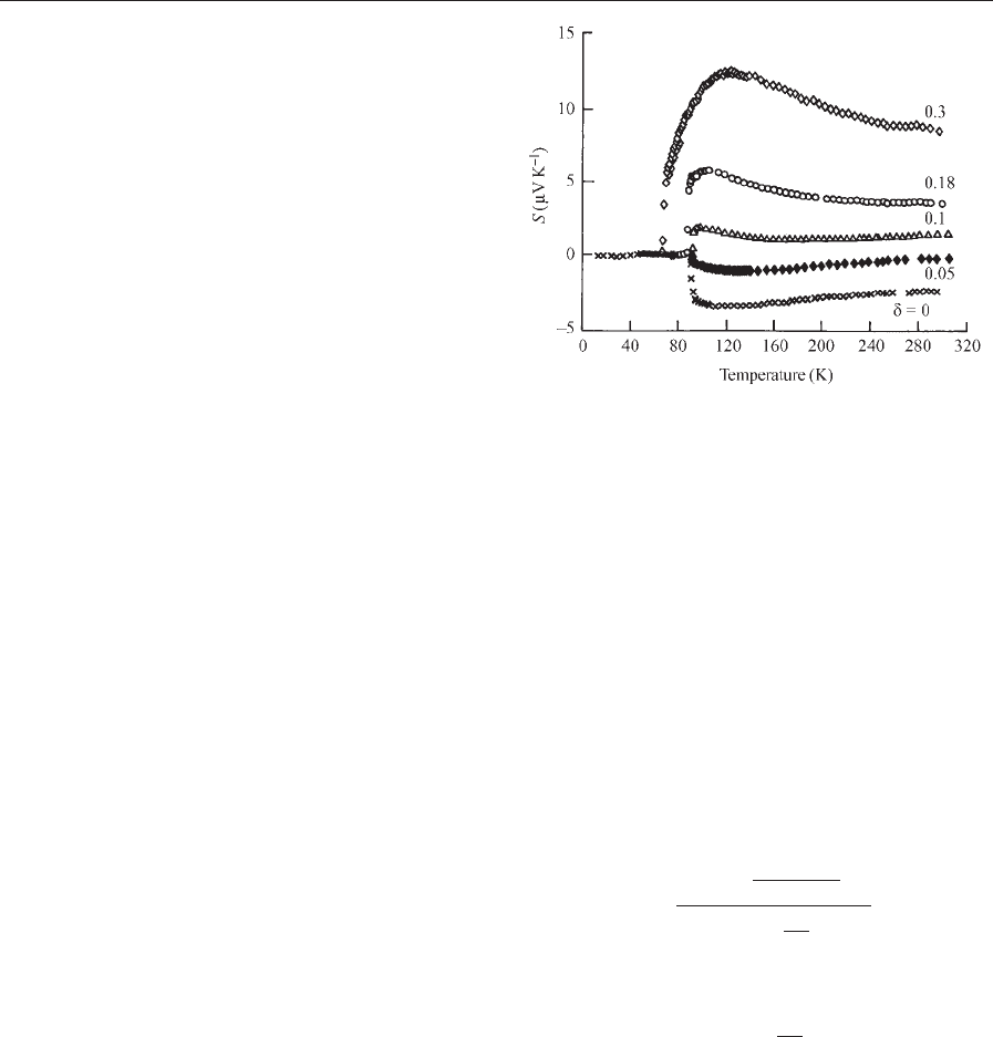
The normal-state thermopower (Seebeck coeffi-
cient) represents a transport property depending
highly sensitively on the electronic structure and the
doping level of the cuprates. There exists an interest-
ing correlation between the thermopower and the
critical temperature T
c
. Depending on the doping
level, the thermopower at room temperature of dif-
ferent p doped systems follows a universal curve tra-
versing zero at optimum doping (corresponding to
the maximum value of T
c
). The typical temperature
dependence of the thermopower shows an increase of
its absolute value above T
c
, turning into a flat curve
with falling tendency at higher temperatures. This
behavior is strongly different from the proportion-
ality to T expected in the limit of a wide (bk
B
T)
conduction band. A typical series of curves is shown
in Fig. 1 for YBa
2
Cu
3
O
7d
at different levels d of
oxygen depletion (Cooper et al. 1991).
This dependence of the thermopower on the tem-
perature and the doping level can be understood from
standard transport theory in combination with the
sharp peak in the electronic DOS near the Fermi
level. For the (positive) holes the thermopower is
S ¼
k
B
7e7
Z
s
E
@f
@E
E E
F
k
B
T
dE
Z
s
E
@f
@E
dE
ð1Þ
with the electric conductivity given by
s ¼
Z
s
E
@f
@E
dE ð2Þ
(Kubo–Greenwood formula). Here f is the Fermi
function, and s
E
contains the density of states and the
scattering processes. We emphasize that, because of
the sharp peak in the electronic DOS near E
F
, the
derivative @f/@E changes only little in the relevant
energy interval. From Eqn. (1) we can predict the
following qualitative behavior.
If E
F
is smaller (larger) than the energy of the DOS
peak, the contribution with EE
F
40(o0) domi-
nates and the thermopower will be positive (nega-
tive). Hence, the sign reversal of the thermopower is
Figure 1
Thermopower S of the cuprate YBa
2
Cu
3
O
7d
versus
temperature for different values d of the oxygen
depletion (after Cooper et al. 1991).
310
High-temperature Superconductors: Transport Phenomena

expected, when the Fermi energy coincides with the
energy of the DOS peak. Alternatively, according to
the ‘‘Van Hove scenario’’ of high-temperature super-
conductivity this location of the Fermi level corre-
sponds exactly to the optimum doping level yielding
the maximum value of T
c
. The experiments per-
formed with different p doped cuprate systems at
varying doping levels mentioned above well con-
firmed these ideas (Newns et al. 1993).
In the orthorhombic form of the cuprate
YBa
2
Cu
3
O
7d
one of the copper oxide planes per el-
ementary cell contains CuO chains along the b axis,
but not along the a axis. This introduces some an-
isotropy of the transport properties even within the
ab planes, in addition to the large anisotropy between
the ab plane and the c direction.
The normal state Hall effect represents a compli-
cated subject. However, it is this effect that led to
the concepts of ‘‘hole-doped’’ and ‘‘electron-doped’’
cuprate superconductors. The Hall coefficient R
H
¼
1/nq yields information on the nature of the charge
carriers involved in the electronic transport. Here n
and q are the concentration and elementary charge of
the charge carriers, respectively. For hole-doped con-
ductors R
H
is positive, whereas for electron-doped
materials it is negative. For the magnetic field orien-
tation in c direction in most of the high-temperature
superconductors R
H
is positive, indicating hole dop-
ing. Compounds derived from Nd
2
CuO
4
by substitu-
tional alloying (Nd
2x
Ce
x
CuO
y
) are the major
exception and show electron doping. In the latter
case of Nd
2x
Ce
x
CuO
y
an additional complication
arises from the fact that a two-band model appears to
be necessary, with an electron-like and a hole-like
section, for describing the electronic properties.
An unexpected result of the Hall effect measure-
ments is the observed strong temperature dependence
of the Hall coefficient, especially near optimum dop-
ing. Such a temperature dependence does not arise in
a canonical Fermi liquid. In YBa
2
Cu
3
O
7
, the most
intensively studied cuprate superconductor, for the
inverse Hall coefficient the relation R
1
H
¼a þbT has
been found, where a and b are constants. An inter-
esting quantity is the Hall angle, y
H
, the angle
between the electric current density and the total
electric field, which is given by tany
H
¼R
H
B/r. From
electronic transport theory, one finds that tany
H
is
equal to /o
c
tS, a weighted average for the dominant
conducting particles of the product of their cyclo-
tron frequency o
c
¼qB/m* for the electron orbits
in the magnetic field and their scattering time t (m* ¼
effective mass).
Hence, coty
H
is expected to be proportional to the
scattering rate t
1
. In YBa
2
Cu
3
O
7d
across the whole
of the metallic doping range the relation co-
ty
H
¼a þbT
2
is valid in good approximation, again,
a and b being constants. We conclude that the scat-
tering rate also shows this a þbT
2
temperature de-
pendence. Noting R
1
H
Bn and rB(nt)
1
, we see that
the linear temperature dependence of R
1
H
and the
(a þbT
2
) behavior of the scattering rate appear con-
sistent with the linear temperature dependence of the
resistance observed in many cuprates discussed
above. We emphasize that we must restrict our dis-
cussion to rough and qualitative remarks only, leav-
ing out many details of the electronic structure of
these materials.
2. Granular Structure
Except for the highly specialized procedures for ma-
terial fabrication developed for the growth of axis-
oriented epitaxial films and single crystals, the high-
temperature superconductors are usually prepared as
ceramics with a granular structure. Within the grain
boundary regions superconductivity is strongly weak-
ened or even totally absent. Hence, the grain bound-
aries in the cuprate superconductors have to date
presented a challenging technological problem. It still
is an important goal of the present technological de-
velopments to minimize the residual electric resist-
ance due to the grain boundaries as much as possible.
Recently, special doping processes for the grain
boundaries in order to improve the electric conduc-
tivity in these regions have been discussed. The im-
portant quantity to deal with is the critical current
density at which a specific nonzero electric field is
generated in the superconductor, resulting in power
dissipation. The current flow pattern in a multigran-
ular superconductor has been treated in analogy to
the structure of a brick wall (brick wall model). In
addition to the granular structure, the poor ductility
of the cuprate superconductors continues to represent
a severe obstacle, in particular for the technological
power applications.
For the applications of high-temperature super-
conductors in microelectronics the critical current
density in thin films has received a large amount
of attention. Here c axis oriented epitaxial films of
YBa
2
Cu
3
O
7d
clearly represent the work horse. At
77 K and in zero magnetic field, critical current den-
sities of 1 10
6
–1 10
7
Acm
2
have been achieved, a
highly impressive result of the associated materials
science.
Whereas the grain boundaries in the cuprate su-
perconductors are clearly detrimental to many tech-
nical applications, in one specific case they turned out
to be extremely useful and they represent a well con-
trollable and stable Josephson junction. The grain
boundary Josephson junctions are fabricated by
growing an epitaxial superconducting cuprate film
on a bicrystal acting as the substrate. The grain
boundary separating the two single-crystalline pieces
of the substrate is then transferred to the epitaxial film
deposited subsequently on the bicrystalline substrate.
In this way, during recent years Josephson devices and
superconducting quantum interferometers (SQUIDs)
311
High-temperature Superconductors: Transport Phenomena

operating up to 77 K have been fabricated (see
Josephson Junctions: High-T
c
).
3. Current-induced Vortex Motion
In a magnetic field in the range between the lower and
upper critical field, B
c1
and B
c2
, respectively, below
the critical temperature T
c
the superconducting
mixed state is established. In the mixed state the su-
perconductor is penetrated by a more or less perfectly
ordered 2D lattice of flux lines, each flux line carrying
a single magnetic flux quantum j
0
. The regularity of
this lattice depends on the spatial homogeneity of the
superconductor. The following will be restricted to
the case where the magnetic field and, hence, the flux
lines, are oriented along the crystallographic c axis. In
this case the flux lines degenerate into stacks of pan-
cake vortices (or point vortices) attached to the CuO
2
planes constituting the superconducting structural el-
ements of the cuprates. Under the influence of an
external force the flux lines or pancake vortices can
be set into motion. This vortex motion represents one
of the most important processes in superconductors,
since it results in an electric field of quantum me-
chanical origin and thereby destroys superconductiv-
ity (Huebener 2001).
An electric transport current of density
j generates
the Lorentz force
j j
0
per unit length of flux line.
The dynamic state of the vortex lattice is determined
by the force equation:
j j
0
Zv
j
aðv
j
nÞþf
p
¼ 0 ð3Þ
The Lorentz force is balanced by the damping force
Z
v
j
, the Hall force aðv
j
nÞ, and the pinning force
f
p
v
j
is the vortex velocity, Z and a are damping
coefficients,
n is a unit vector in magnetic field direc-
tion. Vortex motion always results in an electric field
E according to the equation:
E ¼v
j
B ð4Þ
Equation (4) is derived from the phase change of
the macroscopic wave function describing the Cooper
pair condensate, effected by the vortex motion. (It is
intimately connected with the Josephson voltage fre-
quency relation.) In the absence of the Hall force and
the pinning force we see from Eqns. (3) and (4) that
n
j
is perpendicular to j and, therefore, E is parallel to
j. As a result power dissipation E j per unit volume
occurs, and superconductivity is destroyed. It is this
mechanism of current induced vortex motion and the
appearance of flux-flow resistance which represent
the main challenge to maintaining superconductivity.
Because of the three characteristic novel features of
the high-temperature superconductors (high critical
temperature, small coherence length, and large an-
isotropy) vortex motion and the appearance of flux-
flow resistance is highly facilitated in the cuprates and
turns out to be an even more challenging issue than in
the classical superconductors.
It is the pinning force in Eqn. (3) which can result
in a strong reduction of vortex motion and, hence,
contributes to sustaining superconductivity at finite
electric transport current. Flux pinning is accom-
plished by material inhomogeneities (pinning centers)
causing a local depression of the Gibbs free energy
density of the vortex lattice. Because of the short co-
herence length in the cuprates, atomic size defects,
such as oxygen vacancies in the CuO
2
planes or de-
fects produced by substitutional alloying, already act
as important pinning centers. The pinning force even-
tually acting on the vortex lattice results from the
combination of the elementary pinning interaction
between a vortex and the pinning center with the
elastic properties of the vortex lattice. The elastic
properties come in, since the vortex lattice must be
deformed in order to accommodate the spatial con-
figuration of the pinning sites. Because of this, flux
pinning turns out to be a highly complex phenome-
non. However, because of its extreme importance for
the technical applications of the cuprate supercon-
ductors, the subject of flux pinning has recently at-
tracted a large amount of research and development.
If the damping force Z
n
j
and the pinning force
would be absent in Eqn. (3), the vortices would move
parallel to the current density
j, the electric field E
would be perpendicular to
j (pure Hall electric field),
and the power dissipation
j E would vanish. How-
ever, for this to happen the quasi-particle scattering
time t must approach the limit t-N.
According to the Bardeen–Stephen model, valid
for the classical superconductors and serving, at best,
as a qualitative orientation for the high-temperature
superconductors, the flux-flow resistivity r
f
is given
by
r
f
¼ r
n
B
B
c2
where r
n
is the normal-state resistivity. In this model
the vortex core is taken as a normal-state cylinder of
radius x. The ratio B/B
c2
then represents the volume
fraction of this normal phase. For the damping co-
efficient Z one finds Z ¼j
0
B
c2
/r
n
. In the current-in-
duced flux-flow state the Hall angle y
H
is given by tan
y
H
¼o
c
t, similar to the situation in the normal
state. In the superconducting mixed state of the
cuprates the Hall angle is generally small (typically
tan y
H
E1 10
2
), and dissipative vortex motion
perpendicular to the electric current direction
dominates.
In contrast to the classical superconductors, in the
cuprate superconductors the description of the vortex
core as a normal-state cylinder of radius x is only a
rough approximation. Here also the symmetry of the
pair wave function must be discussed. It is now well
established that in the p-doped cuprates the pair wave
312
High-temperature Superconductors: Transport Phenomena
function shows d-wave symmetry, with four node
lines where the gap energy reaches zero. This has im-
portant consequences for the quasi-particle scattering
in the mixed state. However, at present the experi-
mental and theoretical clarification of this point is
still in progress. Another new aspect of quasi-particle
scattering originates from the extremely short coher-
ence length and the corresponding small vortex-core
diameter in the cuprates. As a result, quantum effects
of the electronic structure of the vortex cores (quan-
tum confinement) can become important. The de-
scription of the vortex core as a normal-state cylinder
of radius x is then highly inadequate. At least in the
limit T5T
c
this can lead to a strong reduction of the
phase space available for quasi-particle scattering.
Again, at present this issue is still under experimental
and theoretical investigation (Huebener 2001).
The peculiar features of the high-temperature
superconductors (high critical temperature, short
coherence length, and anisotropy leading to the pan-
cake-vortex structure) have important consequences
for the dynamic properties of the vortex lattice. There
exists an irreversibility line in the phase space of
magnetic field and temperature, above which the
magnetization is perfectly reversible with no detect-
able flux pinning. Alternatively, below this line the
magnetization becomes hysteretic, and the equilibri-
um vortex distribution cannot be established any
more because of flux pinning. From these observa-
tions in the 1990s the new concept of ‘‘vortex matter’’
evolved, with a liquid, glassy, and crystalline state,
displaying a complex phase diagram. These novel
features strongly influence the transport processes
associated with vortex motion.
An immediate result of the different phases of vor-
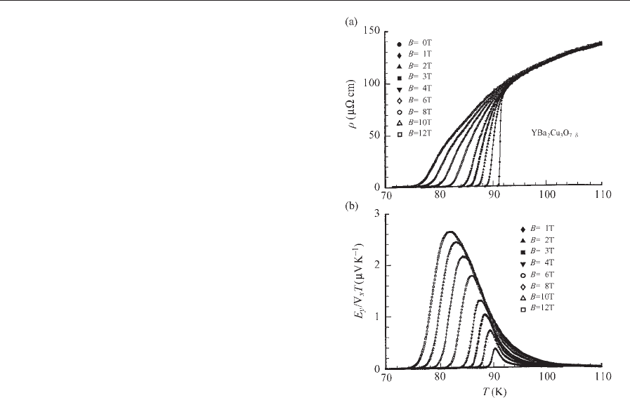
tex matter appearing in the mixed state is the broad-
ening of the resistive transition in a magnetic field.
Whereas in the classical superconductors the drop in
the electric resistivity due to the onset of supercon-
ductivity is usually shifted to lower temperatures with
increasing magnetic field, in high-temperature super-
conductors the resistively measured onset tempera-
ture of superconductivity is only weakly magnetic
field dependent, but the transition curve is broadened
instead, and the broadening increases strongly with
increasing magnetic field. A typical case is shown in
Fig. 2a for an epitaxial c axis oriented YBa
2
Cu
3
O
7d
film for magnetic fields ranging from 0 to 12 T and
oriented in c direction. An exception from this broad-
ening of the resistive transition in a magnetic field has
been observed for the electron-doped cuprate super-
conductor Nd
2x
Ce
x
CuO
47y
in the whole doping re-
gime from slightly underdoped to slightly overdoped.
Here the whole resistive transition curve is shifted to
lower temperatures with increasing magnetic field,
more like in classical superconductors.
The motion of the vortex lattice due to the Lorentz
force of an electric transport current is accompa-
nied by the transport of entropy carried by the vortex
lattice. This entropy transport causes a temperature
gradient perpendicular to the directions of the electric
current and magnetic field. It is referred to as the
Ettinghausen effect and has been observed in a
number of high-temperature superconductors. If the
electric current density j
x
is assumed in x direction
and the magnetic flux density B
z
in z direction, the
heat current density U
y
in y direction associated with
the entropy transport is
U
y
¼ eB
z
kj
x
ð5Þ
Here e is the Ettinghausen coefficient and k the heat
conductivity. The Ettinghausen effect represents one
of the major observations supporting the concept of
vortex motion as the mechanism generating the elec-
tric resistance in the superconducting mixed state.
The experiments on the flux-flow Hall effect in the
cuprate superconductors indicated an unexpected re-
versal of the sign of the Hall voltage at temperatures
below the superconducting transition. This effect has
been observed in different materials and appears to
Figure 2
(a) Flux-flow resistivity of the cuprate superconductor
YBa
2
Cu
3
O
7d
versus temperature for different magnetic
fields oriented in c direction. (b) Normalized Nernst
electric field E
y
/r
x
T versus temperature for the same
sample and magnetic fields as in (a).
313
High-temperature Superconductors: Transport Phenomena
represent an intrinsic property. A satisfactory theo-
retical understanding of this effect has not yet been
reached, and the theoretical discussions are still con-
troversial.
4. Vortex Moti on in a Temperature Gradient
In a temperature gradient applied to a superconduc-
tor in the mixed state the thermal force S
j
gradT
acts on the vortex structure, driving the magnetic flux
quanta from the hot to the cold side of the specimen.
Here S
j
is the transport entropy per unit length of
flux line. The thermal force is the driving force in all
thermal diffusion phenomena, and the transport en-
tropy represents a characteristic property of the spe-
cific type of particle under consideration. (The heat
current density U carried by a flux-line lattice moving
with velocity
v
j
is U ¼nTS
j
v
j
, where n ¼B/j
0
is the
density of flux lines.) For treating the dynamic state
of the vortex lattice driven by a temperature gradient,
in Eqn. (3) the Lorentz force
j j
0
must be replaced
by the thermal force S
j
gradT. If we neglect the Hall
effect and flux pinning, take the temperature gradient
in x direction and the magnetic field in z direction, we
see from Eqn. (4) that the resulting flux-flow electric
field is oriented in y direction. This electric field E
y
is
given by
E
y
¼ nB
z
@T
@x
ð6Þ
and the effect is referred to as the Nernst effect. n is
the Nernst coefficient. The Ettinghausen coefficient e
and the Nernst coefficient n are coupled through the
Bridgman relation of irreversible thermodynamics
Tn ¼ ek ð7Þ
The Nernst effect has been investigated in the mixed
state of a number of high-temperature superconduc-
tors. In Fig. 2(b) we show typical results obtained for
the same epitaxial YBa
2
Cu
3
O
7d
film and the same
magnetic fields as in Fig. 2(a). In the normal state
sufficiently far above T
c
(of about 91 K in this case)
the Nernst electric field E
y
is seen to be negligible.
With decreasing temperature E
y
increases and passes
through a maximum. As one expects because of the
flux-flow process, E
y
increases with increasing flux
density B. On the low-temperature end of the curves
the Nernst electric field E
y
and the resistivity vanish
because of flux pinning. From Fig. 2(b) we see also,
that the flux-flow Nernst effect clearly extends to
temperatures well above the critical temperature T
c
measured at zero magnetic field.
This is due to fluctuation effects, which become
stronger with increasing magnetic field. These fluctu-
ation effects can be measured with high accuracy,
since the Nernst effect is negligible in the normal state,
and a special subtraction procedure is not necessary.
Because of the small coherence length, high critical
temperature, and large anisotropy in the cuprate, su-
perconductor fluctuations play a much more promi-
nent role than in the classical superconductors. Hence,
this subject has received much experimental and the-
oretical attention.
In thermal diffusion experiments the high sensiti-
vity of the properties of a superconductor to the
temperature represents an important point, and
the application of a large temperature gradient to
the sample often causes complications. However, an
interesting exception is a geometry, where the sample
dimension in the direction of the temperature gradi-
ent is kept small, e.g., about 100 mm. In this case a
large temperature gradient can be achieved even for a
small temperature difference between the hot and the
cold side of the sample.
In our discussion of the thermal diffusion of mag-
netic flux quanta we have neglected the Hall force
að
n
j
nÞ. However, if we include the latter force, a
finite Hall angle of the resulting vortex velocity
n
j
appears, generating a component n
jy
perpendicular
to the direction of the temperature gradient. This ve-
locity component n
jy
produces a longitudinal electric
field component E
x
, i.e., a contribution to the See-
beck effect. Furthermore, in the superconducting
mixed state the responses of the quasi-particles to the
applied temperature gradient also must be discussed,
in addition to that of the magnetic flux quanta.
However, this subject is beyond the scope of this ar-
ticle, and we refer to the treatments by Huebener
(1995, 2001).
5. Concluding Remarks
Since their discovery in 1986 the cuprate supercon-
ductors have attracted a large amount of research
and engineering developments worldwide. One of the
main reasons for this strong interest has been the fact
that in many cuprates the critical temperature of su-
perconductivity is well above the boiling point of
liquid nitrogen. The layered crystallographic struc-
ture of these materials with the CuO
2
planes repre-
sents the most prominent characteristic feature
dominating the electronic properties. The undoped
cuprate perovskites are antiferromagnetic electric in-
sulators and become electric conductors and super-
conductors only by doping. Most high-temperature
superconductors are p doped, but n doping also leads
to superconductivity in some cases. While supercon-
ductivity is based on Cooper pairs as in the classical
superconductors, the pairing mechanism still remains
unclear.
It is now well established that in the hole-doped
cuprates the pair wave function shows d-wave sym-
metry, whereas the symmetry is not yet as clearly
known in the electron-doped cuprates. In many ways
the normal-state electronic transport properties do
314
High-temperature Superconductors: Transport Phenomena

not show the canonical Fermi liquid behavior well
known for metallic conductors. However, these prop-
erties of the normal state continue to provide clues
regarding the superconducting pairing mechanism.
The critical temperature value of many high-temper-
ature superconductors above the boiling point of liq-
uid nitrogen clearly represents an important asset for
practical applications. However, the granular struc-
ture and poor ductility still provides a challenge for a
technology based on these materials.
See also: Electrodynamics of Superconductors: Flux
Properties; Superconducting Thin Films: Multilayers;
High-temperature Superconductors: Thin Films and
Multilayers
Bibliography
Bednorz J G, Mu
¨
ller K A 1988 Perovskite-type oxides—the new
approach to high-T
c
superconductivity. Rev. Mod. Phys. 60,
585–600
Cooper J R, Obertelli S D, Carrington A, Loram J W 1991
Effect of oxygen depletion on the transport properties of
YBa
2
Cu
3
O
7d
. Phys. Rev. B. 44, 12086–9
Huebener R P 1995 Superconductors in a temperature gradient.
Supercond. Sci. Technol. 8, 189–98
Huebener R P 2001 Magnetic Flux Structures in Superconduc-
tors. 2nd edn. Springer, Berlin
Levin K, Kim Ju H, Lu J P, Si Quimiao 1991 Normal state
properties in the cuprates and their Fermi liquid based in-
terpretation. Physica C 175, 449–522
Newns D M, Krishnamurthy H R, Pattnaik P C, Tsuei C C,
Chi C C, Kane C L 1993 Van Hove scenario for cuprate
superconductivity. Physica B 186–8, 801–7
Pickett W E 1989 Electronic structure of the high-temperature
oxide superconductors. Rev. Mod. Phys. 61, 433–512
Poole C P, Farach H A, Creswick R J 1995 Superconductivity.
Academic Press, San Diego, CA
Tinkham M 1996 Introduction to Superconductivity, 2nd edn.
McGraw-Hill, New York
Waldram J R 1996 Superconductivity of Metals and Cuprates.
Institute of Physics, Bristol, UK
R. P. Huebener
University of Tu
¨
bingen, Germany
315
High-temperature Superconductors: Transport Phenomena
This page intentionally left blank
316
Intermediate Valence Systems
The group of rare-earth elements comprise the series
from lanthanum (atomic number 57) to lutetium
(atomic number 71), where the electronic configura-
tion (EC) gradually changes from [Xe]4f
0
5d
1
6s
2
to
[Xe]4f
14
5d
1
6s
2
, respectively (see Localized 4f and 5f
Moments: Magnetism). Light elements of this series
like cerium, elements with a nearly half-filled 4f shell
like samarium and europium, or with an almost filled
4f shell like thulium and ytterbium may, however,
deviate from such a well-defined EC with integer
valency. As a result, the ions exhibit intermediate
valence (IV), representing a homogeneous quantum
mechanical mixture of two consecutive integer va-
lence configurations. Not only are rare-earth systems
known to show such valence instabilities, but about
40 elements (3d,4d,5d,5f ) and their compounds can
emerge in noninteger valency.
A necessary condition for nonintegral valence to
occur is that two bounding states of the rare earth,
i.e., 4f
n
(5d6s)
m
and 4f
n1
(5d6s)
m þ1
, are nearly de-
generate. The system may then lower its energy by
adopting a mixture of both EC and an additional
degree of freedom is acquired. On each 4f site charge
fluctuations appear between these configurations on a
typical time scale t
cf
. Experiments probing such sam-
ples on scales much shorter than t
cf
(like XPS) allow
it to observe both configurations, while experiments
with a much longer time scale (like Mo
¨
ssbauer effect)
reveal just the intermediate configuration. In these
systems, the 4f level is pinned to the Fermi energy E
F
,
provoking f electrons to escape into the conduction
band. Hence, the lifetime of the state becomes limited
and the former localized level acquires a narrow
width D with some dispersion and is, therefore, oc-
cupied by a nonintegral number of electrons. The
inverse of D is then given by t
cf
BD/_.
IV is derived from a quantum mechanical hybrid-
ization of two consecutive states a
n
7 f
n
S and a
n1
7
f
n1
S (Lawrence et al. 1981), which can no longer be
considered as a simple superposition. Rather, fluctu-
ations between both states modify physical properties
in a fundamental manner. Features like quenched
magnetic moments, an enhanced Pauli susceptibility,
and a large electronic contribution to the specific heat
may become obvious, which otherwise cannot be
found in both integer valent states involved.
Such homogeneously mixed systems are distin-
guished from the classical ‘‘mixed valence’’ phases like
Fe
3
O
4
or Sm
3
S
4
, where at crystallographic inequiva-
lent lattice sites the cations exhibit different oxidation
states with distinct electronic configurations.
A lattice-related aspect of IV materials is a soft
bulk modulus, indicating the large compressibility of
such systems (Wachter 1994). Since the ionic radius
of IV materials cannot be considered as a ‘‘hard
sphere’’ as for integral valent materials, pressure will
change the degree of IV and thus change the f oc-
cupation, which in turn is related to the ionic radius.
If a pressure induced transition towards an IV state
is of first order, the bulk modulus B
0
becomes infi-
nitely small, and as a consequence, the compressibi-
lity k1/B
0
diverges.
IV systems are also known for a negative elastic
constant c
12
which ensures (in the case of cubic crys-
tals) that even under applied uniaxial pressure the
crystal structure is preserved as it was firstly observed
in TmSe (Batlogg et al. 1979). The negative value of
c
12
also causes a negative Poison ratio c
12
/(c
11
þc
12
).
Measurements of the phonon dispersion relation in
IV materials show a common softening of the acous-
tic and the optical phonon branches when compared
to stable isostructural nonmagnetic systems. More-
over, well-defined crystal field (CF) splitting of the 4f
state has not been found in IV systems yet studied.
1. Some Theoret ical Aspects
The physics of intermediate valent materials is
usually accounted for in terms of the periodic (And-
erson model 1961, see also Electron Systems: Strong
Correlations).
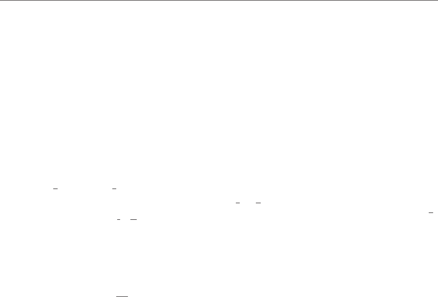
A schematic representation of the DOS for the
impurity version of the Anderson model is drawn in
Fig. 1(a). For large Coulomb repulsion U the f spec-
tral weight is split into two parts located at E
4f
(binding energy of the localized 4f electrons) and
E
4f
þU, having a width DBV
2
/W (V is the hybrid-
ization strength and W is the conduction electron
bandwidth). Due to the removal of spin degrees of
freedom, a narrow many body resonance occurs in
the vicinity of the Fermi energy E
F
as a consequence
of the crossing of the d- and f bands at the Fermi
energy (Martin 1982). IV follows immediately from
the Anderson Hamiltonian for E
4f
- E
F
. The Kondo
effect, on the contrary, is described by this model, if
E
4f
and E
4f
þU are well separated from the Fermi
level (see Kondo Systems and Heavy Fermions: Trans-
port Phenomena).
In the case of a periodic arrangement of the mag-
netic ions, a two peak structure with a gap devel-
ops as a result of the f-d hybridization (Fig. 1(b)).
This hybridization gap is complete if V is
~
k-inde-
pendent. However, if V vanishes at certain points
at the Brillouin zone, the gapping may become in-
complete.
If the f and d electron count is even, and if there
are no other electrons in the conduction band, the
application of Luttinger’s theorem causes E
F
to be
I
317
centered in this gap and the material will be an IV
isolator for T - 0. In fact, many examples of IV
semiconductors are known, possessing an even elec-
tron count such as YbB
12
with 52 valence electrons
per formula unit and an energy gap E
g
B5.2 meV
(Moser et al. 1985). Temperatures of the order of
100 k are then sufficient to smear out the gap and
thermally activate a huge number of carriers. Such
thermal excitations destroy the intersite quantum
coherence, responsible for the hybridization gap.
For an odd electron count, the Fermi energy
should be situated in one of the density peaks above
or below the gap, hence the material will demean as
an IV and heavy fermion metal for T - 0.
2. Experimental Evidence of Intermediate Valence
In general, the lattice parameters of an isotypic series
of rare-earth intermetallics smoothly decrease from
lanthanum to lutetium. This is attributed to the lan-
thanide contraction and ascribed to the fact that
though the electron count of the 4f shell increases, it
cannot completely screen the increase in the nuclear
charge and, therefore, the outer electrons become
constricted. However, compounds with cerium,
samarium, europium, thulium, or ytterbium may
significantly deviate from this simple dependence
since their valency can be larger or smaller than three,
thus cause a decrease or an increase of the unit cell
volume, respectively.
2.1 Samarium and Thulium Monochalcogenides
The monochalcogenides SmS, SmSe, and SmTe crys-
tallize in the f.c.c. structure and are characterized by
a semiconducting behavior owing to an energy gap E
g
between the 4f
6
and the 5d state of about 0.15, 0.45,
and 0.65 eV, respectively (Wachter 1994). CF inter-
action of cubic symmetry splits the 5d orbital into the
lower lying t
2g
band and the e
g
band.
The magnetic susceptibility of this series behaves
like an inhomogeneous mixing of Sm
2 þ
and Sm
3 þ
,
but the finite values for T - 0 imply that the ground
state is homogeneous. The valence fluctuations
render the mixture homogeneous; hence the f
5
spin
memory is lost when the configuration fluctuates
(Lawrence et al. 1981).
Pressure applied to such narrow bandgap systems
can give rise to a semiconductor-metal instability. In
fact, a first order transition was deduced for SmS at
p
c
¼6.5 kbar (Jayaraman et al. 1970), accompanied
by a volume change of about 20%. Slightly above p
c
,
SmS turns golden as the plasma edge moves into vis-
ible and IV occurs. For SmSe and SmTe the pressure-
induced valence transition is continuous and is found
at significant higher values of pressure, i.e., 45 and
60 kbar, respectively (Bucher et al. 1971).
The approach of the ions due to applied pressure
cause the Coulomb potential to increase. Thus CF
splitting of the 5d band grows and eventually leads to
an overlap with the 4f
6
state. Accordingly, the band-
gap closes and 4f electrons empty into the d states.
Upon the enhanced number of conduction electrons,
the lattice starts to shrink, so CF splitting strengthens
further, resulting in some avalanche effect and a first
order phase transition. Since the reduced lattice pa-
rameter stiffens the lattice as a whole, the trivalent
state is not attained. Rather, the process stops at
n ¼2.75 (Kaindl et al. 1984) where the gain in elec-
tronic energy is compensated by the increase of the
lattice energy. In the case of SmSe and SmTe, the gap
in the density of states at E
F
closes before the lattice
softens, and consequently only a second-order phase
transition is observed.
In the case of Tm, both EC, i.e., Tm
2 þ
(J ¼7/2)
and Tm
3 þ
(J ¼6) result in a magnetic ground state.
Such systems can exhibit long-range magnetic order
even in the IV state, which is in contrast to those
based on cerium, samarium, europium, or ytterbium.
The thulium monochalcogenides are of particular
interest. Binary compounds range from metallic
Figure 1
Schematic spectrum of the density of states of (a) the
impurity Kondo case and (b) the Kondo lattice. The
scale T
K
is expanded for clarity.
318
Intermediate Valence Systems
trivalent TmS over IV TmSe to semiconducting
divalent TmTe.
A sketch of the electronic structure and the density
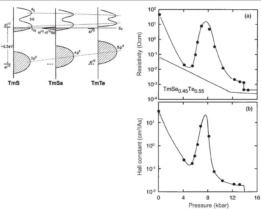
of states of this series is shown in Fig. 2 (Wachter
1994).There is a cross-over from metallic (TmSe) to
isolating behavior (TmTe). The latter exhibits the di-
valent 4f
13
EC, where the localized 4f state is sepa-
rated by an energy gap E
g
B0.3 eV from the bottom
of the 5d-t
2g
band.
When proceeding from TmTe to TmSe or TmS, the
lattice constant shrinks, thus producing chemical
pressure onto the Tm cation. Therefore, crystal field
splitting of the 5d band increases. The bottom of the
conduction band (mostly 5d-t
2g
states) may then
overlap with the 4f
13
level and 4f electrons will spill
into the conduction band.
Stoichiometric TmSe orders antiferromagnetically
below T
N
¼2.9 K (Bjerrum-Moller et al. 1977). The
electrical resistivity in both the paramagnetically and
the magnetically ordered state shows thermally acti-
vated behavior. According to Luttinger’s theorem,
TmSe should be a metal since the compound is
an odd electron system in both EC, 4f
13
and 4f
12
5d.
Antiferromagnetic order below 2.9 k, however, en-
larges the magnetic unit cell which contains an even
number (26) of electrons. The hybridization gap can
then exist with E
F
just in the center, and the system
should behave isolating. However, at m
0
H ¼0.5 T,
TmSe becomes ferromagnetic, thus the folding of the
Brillouin zone vanishes. Consequently, TmSe be-
haves metallic and the system is an IV ferromagnet
(Batlogg et al. 1977).
As for many other IV compounds with the Fermi
level within the hybridization gap, pressure applied to
TmSe (p
c
B30 kbar) will close the bandgap primarily
due to the growing overlap of the crystal field split
5d band with the 4f
13
state (Wachter 1994).
Besides, the pseudobinary TmSe
1x
Te
x
allows to
realize a novel feature in condensed matter physics,
the excitonic insulator, which is characterized by a
Bose-Einstein condensation of quasi-particles into a
coherent exciton phase (Neuenschwander and Wach-
ter 1990). Figure 3 shows the pressure dependence of
the electrical resistivity of TmSe
0.45
Te
0.55
at high and
low temperatures and the Hall constant. The most
striking feature with respect to the resistivity at
T ¼4 K is that after the expected initial decrease of
r(p), a rapid rise in a narrow pressure range from
about 5 kbar to 8 kbar occurs. Beyond this pressure,
the resistivity decreases again and furthermore ex-
hibits a first order phase transition near p ¼14 kbar.
Figure 2
Electronic structure and density of states of the Tm
monochalcogenides normalized to the Fermi energy E
F
(dotted line). The dashed lines through the density of
state peaks serve as a guide to the eyes.
Figure 3
(a) Pressure dependence of the resistivity of
TmSe
0.45
Te
0.55
at 300 K (lower curve) and at 4.2 K
(upper curve). At 300 K the semiconducting to metal
transition is at p
c
¼11.5 kbar and for T ¼4.2 K at
p
c
B14 kbar. (b) Pressure-dependent Hall constant R
H
at 4.2 K.
319
Intermediate Valence Systems