Bird J. Electrical Circuit Theory and Technology
Подождите немного. Документ загружается.


12 Transistors
At the end of this chapter you should be able to:
ž understand the structure of a bipolar junction transistor
ž understand transistor action for p-n-p and n-p-n types
ž draw the circuit diagram symbols for p-n-p and n-p-n
transistors
ž appreciate common-base, common-emitter and
common-collector transistor connections
ž interpret transistor characteristics
ž appreciate how the transistor is used as an amplifier
ž determine the load line on transistor characteristics
ž estimate current, voltage and power gains from transistor
characteristics
ž understand thermal runaway in a transistor
12.1 The bipolar
junction transistor
The bipolar junction transistor consists of three regions of semiconductor
material. One type is called a p-n-p transistor, in which two regions of
p-type material sandwich a very thin layer of n-type material. A second
type is called an n-p-n transistor, in which two regions of n-type material
sandwich a very thin layer of p-type material. Both of these types of tran-
sistors consist of two p-n junctions placed very close to one another in
a back-to-back arrangement on a single piece of semiconductor mate-
rial. Diagrams depicting these two types of transistors are shown in
Figure 12.1.
The two p-type material regions of the p-n-p transistor are called the
emitter and collector and the n-type material is called the base. Similarly,
the two n-type material regions of the n-p-n transistor are called the
emitter and collector and the p-type material region is called the base, as
shown in Figure 12.1.
Transistors have three connecting leads and in operation an electrical
input to one pair of connections, say the emitter and base connections
can control the output from another pair, say the collector and emitter
connections. This type of operation is achieved by appropriately biasing
the two internal p-n junctions. When batteries and resistors are connected
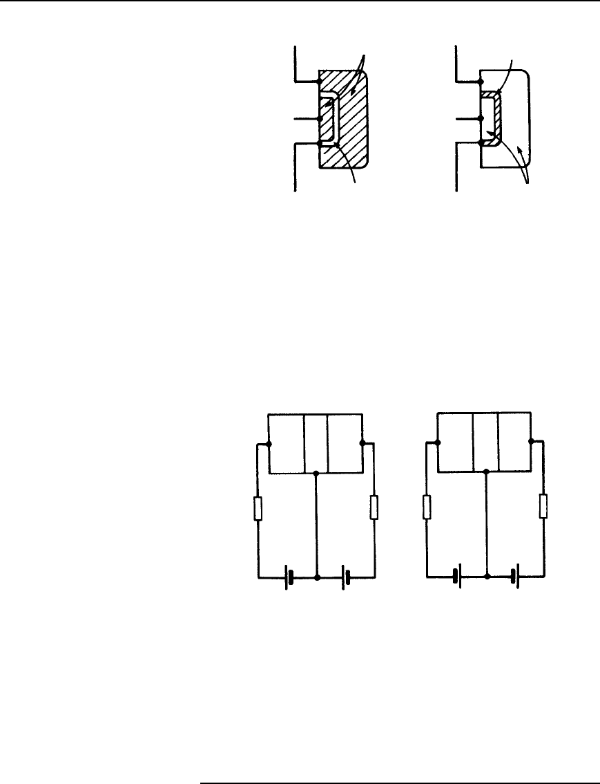
to a p-n-p transistor, as shown in Figure 12.2(a), the base-emitter junction
is forward biased and the base-collector junction is reverse biased.
Similarly, an n-p-n transistor has its base-emitter junction forward
biased and its base-collector junction reverse biased when the batteries
are connected as shown in Figure 12.2(b).
146 Electrical Circuit Theory and Technology
Collector
Emitter
Base
Collector
Emitter
Base
n-type
material
n-type
material
p-type
material
p-type
material
p-n-p transistor n-p-n transistor
Figure 12.1
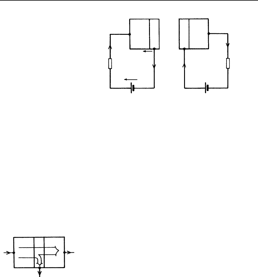
For a silicon p-n-p transistor, biased as shown in Figure 12.2(a), if the
base-emitter junction is considered on its own, it is forward biased and
a current flows. This is depicted in Figure 12.3(a). For example, if R
E
is 1000 , the battery is 4.5V and the voltage drop across the junction
is taken as 0.7V, the current flowing is given by 4.5 0.7/1000 D
3.8mA.
Emitter Base Collector Emitter Base Collector
Emitter
resistor
Load
resistor
Emitter
resistor
Load
resistor
+
+
−− +
−+− −+−+
pnp npn
(a) p-n-p transistor (b) n-p-n transistor
Figure 12.2
When the base-collector junction is considered on its own, as shown in
Figure 12.3(b), it is reverse biased and the collector current is something
less than 1
µA.
However, when both external circuits are connected to the transistor,
most of the 3.8mA of current flowing in the emitter, which previously
flowed from the base connection, now flows out through the collector
connection due to transistor action.
Transistors 147
+− +−
4.5 V
R
E
= 1000 Ω
I
E
I
C
R
L
0.7 V
Emitter Base
ppnn
Base Collector
(a) (b)
Figure 12.3
12.2 Transistor action
In a p-n-p transistor, connected as shown in Figure 12.2(a), transistor
action is accounted for as follows:
(a) The majority carriers in the emitter p-type material are holes
(b) The base-emitter junction is forward biased to the majority carriers
and the holes cross the junction and appear in the base region
(c) The base region is very thin and is only lightly doped with electrons
so although some electron-hole pairs are formed, many holes are left
in the base region
(d) The base-collector junction is reverse biased to electrons in the base
region and holes in the collector region, but forward biased to holes
in the base region; these holes are attracted by the negative potential
at the collector terminal
(e) A large proportion of the holes in the base region cross the base-
collector junction into the collector region, creating a collector cur-
rent; conventional current flow is in the direction of hole movement.
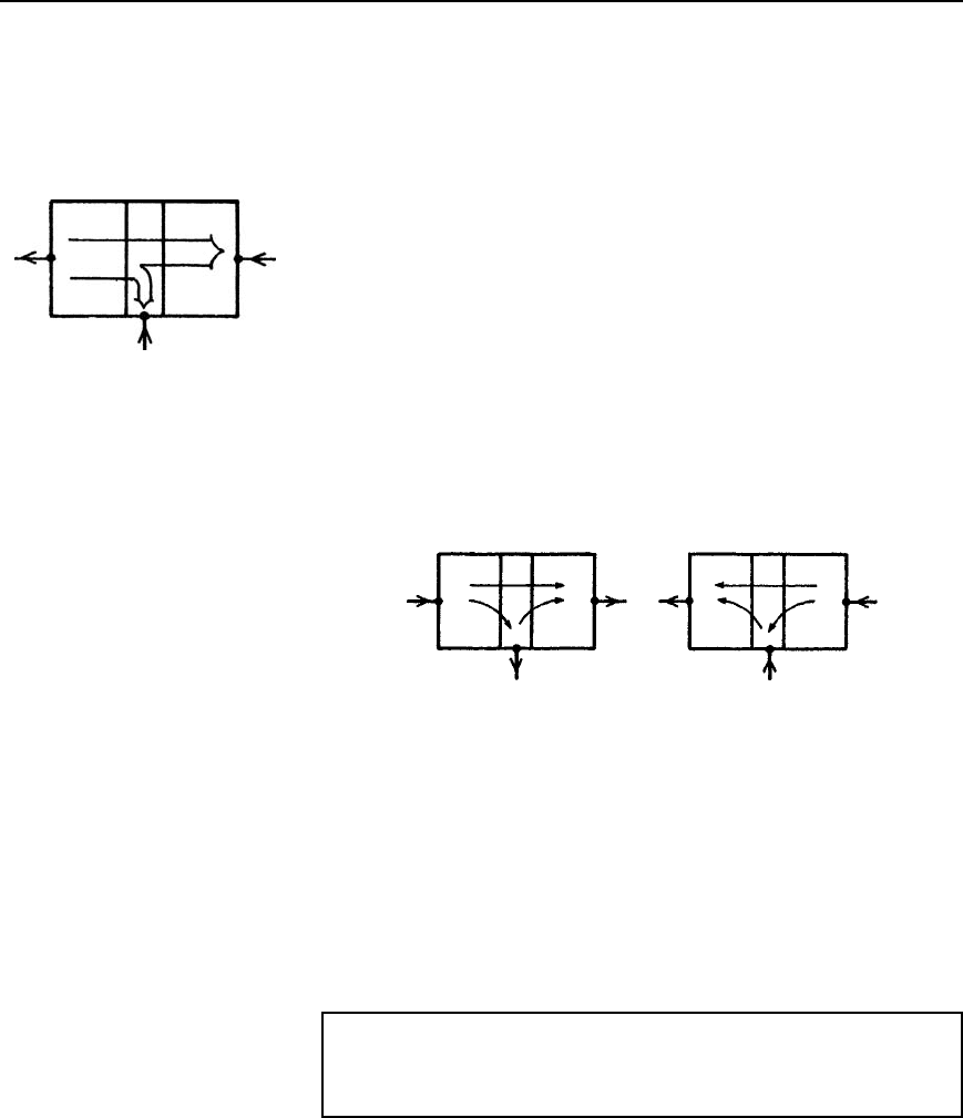
The transistor action is shown diagrammatically in Figure 12.4. For tran-
sistors having very thin base regions, up to 99.5% of the holes leaving
the emitter cross the base collector junction.
In an n-p-n transistor, connected as shown in Figure 12.2(b), transistor
action is accounted for as follows:
(a) The majority carriers in the n-type emitter material are electrons
Emitter Base Collector
Holes
p
I
E
I
C
I
B
np
Figure 12.4
(b) The base-emitter junction is forward biased to these majority carriers
and electrons cross the junction and appear in the base region
(c) The base region is very thin and only lightly doped with holes, so
some recombination with holes occurs but many electrons are left
in the base region
(d) The base-collector junction is reverse biased to holes in the base
region and electrons in the collector region, but is forward biased
148 Electrical Circuit Theory and Technology
to electrons in the base region; these electrons are attracted by the
positive potential at the collector terminal
(e) A large proportion of the electrons in the base region cross the
base collector junction into the collector region, creating a collector
current.
The transistor action is shown diagrammatically in Figure 12.5. As stated
in Section 12.1, conventional current flow is taken to be in the direction
of hole flow, that is, in the opposite direction to electron flow, hence the
directions of the conventional current flow are as shown in Figure 12.5.
For a p-n-p transistor, the base-collector junction is reverse biased for
majority carriers. However, a small leakage current, I
CBO
flows from
the base to the collector due to thermally generated minority carriers
(electrons in the collector and holes in the base), being present.
Emitter Base Collector
Electrons
n
I
E
I
C
I
B
pn
+−
Figure 12.5
The base-collector junction is forward biased to these minority carriers.
If a proportion, ˛, (having a value of up to 0.995 in modern transistors),
of the holes passing into the base from the emitter, pass through the base-
collector junction, then the various currents flowing in a p-n-p transistor
are as shown in Figure 12.6(a).
Emitter Base Collector Emitter Base Collector
pn n npp
I
E
I
E
I
C
I
C
I
CBO
I
CBO
I
B
I
B
∝
I
E
∝
I
E
(1−∝)
I
E
(1−∝)
I
E
(a) (b)
Figure 12.6
Similarly, for an n-p-n transistor, the base-collector junction is reversed
biased for majority carriers, but a small leakage current, I
CBO
flows from
the collector to the base due to thermally generated minority carriers
(holes in the collector and electrons in the base), being present. The
base-collector junction is forward biased to these minority carriers. If a
proportion, ˛, of the electrons passing through the base-emitter junction
also pass through the base-collector junction then the currents flowing in
an n-p-n transistor are as shown in Figure 12.6(b).
Problem 1. With reference to a p-n-p transistor, explain briefly
what is meant by the term transistor action and why a bipolar
junction transistor is so named.
For the transistor as depicted in Figure 12.4, the emitter is relatively
heavily doped with acceptor atoms (holes). When the emitter terminal
is made sufficiently positive with respect to the base, the base-emitter
junction is forward biased to the majority carriers. The majority carriers
are holes in the emitter and these drift from the emitter to the base. The
Transistors 149
base region is relatively lightly doped with donor atoms (electrons) and
although some electron-hole recombination’s take place, perhaps 0.5%,
most of the holes entering the base, do not combine with electrons.
The base-collector junction is reverse biased to electrons in the base
region, but forward biased to holes in the base region. Since the base is
very thin and now is packed with holes, these holes pass the base-emitter
junction towards the negative potential of the collector terminal. The
control of current from emitter to collector is largely independent of the
collector-base voltage and almost wholly governed by the emitter-base
voltage. The essence of transistor action is this current control by means
of the base-emitter voltage.
In a p-n-p transistor, holes in the emitter and collector regions are
majority carriers, but are minority carriers when in the base region. Also
thermally generated electrons in the emitter and collector regions are
minority carriers as are holes the base region. However, both majority
and minority carriers contribute towards the total current flow (see
Figure 12.6(a)). It is because a transistor makes use of both types of
charge carriers (holes and electrons) that they are called bipolar. The
transistor also comprises two p-n junctions and for this reason it is a
junction transistor. Hence the name —bipolar junction transistor.
(0 V)
(0 V)
e
e
b
b
c
c
(−6 V)
(6 V)
(−0.6 V)
(0.6 V)
p-n-p transistor
n-p-n transistor
Figure 12.7
12.3 Transistor symbols
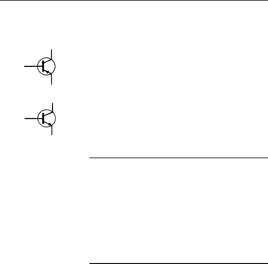
Symbols are used to represent p-n-p and n-p-n transistors in circuit dia-
grams and are as shown in Figure 12.7. The arrowhead drawn on the
emitter of the symbol is in the direction of conventional emitter current
(hole flow). The potentials marked at the collector, base and emitter are
typical values for a silicon transistor having a potential difference of 6V
between its collector and its emitter.
The voltage of 0.6 V across the base and emitter is that required to
reduce the potential barrier and if it is raised slightly to, say, 0.62 V, it is
likely that the collector current will double to about 2 mA. Thus a small
change of voltage between the emitter and the base can give a relatively
large change of current in the emitter circuit; because of this, transistors
can be used as amplifiers.
12.4 Transistor
connections
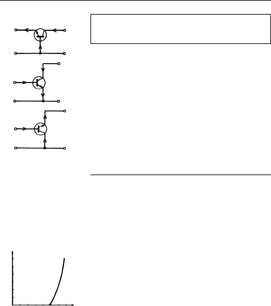
There are three ways of connecting a transistor, depending on the use
to which it is being put. The ways are classified by the electrode that is
common to both the input and the output. They are called:
(a) common-base configuration, shown in Figure 12.8(a)
(b) common-emitter configuration, shown in Figure 12.8(b)
(c) common-collector configuration, shown in Figure 12.8(c)
These configurations are for an n-p-n transistor. The current flows shown
are all reversed for a p-n-p transistor.
150 Electrical Circuit Theory and Technology
Problem 2. The basic construction of an n-p-n transistor makes it
appear that the emitter and collector can be interchanged. Explain
why this is not usually done.
In principle, a bipolar junction transistor will work equally well with either
the emitter or collector acting as the emitter. However, the conventional
emitter current largely flows from the collector through the base to the
emitter, hence the emitter region is far more heavily doped with donor
atoms (electrons) than the base is with acceptor atoms (holes). Also, the
base-collector junction is normally reverse biased and in general, doping
density increases the electric field in the junction and so lowers the break-
down voltage. Thus, to achieve a high breakdown voltage, the collector
region is relatively lightly doped.
In addition, in most transistors, the method of production is to diffuse
acceptor and donor atoms onto the n-type semiconductor material, one
after the other, so that one overrides the other. When this is done, the
doping density in the base region is not uniform but decreases from emitter
to collector. This results in increasing the effectiveness of the transistor.
Thus, because of the doping densities in the three regions and the non-
uniform density in the base, the collector and emitter terminals of a tran-
sistor should not be interchanged when making transistor connections.
I
E
I
B
I
B
I
C
I
E
I
E
I
C
I
B
I
C
e
INPUT
INPUT
INPUT
OUTPUT
OUTPUT
OUTPUT
c
b
(a)
(b)
(c)
Figure 12.8
12.5 Transistor
characteristics
The effect of changing one or more of the various voltages and currents
associated with a transistor circuit can be shown graphically and these
graphs are called the characteristics of the transistor. As there are five
variables (collector, base and emitter currents and voltages across the
collector and base and emitter and base) and also three configurations,
many characteristics are possible. Some of the possible characteristics are
given below.
(a) Common-base configuration
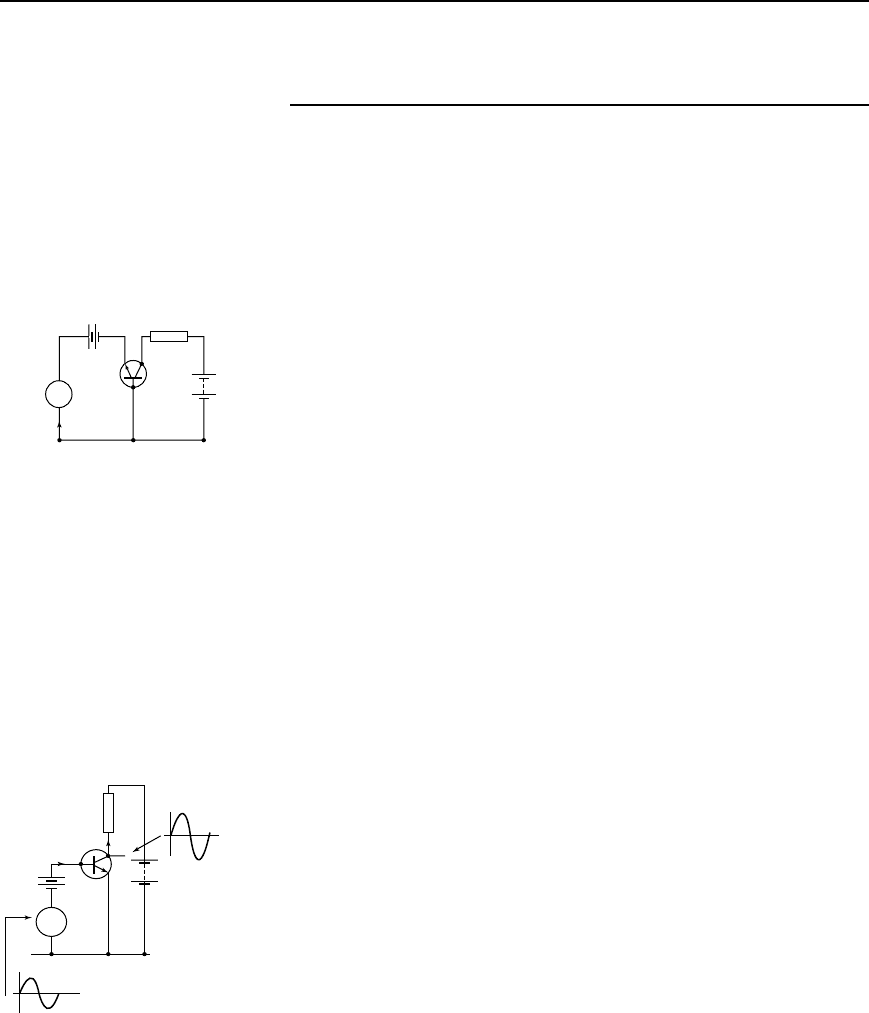
(i) Input characteristic. With reference to Figure 12.8(a), the input to
a common-base transistor is the emitter current, I
E
, and can be varied
by altering the base emitter voltage V
EB
. The base-emitter junction is
essentially a forward biased junction diode, so as V
EB
is varied, the current
flowing is similar to that for a junction diode, as shown in Figure 12.9
for a silicon transistor. Figure 12.9 is called the input characteristic for
an n-p-n transistor having common-base configuration. The variation of
the collector-base voltage V
CB
has little effect on the characteristic. A
similar characteristic can be obtained for a p-n-p transistor, these having
reversed polarities.
0
0.2 0.4 0.6 −
V
EB
Emitter base voltage (V)
1
2
3
4
5
6
−
I
E
Emitter current (mA)
Figure 12.9
(ii) Output characteristics. The value of the collector current I
C
is very
largely determined by the emitter current, I
E
. For a given value of I
E
the collector-base voltage, V
CB
, can be varied and has little effect on the
value of I
C
.IfV
CB
is made slightly negative, the collector no longer

Transistors 151
attracts the majority carriers leaving the emitter and I
C
falls rapidly to
zero. A family of curves for various values of I
E
are possible and some
of these are shown in Figure 12.10. Figure 12.10 is called the output
characteristics for an n-p-n transistor having common-base configuration.
Similar characteristics can be obtained for a p-n-p transistor, these having
reversed polarities.
−20 2 4 6 8
V
CB
I
E
= 30 mA
I
E
= 20 mA
I
E
= 10 mA
I
C
Collector current (mA)
30
20
10
Collector-base voltage (V)
Figure 12.10
(b) Common-emitter configuration
(i) Input characteristic. In a common-emitter configuration (see
Figure 12.8(b)), the base current is now the input current. As V
EB
is
varied, the characteristic obtained is similar in shape to the input char-
acteristic for a common-base configuration shown in Figure 12.9, but the
values of current are far less. With reference to Figure 12.6(a), as long
as the junctions are biased as described, the three currents I
E
, I
C
and I
B
keep the ratio 1 : ˛ : 1 ˛, whichever configuration is adopted. Thus
the base current changes are much smaller than the corresponding emitter
current changes and the input characteristic for an n-p-n transistor is as
shown in Figure 12.11. A similar characteristic can be obtained for a
p-n-p transistor, these having reversed polarities.
(ii) Output characteristics. A family of curves can be obtained, depen-
ding on the value of base current I
B
and some of these for an n-p-n
transistor are shown in Figure 12.12. A similar set of characteristics can
be obtained for a p-n-p transistor, these having reversed polarities. These
characteristics differ from the common base output characteristics in two
ways:
the collector current reduces to zero without having to reverse the
collector voltage, and
0 0.2 0.4 0.6 0.8
V
BE
Base-emitter voltage (V)
50
100
150
200
250
300
Base current (µA)
I
B
Figure 12.11
the characteristics slope upwards indicating a lower output resistance
(usually kilohms for a common-emitter configuration compared with
megohms for a common-base configuration).
Problem 3. With the aid of a circuit diagram, explain how the
input and output characteristics of an n-p-n transistor having a
common-base configuration can be obtained.
A circuit diagram for obtaining the input and output characteristics
for an n-p-n transistor connected in common-base configuration is shown
in Figure 12.13. The input characteristic can be obtained by varying R
1
,
which varies V
EB
, and noting the corresponding values of I
E
. This is
repeated for various values of V
CB
. It will be found that the input char-
acteristic is almost independent of V
CB
and it is usual to give only one
characteristic, as shown in Figure 12.9.
10
0246810
20
30
40
50
V
CE
Collector-emitter voltage (V)
Collector current (mA)
I
C
I
B
= 300 µA
I
B
= 250 µA
I
B
= 200 µA
I
B
= 150 µA
I
B
= 100 µA
I
B
= 50 µA
I
B
= 0
Figure 12.12
To obtain the output characteristics, as shown in Figure 12.10, I
E
is
set to a suitable value by adjusting R
1
. For various values of V
CB
,setby
adjusting R
2
, I
C
is noted. This procedure is repeated for various values of
I
E
. To obtain the full characteristics, the polarity of battery V
2
hastobe
reversed to reduce I
C
to zero. This must be done very carefully or else
I
E
I
C
I
B
V
CB
V
EB
V
2
R
2
R
1
A
A
−
+
−
+
A
V
V
Figure 12.13
152 Electrical Circuit Theory and Technology
values of I
C
will rapidly increase in the reverse direction and burn out
the transistor.
12.6 The transistor as an
amplifier
The amplifying properties of a transistor depend upon the fact that current
flowing in a low-resistance circuit is transferred to a high-resistance circuit
with negligible change in magnitude. If the current then flows through a
load resistance, a voltage is developed. This voltage can be many times
greater than the input voltage which caused the original current flow.
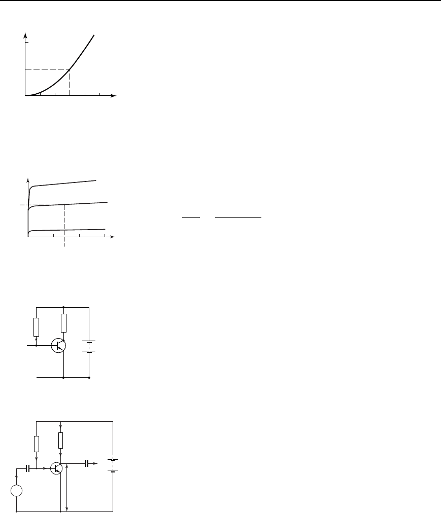
(a) Common-base amplifier
The basic circuit for a transistor is shown in Figure 12.14 where an n-
p-n transistor is biased with batteries b
1
and b
2
. A sinusoidal alternating
input signal,
v
e
, is placed in series with the input bias voltage, and a load
resistor, R
L
, is placed in series with the collector bias voltage. The input
signal is therefore the sinusoidal current i
e
resulting from the applica-
tion of the sinusoidal voltage
v
e
superimposed on the direct current I
E
established by the base-emitter voltage V
BE
.
~
v
e
R
L
I
E
+
i
e
b
1
b
2
Figure 12.14
Let the signal voltage
v
e
be 100mV and the base-emitter circuit resis-
tance be 50. Then the emitter signal current will be 100/50 D 2mA.
Let the load resistance R
L
D 2.5k. About 0.99 of the emitter current will
flow in R
L
. Hence the collector signal current will be about 0.99 ð2 D
1.98mA and the signal voltage across the load will be 2500 ð 1.98 ð
10
3
D 4.95V. Thus a signal voltage of 100 mV at the emitter has produ-
ced a voltage of 4950 mV across the load. The voltage amplification or
gain is therefore 4950/100 D 49.5 times. This example illustrates the
action of a common-base amplifier where the input signal is applied
between emitter and base and the output is taken from between collector
and base.
~
R
L
7V
V
CC
V
BB
5mA
12 V
1kΩ
I
B
+
i
b
i
b
+
−
−
+
0.1 mA
base d.c.
bias
I
B
Collector
voltage
variations
Figure 12.15
(b) Common-emitter amplifier
The basic circuit arrangement of a common-emitter amplifier is shown
in Figure 12.15. Although two batteries are shown, it is more usual to
employ only one to supply all the necessary bias. The input signal is
applied between base and emitter, and the load resistor R
L
is connected
between collector and emitter. Let the base bias battery provide a voltage
which causes a base current I
B
of 0.1mA to flow. This value of base
current determines the mean d.c. level upon which the a.c. input signal
will be superimposed. This is the d.c. base current operating point.
Let the static current gain of the transistor, ˛
E
, be 50. Since 0.1mA
is the steady base current, the collector current I
C
will be ˛
E
ð I
B
D
50 ð 0.1 D 5 mA. This current will flow through the load resistor R
L
(D 1k), and there will be a steady voltage drop across R
L
given by
I
C
R
L
D 5 ð 10
3
ð 1000 D 5V. The voltage at the collector, V
CE
, will
therefore be V
CC
I
C
R
L
D 12 5 D 7 V. This value of V
CE
is the mean
(or quiescent) level about which the output signal voltage will swing alter-
nately positive and negative. This is the collector voltage d.c. operating
Transistors 153
I
B
(µA)
200
100
0 0.5 1.0
V
BE
(V)
X
Figure 12.16
point. Both of these d.c. operating points can be pin-pointed on the
input and output characteristics of the transistor. Figure 12.16 shows
the I
B
/V
BE
characteristic with the operating point X positioned at I
B
D
100
µA, V
BE
D 0.75V, say.
Figure 12.17 shows the I
C
/V
CE
characteristics, with the operating point
Y positioned at I
C
D 5mA,V
CE
D 7V. It is usual to choose the operating
point Y somewhere near the centre of the graph.
I
C
(mA)
V
CE
(V)
I
B
= 100µA
5 mA
mean
collector
current
0
51015
7 V mean collector
voltage
Y
Figure 12.17
It is possible to remove the bias battery V
BB
and obtain base bias from
the collector supply battery V
CC
instead. The simplest way to do this is
to connect a bias resistor R
B
between the positive terminal of the V
CC
supply and the base as shown in Figure 12.18. The resistor must be of
such a value that it allows 100
µA to flow in the base-emitter diode.
V
CC
R
L
R
B
l
B
Figure 12.18
For a silicon transistor, the voltage drop across the junction for forward
bias conditions is about 0.6 V. The voltage across R
B
must then be 12
0.6 D 11.4V. Hence, the value of R
B
must be such that I
B
ð R
B
D 11.4V,
i.e.
R
B
D
11.4
I
B
D
11.4
100 ð 10
6
D 114k.
With the inclusion of the 1k load resistor, R
L
, a steady 5mA collector
current, and a collector-emitter voltage of 7 V, the d.c. conditions are
established.
An alternating input signal (
v
i
) can now be applied. In order not to
disturb the bias condition established at the base, the input must be fed to
the base by way of a capacitor C
1
. This will permit the alternating signal
to pass to the base but will prevent the passage of direct current. The
reactance of this capacitor must be such that it is very small compared
with the input resistance of the transistor. The circuit of the amplifier is
now as shown in Figure 12.19. The a.c. conditions can now be determined.
~
−
+
v
0
C
1
v
i
C
2
V
CE
V
CC
i
b
l
B
l
B
+
i
b
R
B
R
L
i
c
= α
e
i
b
l
C
+
i
c
Figure 12.19
When an alternating signal voltage
v
1
is applied to the base via capacitor
C
1
the base current i
b
varies. When the input signal swings positive, the
base current increases; when the signal swings negative, the base current
decreases. The base current consists of two components: I
B
, the static base
bias established by R
B
,andi
b
, the signal current. The current variation
i
b
will in turn vary the collector current, i
c
. The relationship between i
c
and i
b
is given by i
c
D ˛
e
i
b
, where ˛
e
is the dynamic current gain of
the transistor and is not quite the same as the static current gain ˛
E
; the
difference is usually small enough to be insignificant.
The current through the load resistor R
L
also consists of two compo-
nents: I
C
, the static collector current, and i
c
, the signal current. As i
b
increases, so does i
c
and so does the voltage drop across R
L
. Hence, from
the circuit:
V
CE
D V
CC
I
C
C i
c
R
L
The d.c. components of this equation, though necessary for the amplifier
to operate at all, need not be considered when the a.c. signal conditions
are being examined. Hence, the signal voltage variation relationship is:
v
ce
D˛
e
ð i
b
ð R
L
D i
c
R
L
154 Electrical Circuit Theory and Technology
the negative sign being added because v
ce
decreases when i
b
increases and
vice versa. The signal output and input voltages are of opposite polarity,
i.e. a phase shift of 180
°
has occurred. So that the collector d.c. potential
is not passed on to the following stage, a second capacitor, C
2
, is added
as shown in Figure 12.19. This removes the direct component but permits
the signal voltage
v
o
D i
c
R
L
to pass to the output terminals.
12.7 The load line
The relationship between the collector-emitter voltage (V
CE
) and collector
current (I
C
) is given by the equation: V
CE
D V
CC
I
C
R
L
in terms of the
d.c. conditions. Since V
CC
and R
L
are constant in any given circuit, this
represents the equation of a straight line which can be written in the
y D mx Cc form. Transposing V
CE
D V
CC
I
C
R
L
for I
C
gives:
I
C
D
V
CC
V
CE
R
L
D
V
CC
R
L
V
CE
R
L
D
1
R
L
V
CE
C
V
CC
R
L
i.e. I
C
D
1
R
L
V
CE
C
V
CC
R
L
which is of the straight line form y D mx C c; hence if I
c
is plotted
vertically and V
CE
horizontally, then the gradient is given by 1/R
L
and the vertical axis intercept is V
CC
/R
L
.
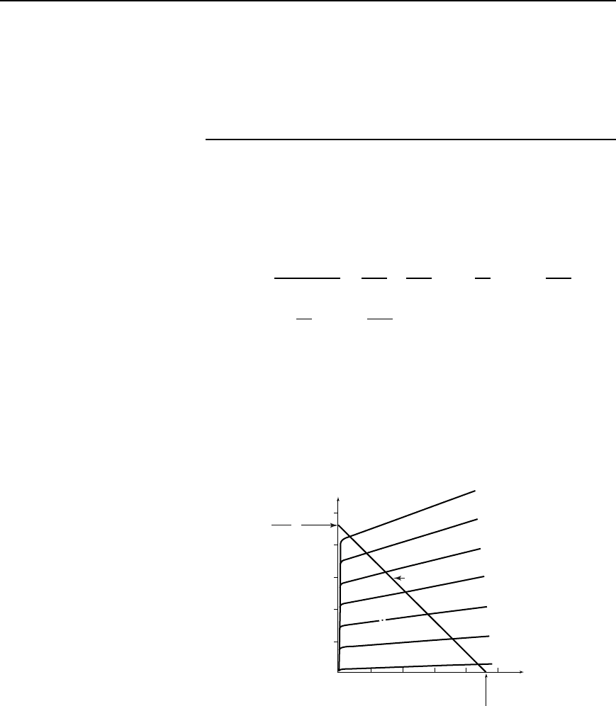
A family of collector static characteristics drawn on such axes is shown
in Figure 12.12 on page 151, and so the line may be superimposed on
these as shown in Figure 12.20.
20
10
20
30
40
50
46810
V
CE
V
CC
Collector-emitter voltage (V)
Collector current (mA)
I
C
V
CC
R
L
A
B
I
B
= 0
I
B
= 50 µA
I
B
= 100 µA
I
B
= 200 µA
I
B
= 250 µA
I
B
= 300 µA
LOAD LINE
V
CE
=
V
CC
−
I
C
R
L
Figure 12.20
The reason why this line is necessary is because the static curves relate
I
C
to V
CE
for a series of fixed values of I
B
. When a signal is applied to
