Bird J. Electrical Circuit Theory and Technology
Подождите немного. Документ загружается.


Electrical measuring instruments and measurements 135
Determine the decibel power ratio for each.
[(a) 10 dB (b) 4.77 dB (c) 16.02 dB (d) 20 dB]
13 The input and output currents of a system are 2 mA and 10 mA
respectively. Determine the decibel current ratio of output to input
current assuming input and output resistances of the system are equal.
[13.98 dB]
14 5% of the power supplied to a cable appears at the output terminals.
Determine the power loss in decibels. [13 dB]
15 An amplifier has a gain of 24 dB. Its input power is 10 mW. Find
its output power. [2.51 W]
16 The output voltage from an amplifier is 7 mV. If the voltage gain
is 25 dB calculate the value of the input voltage assuming that the
amplifier input resistance and load resistance are equal. [0.39 mV]
17 The scale of a voltmeter has a decibel scale added to it, which is
calibrated by taking a reference level of 0 dB when a power of 1 mW
is dissipated in a 600 resistor. Determine the voltage at (a) 0 dB
(b) 1.5 dB and (c) 15 dB (d) What decibel reading corresponds to
0.5 V? [(a) 0.775 V (b) 0.921 V (c) 0.138 V (d) 3.807 dB]
Wheatstone bridge and d.c. potentiometer
18 In a Wheatstone bridge PQRS, a galvanometer is connected between
Q and S and a voltage source between P and R. An unknown resistor
R
x
is connected between P and Q. When the bridge is balanced, the
resistance between Q and R is 200 , that between R and S is 10
and that between S and P is 150 . Calculate the value of R
x
[3 k]
19 Balance is obtained in a d.c. potentiometer at a length of 31.2 cm
when using a standard cell of 1.0186 volts. Calculate the e.m.f. of a
dry cell if balance is obtained with a length of 46.7 cm. [1.525 V]
20 A Wheatstone bridge PQRS has the following arm resistances:
PQ, 1 k š 2%; QR, 100 š 0.5%; RS, unknown resistance; SP,
273.6 š 0.1%. Determine the value of the unknown resistance,
and its accuracy of measurement.
[27.36 š 2.6% or 27.36 š 0.71 ]
Measurement errors
21 The p.d. across a resistor is measured as 37.5 V with an accuracy
of š0.5%. The value of the resistor is 6 k š 0.8%. Determine the
current flowing in the resistor and its accuracy of measurement.
[6.25 mA š1.3% or 6.25š 0.08 mA]
22 The voltage across a resistor is measured by a 75 V f.s.d. voltmeter
which gives an indication of 52 V. The current flowing in the resistor
is measured by a 20 A f.s.d. ammeter which gives an indication of

136 Electrical Circuit Theory and Technology
12.5 A. Determine the resistance of the resistor and its accuracy if
both instruments have an accuracy of š2% of f.s.d.
[4.16 š 6.08% or 4.16 š 0.25 ]
23 A 240 V supply is connected across a load resistance R. Also
connected across R is a voltmeter having a f.s.d. of 300 V and a figure
of merit (i.e. sensitivity) of 8 k/V. Calculate the power dissipated
by the voltmeter and by the load resistance if (a) R D 100 (b) R D
1M. Comment on the results obtained.
[(a) 24 mW, 576 W (b) 24 mW, 57.6 mW]

11 Semiconductor diodes
At the end of this chapter you should be able to:
ž classify materials as conductors, semiconductors or insulators
ž appreciate the importance of silicon and germanium
ž understand n-type and p-type materials
ž understand the p-n junction
ž appreciate forward and reverse bias of p-n junctions
ž draw the circuit diagram symbol for a semiconductor diode
11.1 Types of materials
Materials may be classified as conductors, semiconductors or insulators.
The classification depends on the value of resistivity of the material. Good
conductors are usually metals and have resistivities in the order of 10
7
to 10
8
m, semiconductors have resistivities in the order of 10
3
to
3 ð 10
3
m and the resistivities of insulators are in the order of 10
4
to
10
14
m. Some typical approximate values at normal room temperatures
are:
Conductors:
Aluminium 2.7 ð 10
8
m
Brass (70 Cu/30 Zn) 8 ð 10
8
m
Copper (pure annealed) 1.7 ð 10
8
m
Steel (mild) 15 ð10
8
m
Semiconductors:
Silicon 2.3 ð 10
3
m
at 27
°
C
Germanium 0.45m
Insulators:
Glass ½ 10
10
m
Mica ½ 10
11
m
PVC ½ 10
13
m
Rubber (pure) 10
12
to 10
14
m
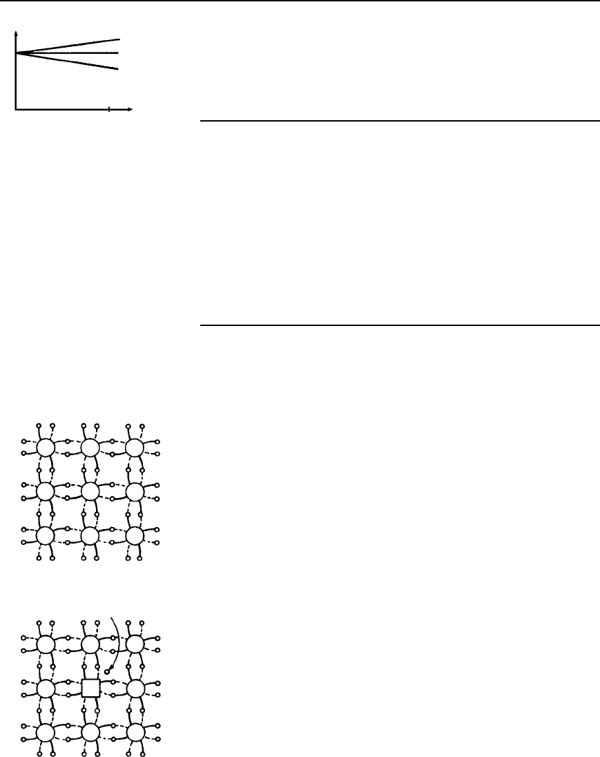
In general, over a limited range of temperatures, the resistance of a
conductor increases with temperature increase, the resistance of insula-
tors remains approximately constant with variation of temperature and

138 Electrical Circuit Theory and Technology
15
t
Temperature °C
Conductor
Insulator
Semiconductor
Resistance Ω
Figure 11.1
the resistance of semiconductor materials decreases as the temperature
increases. For a specimen of each of these materials, having the same
resistance (and thus completely different dimensions), at say, 15
°
C, the
variation for a small increase in temperature to t
°
C is as shown in
Figure 11.1.
11.2 Silicon and
germanium
The most important semiconductors used in the electronics industry are
silicon and germanium. As the temperature of these materials is raised
above room temperature, the resistivity is reduced and ultimately a point
is reached where they effectively become conductors. For this reason,
silicon should not operate at a working temperature in excess of 150
°
Cto
200
°
C, depending on its purity, and germanium should not operate at a
working temperature in excess of 75
°
Cto90
°
C, depending on its purity.
As the temperature of a semiconductor is reduced below normal room
temperature, the resistivity increases until, at very low temperatures the
semiconductor becomes an insulator.
11.3 n-type and p-type
materials
Adding extremely small amounts of impurities to pure semiconductors in a
controlled manner is called doping. Antimony, arsenic and phosphorus are
called n-type impurities and form an n-type material when any of these
impurities are added to silicon or germanium. The amount of impurity
added usually varies from 1 part impurity in 10
5
parts semiconductor
material to 1 part impurity to 10
8
parts semiconductor material, depending
on the resistivity required. Indium, aluminium and boron are called p-type
impurities and form a p-type material when any of these impurities are
added to a semiconductor.
In semiconductor materials, there are very few charge carriers per unit
volume free to conduct. This is because the ‘four electron structure’ in
the outer shell of the atoms (called valency electrons), form strong cova-
lent bonds with neighbouring atoms, resulting in a tetrahedral structure
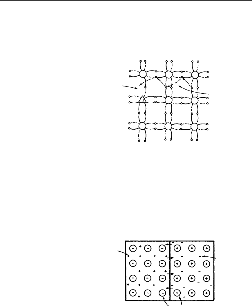
with the electrons held fairly rigidly in place. A two-dimensional diagram
depicting this is shown for germanium in Figure 11.2.
Ge Ge Ge
Ge Ge
Ge
Ge
Ge
Ge
Figure 11.2
Arsenic, antimony and phosphorus have five valency electrons and
when a semiconductor is doped with one of these substances, some impu-
rity atoms are incorporated in the tetrahedral structure. The ‘fifth’ valency
electron is not rigidly bonded and is free to conduct, the impurity atom
donating a charge carrier. A two-dimensional diagram depicting this is
shown in Figure 11.3, in which a phosphorus atom has replaced one of
the germanium atoms. The resulting material is called n-type material,
and contains free electrons.
Indium, aluminium and boron have three valency electrons and when a
semiconductor is doped with one of these substances, some of the semi-
conductor atoms are replaced by impurity atoms. One of the four bonds
associated with the semiconductor material is deficient by one electron
and this deficiency is called a hole. Holes give rise to conduction when
Ge Ge Ge
GePGe
Ge
Ge
Ge
Free electron
Figure 11.3

Semiconductor diodes 139
a potential difference exists across the semiconductor material due to
movement of electrons from one hole to another, as shown in Figure 11.4.
In this figure, an electron moves from A to B, giving the appearance that
the hole moves from B to A. Then electron C moves to A, giving the
appearance that the hole moves to C, and so on. The resulting material is
p-type material containing holes.
Ge
Ge
Ge
Ge
Ge
Ge
Ge
Ge
A
Hole
(missing
electron)
B
C
A
1
2
3
4
Possible
movements
of electrons
Figure 11.4
11.4 The p-n junction
A p-n junction is piece of semiconductor material in which part of the
material is p-type and part is n-type. In order to examine the charge
situation, assume that separate blocks of p-type and n-type materials are
pushed together. Also assume that a hole is a positive charge carrier and
that an electron is a negative charge carrier.
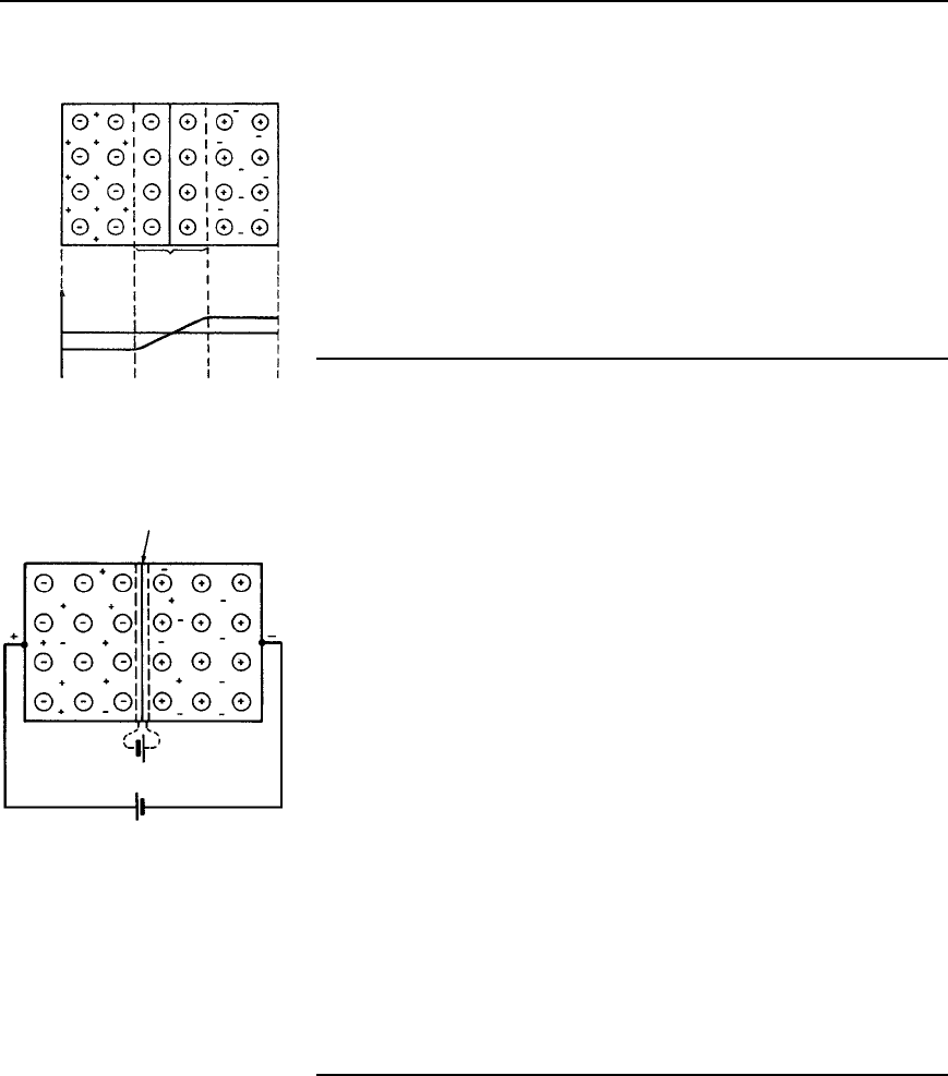
At the junction, the donated electrons in the n-type material, called
majority carriers, diffuse into the p-type material (diffusion is from an
Electron
(mobile
carriers)
Holes
(mobile
carriers)
n-type
material
p-type
material
Impurity atoms
(fixed)
Figure 11.5

140 Electrical Circuit Theory and Technology
Depletion
layer
p-type
material
(− potential)
n-type
material
(+ potential)
Potential
OV
+
−
Figure 11.6
area of high density to an area of lower density) and the acceptor holes
in the p-type material diffuse into the n-type material as shown by the
arrows in Figure 11.5. Because the n-type material has lost electrons,
it acquires a positive potential with respect to the p-type material and
thus tends to prevent further movement of electrons. The p-type mate-
rial has gained electrons and becomes negatively charged with respect to
the n-type material and hence tends to retain holes. Thus after a short
while, the movement of electrons and holes stops due to the potential
difference across the junction, called the contact potential. The area in
the region of the junction becomes depleted of holes and electrons due to
electron-hole recombinations, and is called a depletion layer, as shown
in Figure 11.6.
11.5 Forward and
reverse bias
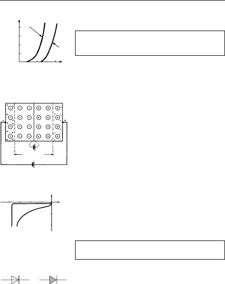
When an external voltage is applied to a p-n junction making the p-
type material positive with respect to the n-type material, as shown in
Figure 11.7, the p-n junction is forward biased. The applied voltage
opposes the contact potential, and, in effect, closes the depletion layer.
Holes and electrons can now cross the junction and a current flows.
Contact
potential
Applied
voltage
Depletion
layer
p-type
material
n-type
material
Figure 11.7
An increase in the applied voltage above that required to narrow the
depletion layer (about 0.2V for germanium and 0.6V for silicon), results
in a rapid rise in the current flow. Graphs depicting the current-voltage
relationship for forward biased p-n junctions, for both germanium and
silicon, called the forward characteristics, are shown in Figure 11.8.
When an external voltage is applied to a p-n junction making the
p-type material negative with respect to the n-type material as in shown
in Figure 11.9, the p-n junction is reverse biased. The applied voltage
is now in the same sense as the contact potential and opposes the move-
ment of holes and electrons due to opening up the depletion layer. Thus,
in theory, no current flows. However at normal room temperature certain
electrons in the covalent bond lattice acquire sufficient energy from the
heat available to leave the lattice, generating mobile electrons and holes.
This process is called electron-hole generation by thermal excitation.
The electrons in the p-type material and holes in the n-type material
caused by thermal excitation, are called minority carriers and these will
be attracted by the applied voltage. Thus, in practice, a small current
of a few microamperes for germanium and less than one microampere
for silicon, at normal room temperature, flows under reverse bias condi-
tions. Typical reverse characteristics are shown in Figure 11.10 for both
germanium and silicon.
11.6 Semiconductor
diodes
A semiconductor diode is a device having a p-n junction mounted in a
container, suitable for conducting and dissipating the heat generated in
operation, and having connecting leads. Its operating characteristics are as
shown in Figures 11.8 and 11.10. Two circuit diagram symbols for semi-
conductor diodes are in common use and are as shown in Figure 11.11.

Semiconductor diodes 141
Germanium
Silicon
0
10
20
30
40
0.2 0.4 0.6 0.8
Current
(mA)
Voltage (V)
Figure 11.8
Sometimes the symbols are encircled as shown in Figures 14.14–14.16
on pages 208 and 209.
Contact
potential
Depletion layer
p-type
material
n-type
material
Figure 11.9
−100 −75 −50 −25
−5
−10
Current
(µA)
Silicon
Germanium
Voltage (V)
Figure 11.10
Problem 1. Explain briefly the terms given below when they are
associated with a p-n junction: (a) conduction in intrinsic semicon-
ductors (b) majority and minority carriers, and (c) diffusion
(a) Silicon or germanium with no doping atoms added are called intrinsic
semiconductors. At room temperature, some of the electrons acquire
sufficient energy for them to break the covalent bond between atoms
and become free mobile electrons. This is called thermal generation
of electron-hole pairs. Electrons generated thermally create a gap in
the crystal structure called a hole, the atom associated with the hole
being positively charged, since it has lost an electron. This posi-
tive charge may attract another electron released from another atom,
creating a hole elsewhere.
When a potential is applied across the semiconductor material, holes
drift towards the negative terminal (unlike charges attract), and elec-
trons towards the positive terminal, and hence a small current flows.
(b) When additional mobile electrons are introduced by doping a
semiconductor material with pentavalent atoms (atoms having five
valency electrons), these mobile electrons are called majority
carriers. The relatively few holes in the n-type material produced
by intrinsic action are called minority carriers.
For p-type materials, the additional holes are introduced by doping
with trivalent atoms (atoms having three valency electrons). The
holes are apparently positive mobile charges and are majority carriers
in the p-type material. The relatively few mobile electrons in the
p-type material produced by intrinsic action are called minority
carriers.
(c) Mobile holes and electrons wander freely within the crystal lattice
of a semiconductor material. There are more free electrons in n-type
material than holes and more holes in p-type material than electrons.
Thus, in their random wanderings, on average, holes pass into the
n-type material and electrons into the p-type material. This process
is called diffusion.
Problem 2. Explain briefly why a junction between p-type and
n-type materials creates a contact potential.
Intrinsic semiconductors have resistive properties, in that when an applied
voltage across the material is reversed in polarity, a current of the same
magnitude flows in the opposite direction. When a p-n junction is formed,
the resistive property is replaced by a rectifying property, that is, current
passes more easily in one direction than the other.
Figure 11.11

142 Electrical Circuit Theory and Technology
An n-type material can be considered to be a stationary crystal matrix
of fixed positive charges together with a number of mobile negative
charge carriers (electrons). The total number of positive and negative
charges are equal. A p-type material can be considered to be a number of
stationary negative charges together with mobile positive charge carriers
(holes).
Again, the total number of positive and negative charges are equal
and the material is neither positively nor negatively charged. When the
materials are brought together, some of the mobile electrons in the n-type
material diffuse into the p-type material. Also, some of the mobile holes
in the p-type material diffuse into the n-type material.
Many of the majority carriers in the region of the junction combine
with the opposite carriers to complete covalent bonds and create a region
on either side of the junction with very few carriers. This region, called
the depletion layer, acts as an insulator and is in the order of 0.5
µm
thick. Since the n-type material has lost electrons, it becomes positively
charged. Also, the p-type material has lost holes and becomes negatively
charged, creating a potential across the junction, called the barrier or
contact potential.
Problem 3. Sketch the forward and reverse characteristics of a
silicon p-n junction diode and describe the shapes of the character-
istics drawn.
A typical characteristic for a silicon p-n junction having a forward bias is
shown in Figure 11.8 and having a reverse bias in Figure 11.10. When the
positive terminal of the battery is connected to the p-type material and the
negative terminal to the n-type material, the diode is forward biased. Due
to like charges repelling, the holes in the p-type material drift towards
the junction. Similarly the electrons in the n-type material are repelled by
the negative bias voltage and also drift towards the junction. The width
of the depletion layer and size of the contact potential are reduced. For
applied voltages from 0 to about 0.6V, very little current flows. At about
0.6V, majority carriers begin to cross the junction in large numbers and
current starts to flow. As the applied voltage is raised above 0.6 V, the
current increases exponentially (see Figure 11.8).
When the negative terminal of the battery is connected to the p-type
material and the positive terminal to the n-type material the diode is
reverse biased. The holes in the p-type material are attracted towards the
negative terminal and the electrons in the n-type material are attracted
towards the positive terminal (unlike charges attract). This drift increases
the magnitude of both the contact potential and the thickness of the deple-
tion layer, so that only very few majority carriers have sufficient energy
to surmount the junction.
The thermally excited minority carriers, however, can cross the junc-
tion since it is, in effect, forward biased for these carriers. The move-
ment of minority carriers results in a small constant current flowing.
As the magnitude of the reverse voltage is increased a point will be
reached where a large current suddenly starts to flow. The voltage at

Semiconductor diodes 143
Figure 11.12
which this occurs is called the breakdown voltage. This current is due to
two effects:
(i) the zener effect, resulting from the applied voltage being sufficient
to break some of the covalent bonds, and
(ii) the avalanche effect, resulting from the charge carriers moving at
sufficient speed to break covalent bonds by collision.
A zener diode is used for voltage reference purposes or for voltage stabil-
isation. Two common circuit diagram symbols for a zener diode are shown
in Figure 11.12.
11.7 Rectification
The process of obtaining unidirectional currents and voltages from alter-
nating currents and voltages is called rectification. Automatic switching
in circuits is carried out by diodes. For methods of half-wave and full-
wave rectification, see Section 14.7, page 208.
11.8 Further problems
on semiconductor diodes
1. Explain what you understand by the term intrinsic semiconductor
and how an intrinsic semiconductor is turned into either a p-type or
an n-type material.
2. Explain what is meant by minority and majority carriers in an n-type
material and state whether the numbers of each of these carriers are
affected by temperature.
3. A piece of pure silicon is doped with (a) pentavalent impurity and
(b) trivalent impurity. Explain the effect these impurities have on
the form of conduction in silicon.
4. With the aid of simple sketches, explain how pure germanium can
be treated in such a way that conduction is predominantly due to
(a) electrons and (b) holes.
5. Explain the terms given below when used in semiconductor
terminology: (a) covalent bond (b) trivalent impurity (c) pentavalent
impurity (d) electron-hole pair generation.
6. Explain briefly why although both p-type and n-type materials have
resistive properties when separate, they have rectifying properties
when a junction between them exists.
7. The application of an external voltage to a junction diode can influ-
ence the drift of holes and electrons. With the aid of diagrams
explain this statement and also how the direction and magnitude
of the applied voltage affects the depletion layer.
8. State briefly what you understand by the terms:
(a) reverse bias (b) forward bias (c) contact potential (d) diffusion
(e) minority carrier conduction.

144 Electrical Circuit Theory and Technology
9. Explain briefly the action of a p-n junction diode:
(a) on open-circuit, (b) when provided with a forward bias, and
(c) when provided with a reverse bias. Sketch the characteristic
curves for both forward and reverse bias conditions.
10. Draw a diagram illustrating the charge situation for an unbiased p-n
junction. Explain the change in the charge situation when compared
with that in isolated p-type and n-type materials. Mark on the
diagram the depletion layer and the majority carriers in each region.
