Alciatore D.G., Histand M.B. Introduction to Mechatronics and Measurement Systems
Подождите немного. Документ загружается.

Confirming Pages
many more video demonstrations of various music, sound, and vibration concepts,
see Internet Link 8.2.
8.2 QUANTIZING THEORY
Now we look at the process required to change a sampled analog voltage into digital
form. The process, called analog-to-digital conversion, conceptually involves two
steps: quantizing and coding. Quantizing is defined as the transformation of a con-
tinuous analog input into a set of discrete output states. Coding is the assignment of
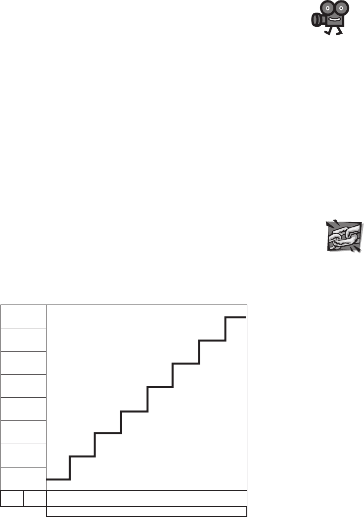
a digital code word or number to each output state. Figure 8.3 illustrates how a con-
tinuous voltage range is divided into discrete output states, each of which is assigned
a unique code. Each output state covers a subrange of the overall voltage range. The
stair-step signal represents the states of a digital signal generated by sampling a lin-
ear ramp of an analog signal occurring over the voltage range shown.
An analog-to-digital converter is an electronic device that converts an analog
voltage to a digital code. The output of the A/D converter can be directly interfaced
to digital devices such as microcontrollers and computers. The resolution of an A/D
converter is the number of bits used to digitally approximate the analog value of the
input. The number of possible states N is equal to the number of bit combinations
that can be output from the converter:
N = 2
n
(8.3)
where n is the number of bits. For the example illustrated in Figure 8.3 , the 3-bit
device has 2
3
or 8 output states as listed in the first column. The output states are
In
te
rn
et
Lin
k
8.2 Music,
sound, and
vibration
demonstrations
Figure 8.3 Analog-to-digital conversion.
7 111
6
110
5 101
4 100
3 011
2 010
1 001
0 000
output
state
output
code
0.00 –
1.25
1.25 –
2.50
2.50 –
3.75
3.75 –
5.00
5.00 –
6.25
6.25 –
7.50
7.50 –
8.75
8.75 –
10.0
discretized analog voltage ranges
8.4 Data
acquisition
experiment
8.5 LabVIEW data
acquisition and
music sampling
8.6 Sampling rate
and its effect on
sound and music
(audio only)
8.7 Music
sampling rate and
resolution effects
Video Demo
8.2 Quantizing Theory 351
alc80237_ch08_346-374.indd 351alc80237_ch08_346-374.indd 351 11/01/11 4:05 PM11/01/11 4:05 PM
Confirming Pages
352 CHAPTER 8 Data Acquisition
usually numbered consecutively from 0 to ( N ⫺ 1). The corresponding code word for
each output state is listed in the second column. Most commercial A/D converters are
8-, 10-, or 12-bit devices that resolve 256, 1024, and 4096 output states, respectively.
The number of analog decision points that occur in the process of quantizing is
( N ⫺ 1). In Figure 8.3 , the decision points occur at 1.25 V, 2.50 V, . . . , and 8.75 V.
The analog quantization size Q, sometimes called the code width, is defined as the
full-scale range of the A/D converter divided by the number of output states:
Q = (V
max
– V
min
) ⁄ N
(8.4)
It is a measure of the analog change that can be resolved by the converter. Although
the term resolution is defined as the number of output bits from an A/D converter,
sometimes it is used to refer to the analog quantization size. For our example, the
analog quantization size is 10/8 V ⫽ 1.25 V. This means that the amplitude of the
digitized signal has an error of at most 1.25 V. Therefore, the A/D converter can only
resolve a voltage to within 1.25 V of the exact analog voltage.
Video Demo 8.7 demonstrates how both sampling rate and A/D resolution affect
the fidelity of digitized music.
8.7 Music
sampling rate and
resolution effects
Video Demo
■ CLASS DISCUSSION ITEM 8.3
Laboratory A/D Conversion
Why is a 12-bit A/D converter satisfactory for most laboratory measurements?
8.3 ANALOG-TO-DIGITAL CONVERSION
8.3.1 Introduction
To properly acquire an analog voltage signal for digital processing, the following
components must be properly selected and applied in this sequence:
1 . buffer amplifier
2 . low-pass filter
3 . sample and hold amplifier
4 . analog-to-digital converter
5 . computer
The components required for A/D conversion along with an illustration of their
respective outputs are shown in Figure 8.4 . The buffer amplifier isolates the out-
put from the input (i.e., it draws negligible current and power from the input) and
provides a signal in a range close to but not exceeding the full input voltage range
of the A/D converter. The low-pass filter is necessary to remove any undesirable
high- frequency components in the signal that could produce aliasing. The cutoff fre-
quency of the low-pass filter should be no greater than 1/2 the sampling rate. The
sample and hold amplifier (see Section 5.12) maintains a fixed input value (from
an instantaneous sample) during the short conversion time of the A/D converter.
alc80237_ch08_346-374.indd 352alc80237_ch08_346-374.indd 352 11/01/11 4:05 PM11/01/11 4:05 PM
Confirming Pages
The converter should have a resolution and analog quantization size appropriate to
the system and signal. The computer must be properly interfaced to the A/D con-
verter system to store and process the data. The computer must also have sufficient
memory and permanent storage media to hold all of the data.
The A/D system components described above can be found packaged in a vari-
ety of commercial products called data acquisition (DAC or DAQ) cards or modules.
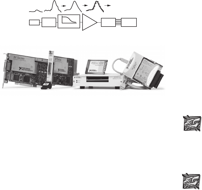
As shown in Figure 8.5 , DAC products are available in a variety of form factors
including PC and instrument panel plug-in cards, laptop computer PCMCIA cards,
and stand-alone external units with standard interfaces (e.g., USB). Internet Link 8.3
provides links to vendors and sources of information for various products available
on the market.
Data acquisition cards and modules usually support various high-level lan-
guage interfaces (e.g., C ⫹ ⫹ , Visual Basic, FORTRAN) that give easy access to the
product’s features. Easy-to-use software applications are also available to provide
graphical interfaces to program a DAC module to acquire, process, and output sig-
nals. National Instruments’ LabVIEW software is an example (see Internet Link 8.4
and Section 8.5 for more information). With a commercial DAC system, interfac-
ing signals between a mechatronic system or laboratory experiment and a desktop
computer is a simple matter of calling a function from a custom-written program or
clicking and dragging icons in a graphical interface. Lab Exercise 12 explores the
basics of how to use the LabVIEW software to sample and store an external voltage
signal, including sampled music. Video Demo 8.5 demonstrates all of the steps in the
process, and Section 8.6 explores the details.
In addition to A/D converters, commercial DAC systems usually provide
other input and output functionality including binary (TTL-compatible) I/O, D/A
buffer
amplifier
sample
& hold
low-pass filter
0011 0010 0100
0011 0010 1011
0011 0011 1100
0011 0101 0111
: : :
: : :
A/D
converter
computer/
memory
sensor
Figure 8.4 Components used in A/D conversion.
In
te
rn
et
Lin
k
8.3 Data
acquisition online
resources and
vendors
In
te
rn
et
Lin
k
8.4 National
Instruments’
LabVIEW software
Figure 8.5 Various form factors of data acquisition products. ( Courtesy of National
Instruments, Austin, TX )
8.3 Analog-to-Digital Conversion 353
alc80237_ch08_346-374.indd 353alc80237_ch08_346-374.indd 353 11/01/11 4:05 PM11/01/11 4:05 PM
Confirming Pages
Lab Exercise
Lab 12 Data
acquisition
354 CHAPTER 8 Data Acquisition
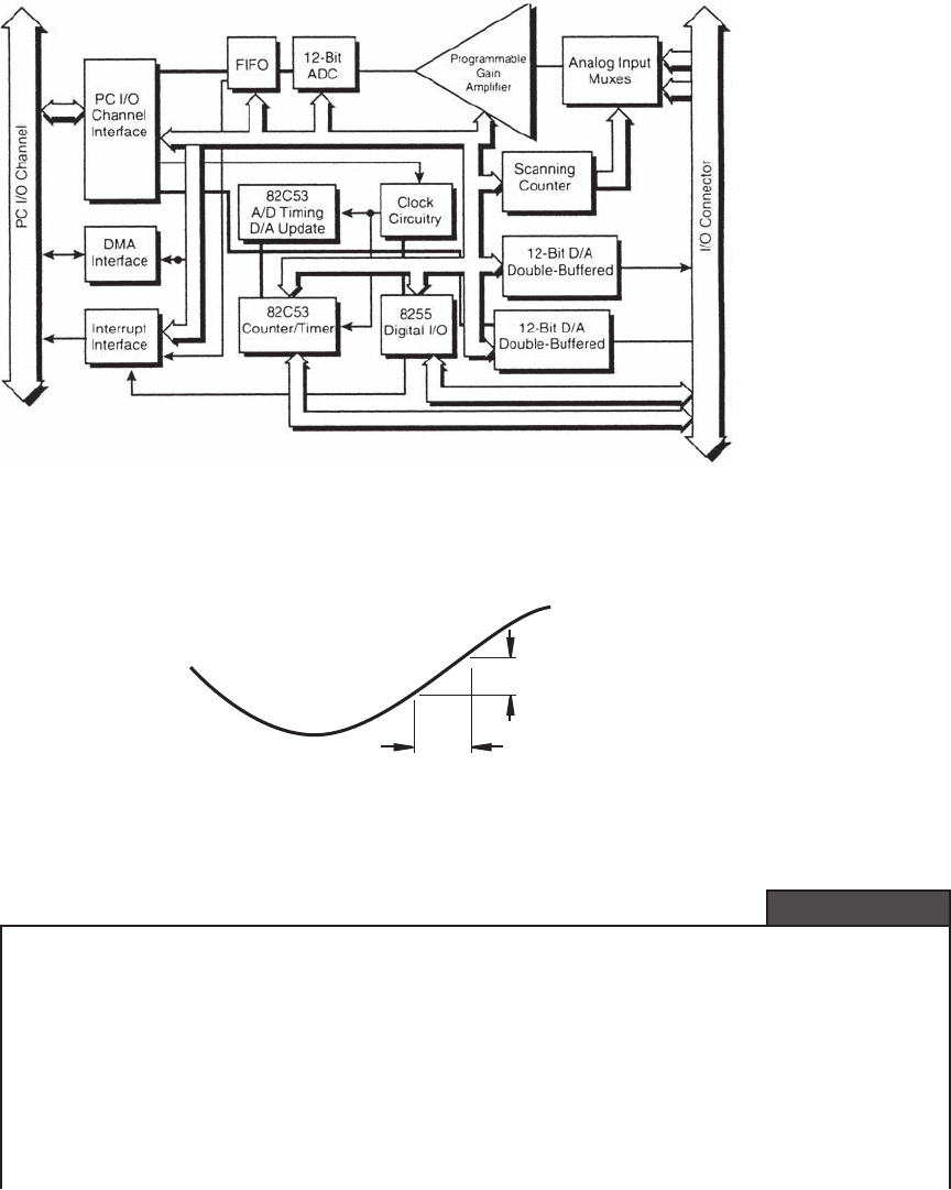
converters, counters and timers, and signal conditioning circuitry. Important features
when selecting a DAC system include the A/D and D/A resolutions (the number of
bits used) and the maximum sampling rate supported. These features are key to accu-
racy and reliability in computer monitoring and control applications. An example
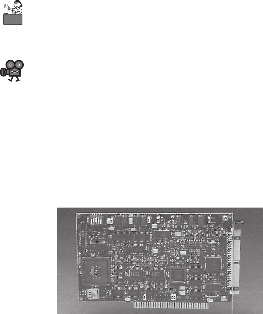
data acquisition and control card that can be inserted into a PC motherboard slot is
shown in Figure 8.6 . Its internal architecture is illustrated in Figure 8.7 . The card’s
functions include two 12-bit D/A converters, one 12-bit A/D converter, 24 lines of
digital I/O, and three 16-bit counter-timers.
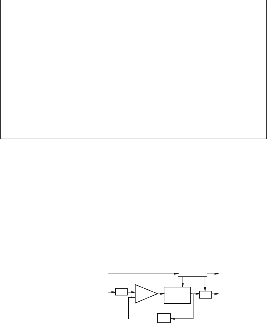
The process of analog-to-digital conversion requires a small but finite interval
of time that must be taken into consideration when assessing the accuracy of the
results. The conversion time, also called settling time, depends on the design of the
converter, the method used for conversion, and the speed of the components used in
the electronic design. Because analog signals change continuously, the uncertainty
about when in the sample time window the conversion occurs causes corresponding
uncertainty in the digital value. This is of particular concern if there is no sample and
hold amplifier on the A/D input. The term aperture time refers to the duration of the
time window and is associated with any error in the digital output due to changes in
the input during this time. The relationship between the aperture time and the uncer-
tainty in the input amplitude is shown in Figure 8.8 . During the aperture time Δ T
a
,
the input signal changes by Δ V, where
ΔV
dVt()
dt
-------------
ΔT
a
≈
(8.5)
Sampling at or above the Nyquist frequency will yield the correct frequency
components in a signal. However, to also obtain accurate amplitude resolution, we
must have an A/D converter with a sufficiently small aperture time. It is often in the
nanosecond range for 10- and 12-bit resolution.
8.5 LabVIEW data
acquisition and
music sampling
Video Demo
Figure 8.6 Example data acquisition and control card. (Courtesy of National
Instruments, Austin, TX)
alc80237_ch08_346-374.indd 354alc80237_ch08_346-374.indd 354 11/01/11 4:05 PM11/01/11 4:05 PM
Confirming Pages
Figure 8.7 Example data acquisition and control card architecture. (Courtesy of
National Instruments, Austin, TX)
ΔT
a
ΔV
V(t)
Figure 8.8 A/D conversion aperture time.
Aperture Time
EXAMPLE 8.2
Consider a sinusoidal signal A sin( t ) as an input to an A/D converter. The time rate of
change of the signal A cos( t ) has a maximum value of A . Using Equation 8.5 , the maxi-
mum change in the input voltage during an aperture time Δ T
a
is
ΔVAωΔT
a
=
To eliminate uncertainty in the value of the digital output, we need to ensure that Δ V is less
than the analog quantization size:
ΔV
2A
N
------ -
<
(continued )
8.3 Analog-to-Digital Conversion 355
alc80237_ch08_346-374.indd 355alc80237_ch08_346-374.indd 355 11/01/11 4:05 PM11/01/11 4:05 PM
Confirming Pages
356 CHAPTER 8 Data Acquisition
8.3.2 Analog-to-Digital Converters
A/D converters are designed based on a number of different principles: successive
approximation, flash or parallel encoding, single-slope and dual-slope integration,
switched capacitor, and delta sigma. We consider the first two because they occur
most often in commercial designs. The successive approximation A/D converter
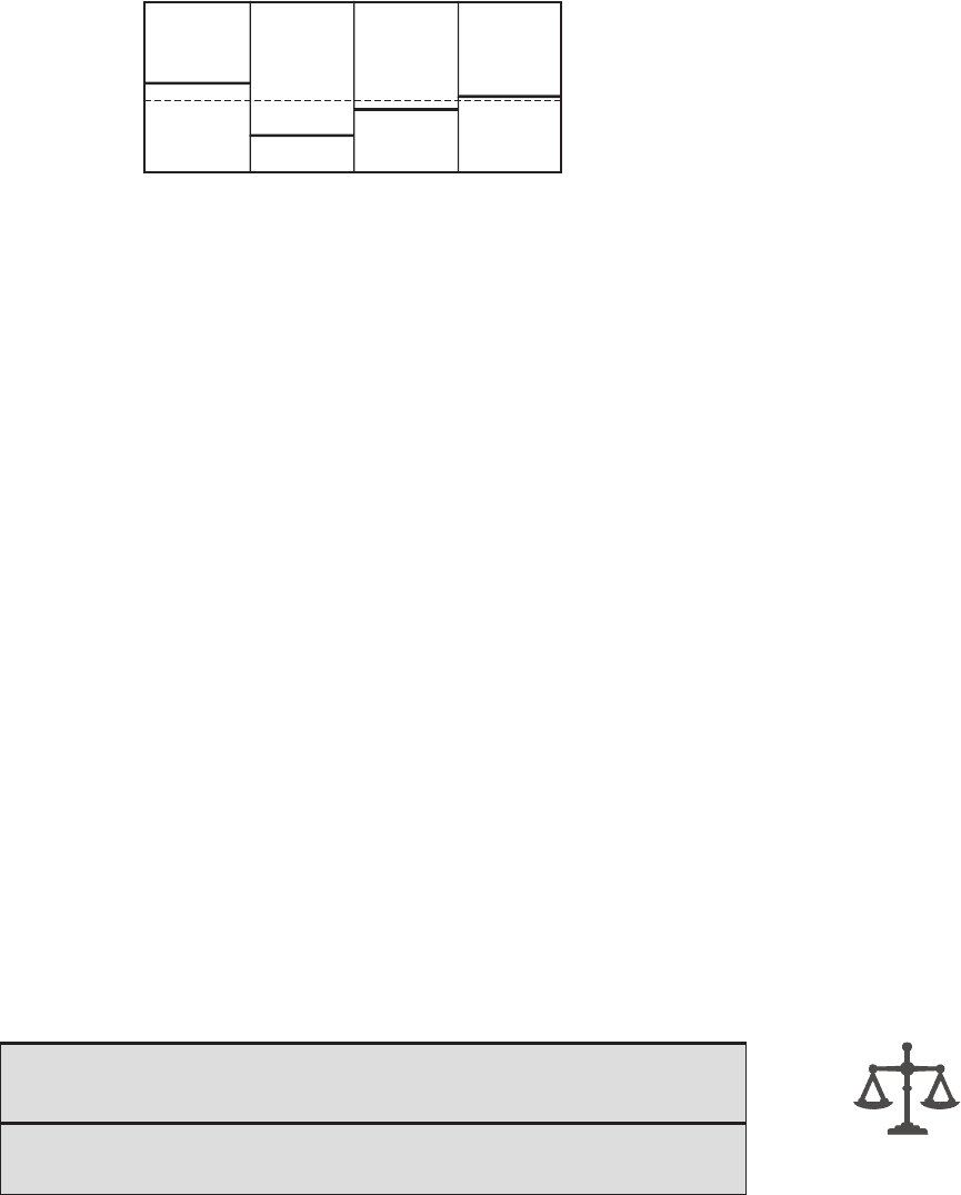
is very widely used because it is relatively fast and cheap. As shown in Figure 8.9 ,
it uses a D/A converter in a feedback loop. D/A converters are described in the
next section. When the start signal is applied, the sample and hold (S&H) amplifier
latches the analog input. Then the control unit begins an iterative process, where the
digital value is approximated, converted to an analog value with the D/A converter,
and compared to the analog input with the comparator. When the D/A output equals
the analog input, the end signal is set by the control unit, and the correct digital out-
put is available at the output.
where 2 A is the total voltage range and N is the number of output states. At the limit of this
constraint,
ΔV
2A
N
------ -
=
Therefore, the required aperture time, if a sample and hold amplifier is not being used, is
ΔT
a
ΔV
Aω
--------
2
Nω
--------
==
Consider, for example, converting a signal using 10-bit resolution, which provides
2
10
(1024) output states. If the signal were speech (from a microphone) with a bandwidth of
10 kHz,
Δ T
a
would have to be less than
ΔT
a
2
Nω
--------
2
1024 2π 10,000⋅()
---------------------------------------------
3.2 10
8–
× 32 nsec== = =
This is a very short required aperture time compared to the required minimum sample period
given by 1/[2(10 kHz)] ⫽ 50 sec. Even for this low-resolution converter, the required aper-
ture time (32 nsec) is much smaller than the required sample period (50,000 nsec).
(continued )
analog
input
D/A
digital
output
S&H
comparator
successive
approximation
register
latch
control unit
start
signal
end
signal
Figure 8.9 Successive approximation A/D converter.
alc80237_ch08_346-374.indd 356alc80237_ch08_346-374.indd 356 11/01/11 4:05 PM11/01/11 4:05 PM
Confirming Pages
If n is the resolution of the A/D converter, it takes n steps to complete the con-
version. More specifically, the input is compared to combinations of binary fractions
(1/2, 1/4, 1/8, . . . , 1/2
n
) of the full-scale (FS) value of the A/D converter. The control
unit first turns on the most significant bit (MSB) of the register, leaving all lesser bits
at 0, and the comparator tests the DAC output against the analog input. If the analog
input exceeds the DAC output, the MSB is left on (high); otherwise, it is reset to 0.
This procedure is then applied to the next lesser significant bit and the comparison
is made again. After n comparisons have occurred, the converter is down to the least
significant bit (LSB). The output of the DAC then represents the best digital approxi-
mation to the analog input. When the process terminates, the control unit sets the end
signal signifying the end of the conversion.
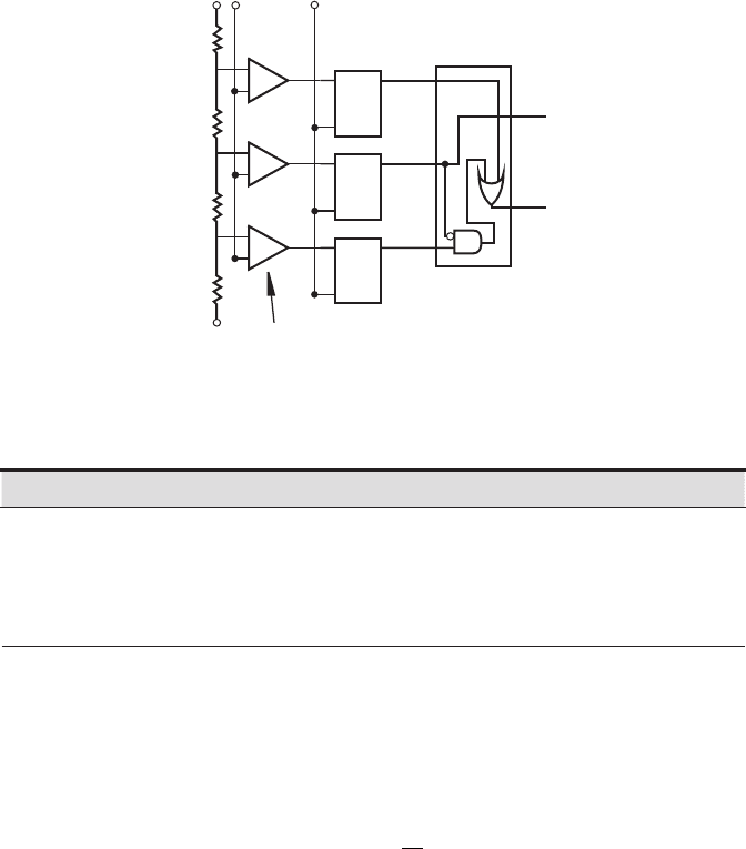
As an example, a 4-bit successive approximation procedure is illustrated graphi-
cally in Figure 8.10 . The MSB is 1/2 FS, which in this case is greater than the signal;
therefore, the bit is turned off. The second bit is 1/4 FS and is less than the signal,
so it is left on. The third bit gives 1/4 ⫹ 1/8 of FS, which is still less than the analog
signal, so the third bit is left on. The fourth provides 1/4 ⫹ 1/8 ⫹ 1/16 of FS and is
greater than the signal, so the fourth bit is turned off and the conversion is complete.
The digital result is 0110. Higher resolution would produce a more accurate value.
An n -bit successive approximation A/D converter has a conversion time of n Δ T,
where Δ T is the cycle time for the D/A converter and control unit. Typical conversion
times for 8-, 10-, and 12-bit successive approximation A/D converters range from
1 to 100 s.
The fastest type of A/D converter is known as a flash converter. As Figure 8.11
illustrates, it consists of a bank of input comparators acting in parallel to identify
the signal level. The output of the latches is in a coded form easily converted to the
required binary output with combinational logic. The flash converter illustrated in
Figure 8.11 is a 2-bit converter having a resolution of four output states. Table 8.1
input
signal
0
011
21
0
FS
1/2 FS
bit
3 (MSB) 0 (LSB)
1/4 FS
(1/4 + 1/8) FS
Figure 8.10 4-bit successive approximation A/D conversion.
■ CLASS DISCUSSION ITEM 8.4
Selecting an A/D Converter
What are some reasons why a designer might select a 10-bit A/D converter instead
of a 12-bit or higher resolution converter?
8.3 Analog-to-Digital Conversion 357
alc80237_ch08_346-374.indd 357alc80237_ch08_346-374.indd 357 11/01/11 4:05 PM11/01/11 4:05 PM
Confirming Pages
358 CHAPTER 8 Data Acquisition
lists the comparator output codes and corresponding binary outputs for each of the
states, assuming an input voltage range of 0 to 4 V. The voltage range is set by the
V
min
and V
max
supply voltages shown in Figure 8.11 (0 V and 4 V in this example).
The code converter is a simple combinational logic circuit. For the 2-bit converter,
the relationships between the code bits G
i
and the binary bits B
i
( Question 8.11 ) are
B
0
G
0
G
1
G
2
+⋅=
(8.6)
B
1
G
1
=
(8.7)
Adding more resolution is a simple matter of adding more resistors, comparators,
and latches. The combinational logic code converter would also be different. Unlike
with the successive approximation converter, adding resolution does not increase the
time required for a conversion.
Several analog signals can be digitized by a single A/D converter if the analog
signals are multiplexed at the input to the A/D converter. An analog multiplexer
simply switches among several analog inputs using transistors or relays and control
signals. This can significantly reduce the cost of a system’s design. In addition to
cost, other parameters important in selecting an A/D converter are the input voltage
range, output resolution, and conversion time.
–
+
Q
D
C
–
+
Q
D
C
–
+
Q
D
C
code
converter
V
max
V
in
V
min
R
R
R
R
trigger
comparators
latches
G
2
B
1
B
0
G
1
G
0
Figure 8.11 A/D flash converter.
Table 8.1 2-bit flash converter output
State Code (G
2
G
1
G
0
) Binary (B
1
B
0
) Voltage Range
0 000 00 0–1
1 001 01 1–2
2 011 10 2–3
3 111 11 3–4
alc80237_ch08_346-374.indd 358alc80237_ch08_346-374.indd 358 11/01/11 4:05 PM11/01/11 4:05 PM
Confirming Pages
8.4 DIGITAL-TO-ANALOG CONVERSION
Often we need to reverse the process of A/D conversion by changing a digital value
to an analog voltage. This is called digital-to-analog (D/A) conversion. A D/A con-
verter allows a computer or other digital device to interface with external analog
circuits and devices.
The simplest type of D/A converter is a resistor ladder network connected to an
inverting summer op amp circuit as shown in Figure 8.12 . This particular converter is a
4-bit R -2 R resistor ladder network, which requires only two precision resistance values
( R and 2 R ). The digital input to the DAC is a 4-bit binary number represented by bits
b
0
, b
1
, b
2
, and b
3
, where b
0
is the least significant bit and b
3
is the most significant bit.
Each bit in the circuit controls a switch between ground and the inverting input of the
op amp. To understand how the analog output voltage V
out
is related to the input binary
number, we can analyze the four different input combinations 0001, 0010, 0100, and
1000 and apply the principle of superposition for an arbitrary 4-bit binary number.
If the binary number is 0001, the b
0
switch is connected to the op amp, and the
other bit switches are grounded. The resulting circuit is as shown in Figure 8.13 .
Because the noninverting input of the op amp is grounded, the inverting input is also
at ground. The equivalent resistance between node V
0
and ground is R, which is the
parallel combination of two 2 R values. Therefore, V
0
is the result of voltage division
of V
1
across two series resistors of equal value R:
V
0
1
2
-- -
V
1
=
(8.8)
–
+
2R
R
2R 2R 2R
MSB LSB
V
s
V
out
2R
RRR
b
3
b
2
b
1
b
0
Figure 8.12 4-bit resistor ladder D/A converter.
Figure 8.13 4-bit resistor ladder D/A with digital input 0001.
–
+
2R
2R
R
b
3
b
2
b
1
b
0
2R
R
2R
R
2R
R
V
s
V
3
V
2
V
1
V
0
V
out
0
8.4 Digital-to-Analog Conversion 359
alc80237_ch08_346-374.indd 359alc80237_ch08_346-374.indd 359 11/01/11 4:05 PM11/01/11 4:05 PM
Confirming Pages
360 CHAPTER 8 Data Acquisition
Similarly, we can show that
andV
1
1
2
-- -
V
2
= V
2
1
2
-- -
V
3
=
(8.9)
Therefore,
V
0
1
8
-- -
V
3
1
8
-- -
V
s
==
(8.10)
V
0
is the input to the inverting amplifier circuit, which has a gain of
R
2R
------ -
–
1
2
-- -
–=
( 8.11)
Therefore, the analog output voltage corresponding to the binary input 0001 is
V
out
0
1
16
----- -
V
s
–=
(8.12)
Similarly, we can show ( Questions 8.16 through 8.18 ) that, for the input 0010,
V
out
1
1
8
-- -
V
s
–=
(8.13)
and for the input 0100,
V
out
2
1
4
-- -
V
s
–=
(8.14)
and for the input 1000,
V
out
3
1
2
-- -
V
s
–=
(8.15)
The output for any combination of bits comprising the input binary number can now
be found using the principle of superposition:
V
out
b
3
V
out
3
b
2
V
out
2
b
1
V
out
1
b
0
V
out
0
+++=
(8.16)
If V
s
is 10 V, the output ranges from 0 V to ( ⫺ 15/16)10 V for the 4-bit binary
input, which has 16 values ranging from 0000 (0) to 1111 (15). A negative ref-
erence voltage V
s
can be used to produce a positive output voltage range. Either
case yields a unipolar output, which is either positive or negative but not both.
A bipolar output, which ranges over negative and positive values, can be produced
by replacing all ground references in the circuit with a reference voltage whose sign
is opposite to V
s
.
alc80237_ch08_346-374.indd 360alc80237_ch08_346-374.indd 360 11/01/11 4:05 PM11/01/11 4:05 PM
