Valery Vodovozov, Raik Jansikene. Power Electronic Converters
Подождите немного. Документ загружается.

61
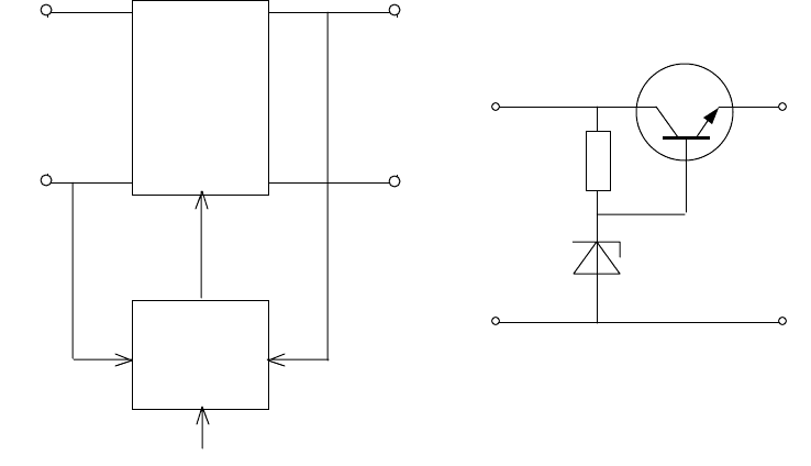
Fig. 4.1 Fig. 4.2
The Zener diode D establishes the bias voltage placed on the base of the transistor. For this
purpose, the resistor R
1
senses voltage variations across the dc output U
out
caused by
changing U
in
. When this circuit is operated properly, if the voltage U
out
across the load in-
creases, the rise in emitter voltage makes the base less positive. The current through the
transistor will then be reduced, which results in the increase in the collector-emitter resis-
tance. This increase in resistance will cause a larger voltage drop across the transistor,
which will in turn compensate for the change in voltage across the load. Opposite conditions
would occur if the load voltage were to decrease. Here, the transistor dissipation is greatest
when the load current is maximal.
Since the ripple is equivalent to a periodic change in the output voltage, therefore, a voltage
regulator degenerates the ripple that comes in with the unregulated input voltage. The ripple
rejection U
r(in)
/ U
r(out)
is normally 10000 or more. Many variations of this circuit are used in
regulated power supply today. A number of pass devices may employ within voltage regula-
tor circuits – single npn and single pnp transistors, Darlington npn pairs, and MOSFET de-
vices.
There are two components to power, which are dissipated in the regulator; one is a function
of U
in
– U
out
and load current, plus a second, which is a function of U
in
and grounding current.
Obviously, the magnitude of the load current and the regulator dropout voltage both greatly
influence the power dissipation. The second term, usually only becomes significant when the
regulator is unloaded, and the converter’s quiescent power then produces a constant drain
on the source U
in
. However, it should be noted that in some types of regulators the ground
current under load could actually run quite high. This effect is worst at the onset of regula-
tion, or when the pass transistor is in saturation, and can be noted by a sudden ground cur-
rent spike, where the current jumps upward abruptly from the low level.
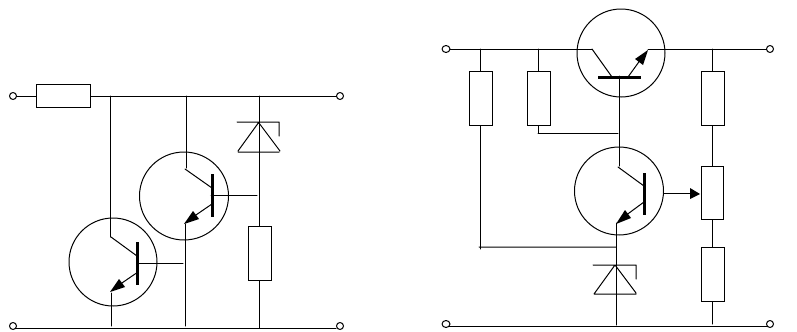
Shunt voltage regulator. The circuit of Fig 4.3 is a shunt voltage regulator sometimes
known as amplified Zener. Again, the Zener diode D is used to establish a constant bias
U
out
+
–
D
R
T
U
in
Reference
Feed-
back
Feed-
forward
Control
Power
converter
Controller
Power
input
Power
output
62
level. Therefore, only the resistor R
1
will sense voltage variations across the dc output U
out
. If
the output voltage U
out
rises, an increased positive voltage will be present at the base of the
transistor T
1
. The increased forward bias on T
1
will cause it to conduct more, which makes
the base of the transistor T
2
more positive. Transistor T
2
will conduct more heavily. In-
creased current flow through both transistors causes an increase in the voltage drop across
R
1
, which will then counterbalance the rise in output voltage U
out
. Thus, the direct output
voltage will remain stabilized. Decreases in the direct output voltage will cause the circuit
action to reverse. Shunt transistor voltage regulators are used extensively in independent
power supplies. Here, the transistor’s dissipation is greatest when the load current is least.
Compound voltage regulator. Fig. 4.4 illustrates a compound voltage regulator. Full load
current passes through the pass transistor T
2
. A voltage divider samples the output voltage
U
out
and delivers a feedback voltage to the base of T
1
. Any change in output voltage produce
an error voltage that automatically compensates for the attempted change. For instance, if
U
out
tries to increase, more feedback voltage is fed back to the base of T
1
, producing a larger
T
1
collector current through R
3
and less base voltage at T
2
. The reduced base voltage of T
2
emitter follower results in less output voltage. Similarly, if the output voltage tries to de-
crease, there is less base voltage at T
1
, more base voltage at T
2
, and more output voltage.
Fig. 4.3 Fig. 4.4
Because of the closed-loop voltage gain K = (R
1
+ R
2
) / R
1
, one can use a low Zener voltage
(about –4V) where the temperature coefficient approaches zero. The amplified output volt-
age then has the same temperature coefficient. The potentiometer allows adjusting the out-
put voltage to the exact value required in a particular application. As a result, U
out
remains
constant, despite changes in the line voltage or load current.
Summary. The linear converters offer the designer four major advantages:
• simplicity and low cost,
• quiet operation and load-handling capacity,
• little or no electrical noise on output,
• very short load response time.
U
out
+
–
R
s
D
R
1
T
1
T
2
U
in
T
2
–
+
R
D
R
3
R
2
R
1
T
1
U
out
U
in
63
For these good features, linear regulators have been valuable system components since the
early days. But the disadvantages of the linear-type regulators are what limit their range of
application:
• they can be used only for a step-down regulation,
• in off-line applications, a transformer with rectification and filtering must be placed
before them,
• each linear regulator can have only one output,
• low efficiency of 30 to 60% in normal applications results in headroom loss in the
transistor.
Because of this, linear regulators tend to get bulky at power applications.
4.2. Step-Down Choppers
Choppers. The switching supply is a much more versatile choice, with a wider range
of applications than the linear regulators. The main functions of choppers or switching dc
converters are:
• voltage levels changing,
• galvanic disconnection of electronic circuits providing,
• output voltage stabilizing.
Choppers circumvent most of the linear regulator’s shortcomings:
• exhibit efficiencies of 65 to 90% regardless of the output voltage, thus drastically
reducing the size requirement of the heat sink,
• since high frequency of operation, the magnetic and capacitive elements used for
energy storage are small and the cost of switching supply becomes less than the
linear regulator,
• output voltage can vary above and and/or below the level of the input voltage,
• when input voltage is chopped into an ac waveform and placed into magnetic
element, additional windings can be added to provide for more than one output
voltage.
The disadvantages of the switching converters are minor:
• more complication,
• considerable noise on its output and input that they radiate into the environment,
• considerable slow transient response time that they take to respond to changes
in the load due to time-limited pulses of energy.
The basic converter’s topologies are step-down and step-up.
Two basic modes of operation constitute the foundation of all choppers. These result in for-
ward-mode operation and flyback-mode operation. Both classes have as their functional
components four elements:
• a power switch,
• a rectifier (catch diode),
64
• an inductor,
• a capacitor.
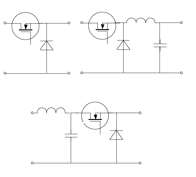
Single-quadrant forward choppers. In step-down forward chopper, the power switch T is
placed directly between the input voltage source U
in
and the load (Fig. 4.5, a) or before the
filter section (Fig. 4.5, b). The switch can be a conventional SCR, a GTO thyristor, or a tran-
sistor (MOSFET, IGBT, etc). It serves only to replenish the energy lost to the load during its
off time. If the switch is a GTO thyristor, a positive gate pulse will turn it on and a negative
gate pulse will turn it off. When a transistor switches, the base current or gate voltage con-
trols the on and off periods of the switch. If the switch is an SCR, a commutation circuit is
required to turn it off.
Fig. 4.5
The shunt (flywheel) diode D, series inductor L, and shunt capacitor C form an energy stor-
age reservoir whose purpose is to store enough energy to maintain the load current over the
entire off-time of the switch.
Usually, the output voltage is changed with the switch by PWM; therefore the voltage applied
to the load has the form of a square wave of varying periodicity (Fig. 4.6, a). The operation
of the forward converter can be broken up into two phases. The first is when the switch is
on. During this period, the current passes from the input source through the inductor to the
load. Diode is reverse-biased in this period. After the switch turns off, the inductor still ex-
pects current to flow through it. The diode now begins to conduct and the load current free-
wheels through the diode, thus maintaining a closed current loop through the load. Then the
switch is turned on again and the cycle repeats. Note that the output voltage is a chopped
voltage derived from the supply voltage, hence the name “chopper”.
T
+
–
D
a.
U
in
U
out
+
–
D
T L
C
b.
U
in
U
out
+
–
D
T L
C
c.
U
in
U
out

65
Fig. 4.6
By such a way, the load current fluctuates in magnitude as shown in Fig. 4.6, a, but is likely
to be continuous. With low inductance, the load current may fall to zero during the off peri-
ods of the switch (dotted lines in Fig. 4.6, a). The chopped source current makes the peak
input power demand high. Also, the supply current has harmonics, which produce voltage
fluctuations, signal interference, etc. LC input filter (Fig. 4.5, c) will provide a path for the rip-
ple current such that only the average current is drawn from the supply. The resonance fre-
quency of the filter is:
f
c
= 1 / (2π√(LC)),
thus to avoid resonance the chopped frequency should be f
ch
> (2 – 3)f
c
.
Duty cycle. Let the repetition period T = t
on
+ t
off
be designated as 2π radians. Since the in-
dependent variable is chosen as ωt, the periodic time of the overall cycle is 2π / ω. The fre-
quency of the chopper operation is the inverse of the periodic time, f
c
= ω / (2π). Typical
chopping frequencies are usually in the range 100 < f
c
< 1000 Hz for thyristor choppers and
up to 20 kHz for transistor choppers. In low power applications, MOSFET switches can be
used of frequencies in excess of 200 kHz. The on period of the chopper
t
on
= qT = 2πq,
where q is the duty cycle. The terms T
on,
T
off
now serve the double purpose of identifying the
construction state of switch and also defining its period of conduction in radians. Therefore,
q = t
on
/ T
where t
on
is the pulse width and T is the PWM cycle. The time mean value of the output volt-
age assuming continuous current mode is given by:
U
out
= qU
in
,
hence the output voltage varies linearly with the duty cycle of the chopper, as show continu-
ous traces in Fig. 4.6, b. dotted traces describe continuous current mode. If the load resis-
tance is R and the rated load current is I, then the mean value of the voltage should be RI,
therefore
q = RI / U
in
.
The turn-on time duration
t
on
= q / f
c
.
The rms value of the load voltage waveform is given by
U
out rms
=√q⋅U
in
.
t
t
off
t
on
I
out
U,I
U
out
a.
q=0,1
q=1
b
U
out
I
out
66
The ripple factor defining the ratio of the ac components to the average value is given by
r = √((1 – q) / q).
For full conduction q = 1 and r = 0.
Tw o-quadrant forw ard chopper. The previous circuit is only capable of supplying unidirec-
tional current and voltage to the load. Industrial applications of this circuit are normally lim-
ited to loads below 5 kW. Traction applications, however, are designed at ratings of hun-
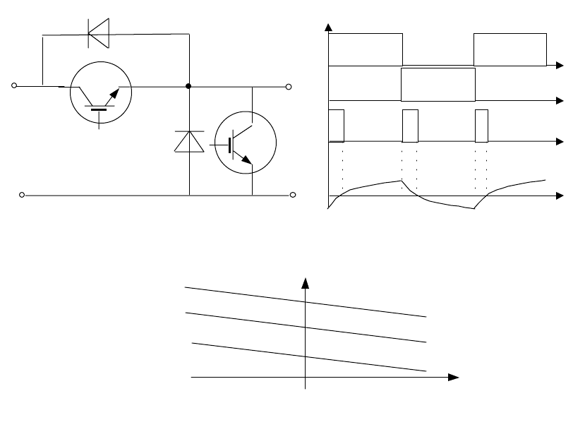
dreds kilowatt. A circuit that is capable of two-quadrant operation is shown in Fig. 4.7, a.
During the first phase, the converter operates as the basic chopper with T
1
and D
2
carrying
the current. The current flows through the load while the transistor T
1
is in on state.
Fig. 4.7
When the transistor T
1
is in off state, the reactive energy of the load dissipates through the
discharge transistor T
2
. During the second phase, T
1
is inoperative and T
2
controls the cur-
rent, which builds up negatively, limited by the load inductance. When T
2
turns off, the only
path for the current is via D
1
back into the supply; hence the circuit is regenerative (Fig.
4.7, b).Thus, this converter is able to reverse the current flow of the load but unable to re-
verse the load terminal voltage as show the load curve in Fig. 4.7, c.
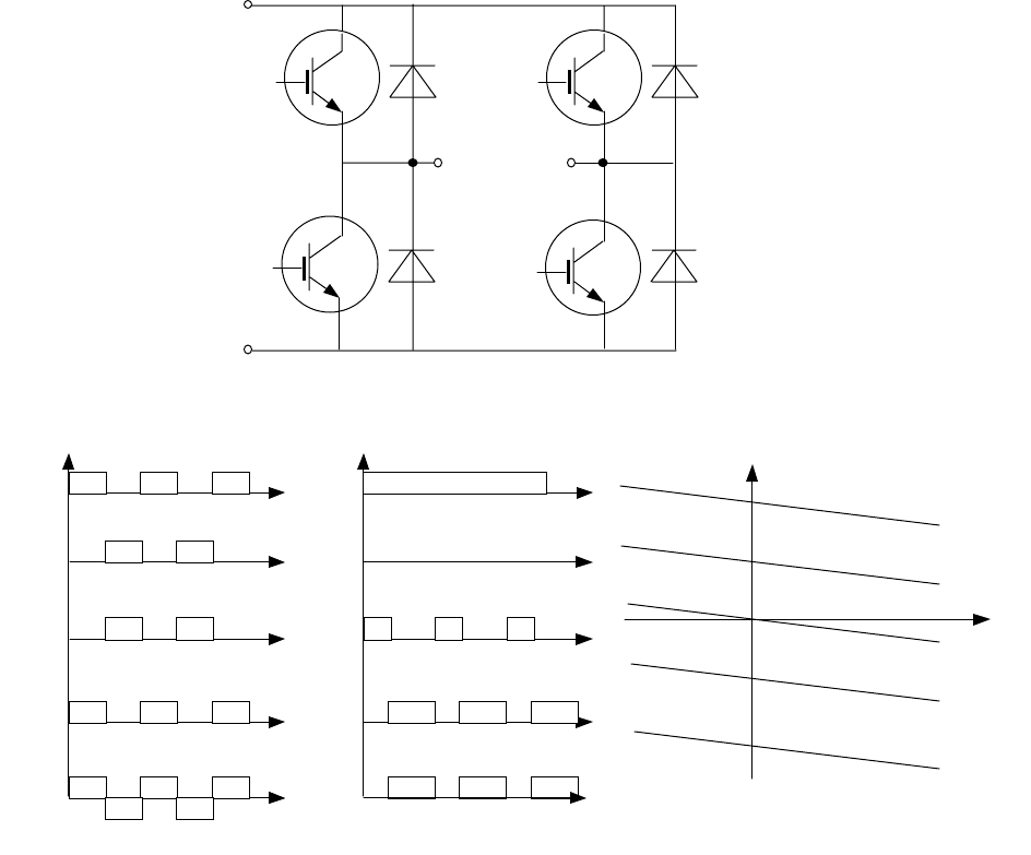
Four-quadrant forw ard chopper. Fig. 4.8, a shows a basic four-quadrant forward con-
verter. There are the two control methods of the bi-directional circuit shown in Fig. 4.8, a: a
symmetrical control and an asymmetrical control (Fig. 4.8, b).
When the symmetrical control is used, the four switches change their state simultaneously.
During the first phase, positive output transistors T
1
and T
4
are switched on in the on period
I
out
ωt
U,I
ωt
b.
ωt
D
2
q=0,1
q=1
I
out
c.
U
out
D
2
D
1
U
ou
t
–
+
T
2
a.
T
1
U
in
T
1
T
2
D
1
D
1
67
and diodes D
2
and D
4
conduct in the off period. When D
2
and D
4
conduct, the load supply is
reversed. Consequently, the voltage is reduced to zero at 0,5 duty cycle. Any reduction of
duty cycle below 0,5 will cause the output voltage to reverse but the current may save the
same direction; hence the load is regenerating. If the pulse length is less than the half pe-
riod, there is a negative voltage on the load. If the pulse length is more than the half period,
there is a positive voltage on the load. With transistors T
2
and T
3
conducting, the current is
reversed and hence the full four-quadrant operation is obtained as show the load curves Fig.
4.8, c. The disadvantage of the method is that amplitude of the output ripple voltage is twice
that of the simple converter, and the current ripple is therefore worse due to a high ripple
factor. This problem can be overcome by a technique known as the asymmetrical control. If
the load is resistive-inductive, the asymmetrical control is preferable. In this mode, the
switches T
3
and T
4
change their state while the switch T
1
is open and the switch T
2
is closed.
By such a way, when the switches change their state the current transfer is smoothed.
Fig. 4.8
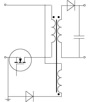
Transformer-isolated forward chopper. In between the switch and the filter section there
may be a transformer for stepping up or down the voltage as shown in Fig. 4.9. The trans-
former-isolated forward converter, again, passes the energy when the switch is on and the
operation cycle includes two phases: the working phase and the loose running. In the first
phase, the primary current flows through the closed switch, built on MOSFET and induces
I
out
–
+
Symmetrical control Asymmetrical control
t
t
t
t
t
t
t
t
t
T
2
T
3
T
4
U
out
T
1
T
2
T
3
T
4
U
out
T
1
U
in
T
4
T
3
T
2
T
1
U
out
a.
b.
q = 0,5
q = 0
q = 1
c.
U
out
68
the current in the secondary winding of the transformer. The secondary current charges the
capacitor. In the second phase, the diode is reverse biased due to the self-induction of a
transformer. Therefore, the load current occurs only because of the discharge of the capaci-
tor.
When the switch turns off, there is no full energy discharge of the transformer and the over-
voltage may occur in the windings. To prevent the overvoltage, the additional winding with a
diode is commonly used. The mass and weight of such transformer is growing up; it is the
main drawback of the forward circuit. The amount of energy being delivered to the load is
controlled by the duty cycle of the power switch on-time period. This may vary anywhere be-
tween 0 and 1 duty cycle and typically falls between 0,05 and 0,95. For light loads assume
approximately:
U
out
= qU
in
.
Fig. 4.9
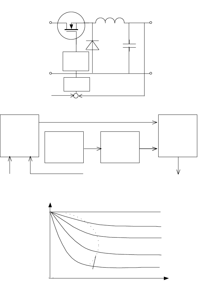
Buck regulator. A buck regulator is a forward converter with a feedback. In Fig. 4.10, a, the
regulator has a unidirectional current and one voltage polarity that allows controlling the out-
put voltage below the input supply voltage. Therefore, it is called a step-down regulator. The
series-pass transistor T in this circuit responds as a switch. Usually, this is done by control-
ling the duty cycle of the switching. The dc output has a square-wave characteristic. Then,
chopped dc feeds into the load.
The PWM controller, presented in Fig. 4.10, b adjusts the duty cycle to commit required ac-
tions to keep the output voltage at a desired level. Thanks to the negative voltage feedback,
the regulator does not allow the pass transistor to operate in the active region. Instead, it
alternately saturates and cuts off the pass transistor. This results in low power dissipation in
the transistor.
A sensing circuit that detects a change of the output voltage controls operation of the switch-
ing regulator. An increase in the power supply load, caused by a decrease in load resis-
tance, normally reduces the output voltage. A decrease in voltage causes an increase in the
PWM frequency. The PWM output is then applied to the gate of the transistor over the gate
driver. An increase in a gate frequency causes a corresponding increase in the chopper out-
+
–
U
out
U
in
69
put. This causes an increase in dc output to compensate for the change in load. A decrease
in the load normally raises the output voltage.
To compensate for this, the sensor detects the increased output voltage. An increase in out-
put voltage causes a decrease in PWM frequency. This causes a decrease in chopping rate.
Lower frequency causes a corresponding regulation in dc output. In a sense, the dc output is
regulated by the value of its chopping frequency. The chopping circuit normally operates at
the frequency of the 10 – 20 kHz. The output characteristics of the buck converter depend
on the duty cycle. When the load current I
out
decreases, the converter passes from the con-
tinuous operation to the discontinuous operation and the voltage U
out
increases as shown in
Fig. 4.10, c.
Fig. 4.10
Reference PWM control
U
in
+
–
U
out
–
Sensor’s voltage
Reference
D
T L
C
a.
Gate
driver
PWM
f
m
f
c
Sensor’s voltage
b.
Clock
Sawtooth
generator
Compa-
rator
Compa-
rator
q = 1
Discontinuous current boundary I
out
q = 0,1
q = 0,7
U
out
c.
70
Summary. The main features of the step-down choppers are:
• unlimited current and voltage speed up and speed down during transients lead to
high dynamic power losses;
• the absence of inverse voltage on the switch;
• the load curves dependence on the load parameters (inductance, resistance)
and non-linearity of the load curves.
4.3. Step-Up Choppers
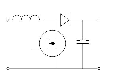
Flyback converters. The step-down converters produce output voltages less than
the input voltage. However, a change in the chopper configuration provides higher load volt-
ages. In step-up flyback converter (Fig. 4.11), the inductor L is placed directly between the
input source U
in
and the switch T. The anode lead of the rectifier D is placed on the node
where the switch and inductor are connected, and the capacitor C is placed between the
rectifier output and ground.
Fig. 4.11
The flyback operation can be broken into two periods. When the power switch is on, current
is being drawn through the inductor, which causes energy to be stored within its coil mate-
rial. The inductor current increases almost linearly. The switch then turns off. Since the cur-
rent through the inductor cannot change instantaneously and is forced to flow through the
diode and the load, the inductor’s voltage reverses (flies back). This causes the rectifier to
turn on, thus dumping the inductor’s energy into the capacitor. The inductor current de-
creases. This process passes until the energy of inductor is emptied. Since the inductor
voltage flies back above the input voltage, the voltage of the capacitor becomes higher than
the input voltage. When the capacitor voltage reaches the desired level, the switch turns on
ones more. The capacitor cannot discharge via the switch, as diode is reverse biased. In this
way, a stable voltage typically twice the U
in
or more can be obtained. So far as
U
out
= U
in⋅
(t
on
+ t
off
) / t
off
= U
in
/ (1 – q),
for a variation of q in the range 0 < q < 1, the output voltage will vary in the range
U
in
< U
out
< ∞. This circuit is particularly useful when operating on low-voltage supplies and
can lead to very cost-effective converter designs.
The transformer-isolated flyback converter shown in Fig. 4.12, a passes the energy when
the switch is off. The flyback circuit is similar to the forward transformer-isolated converter
but its secondary winding is reverse connected. During the first phase, the switch is on, the
+
–
D
T
L
C
U
out
U
in
