Ramanathan Sh. (Ed.) Thin Film Metal-Oxides: Fundamentals and Applications in Electronics and Energy
Подождите немного. Документ загружается.

4 Bipolar Resistive Switching in Oxides for Memory Applications 139
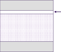
Fig. 4.7 Schematic
cross-section of the memory
element [20]
Top electrode Pt
Conductive
metal oxide
Bottom electrode Pt
Tunnel oxide
2-3nm
between 380 and 450
ı
C and result in a fully crystallized conductive metal oxide
and tunnel barrier. Quasi-static I–V curves of these stacks between ˙2 V are essen-
tially symmetric and the observed current scales with the tunnel oxide thickness.
Asymmetric behavior is observed at bias voltages higher than C2 V to the top elec-
trode and a regime of negative differential current indicates the programming of the
device into an OFF state. The operation is bipolar, i.e., a reversed voltage is needed
to erase this state. Applying voltage pulses of ˙3 V for pulse times between 1sto
10 s result in a change of the resistance of about 10. Cycling endurance is given
as 10
6
cycles.
Oxygen ion transport between the conductive metal oxide and the tunnel barrier
was proposed as the key step in the operation of the memory device structure. Based
on the ion migration model on an atomic scale for high electric fields an exponential
relation between the drift velocity of an ion in a dielectric material and the electric
field is found [20]. Due to the very high electric fields in the range of 10 MV/cm
(3 V/3 nm tunnel oxide thickness) the oxygen ions are mobile enough even at room
temperature to travel for a few nanometers. Under positive bias at the top electrode
oxygen ions migrate from the conductive metal oxide to the tunnel oxide and get
trapped. The excess negative charge accumulates in the tunnel oxide leading to a
decrease in the tunneling current through the tunnel oxide. The conductive metal
oxide ABO
3
compensates this charge loss by a metal cation valence change in the
cationic sublattice, which is a reduction process:
A
2C
B
4C
O
2
3
! A
2C
B
4C
1x
B
3C
x
O
2
30:5x
C 0:5xO
2
:
Figure 4.8 illustrates the write (RESET) operation.
Upon bias reversal the oxygen ions are transferred back to the conductive
metal oxide and the tunnel barrier recovers and the memory element switches
back to the ON state (SET or erase process). In [20] materials have not been dis-
closed. However, suitable candidate materials for the conductive metal oxide include
Pr
x
Ca
1x
MnO
3
(PCMO) in which the Mn
4C
=Mn
3C
valence change can compen-
sate for change in oxygen stoichiometry. With respect to the tunnel oxide not many
materials can withstand electric fields in the order of 10 MV/cm for prolonged pe-
riods of time [21]. Based on the published results on Time-Dependent Dielectric
Breakdown (TDDB) investigations for gate oxides Al
2
O
3
is a possible candidate
for the tunnel oxide material as theoretical dielectric breakdown fields of 11.2–
13.8 MV/cm have been reported [21].
140 R. Bruchhaus and R. Waser
Fig. 4.8 Schematic
representation of the write
(RESET) process. Oxygen
ions migrate under a high
electric field from the
conductive metal oxide into
the tunnel oxide. A valence
change in the cationic
sublattice compensates the
charge loss by the migrated
oxygen ions [20]
Top electrode Pt
Conductive
metal oxide
Bottom electrode Pt
Tunnel
oxide
+
−
2-
2-
2-
2-
2-
2-
E
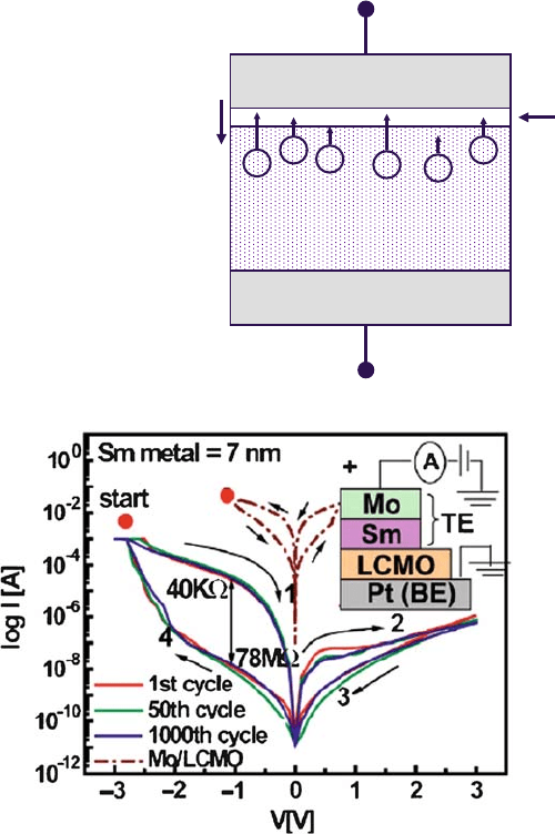
Fig. 4.9 I–V curves of the switching effects in the Mo/Sm/La
0:7
Ca
0:3
MnO
3
/Pt and
Mo/La
0:7
Ca
0:3
MnO
3
/Pt heterostructure [22]
4.3.2 Distributed Bipolar Switching in Complex Perovskites
A true interface-related switching effect is also claimed for the system Mo=Sm=
La
0:7
Ca
0:3
MnO
3
=Pt [22]. Figure 4.9 gives the layer sequence and the I–V
characteristics.
4 Bipolar Resistive Switching in Oxides for Memory Applications 141
Insertion of a thin Sm metal film between the complex oxide and the Mo top
electrode yielded a considerable decrease of the current levels and a significant im-
provement of the R
off
=R
on
ratio. Initially the layer stack is in the ON state. The
RESET process to the OFF state is observed during positive bias to the top Mo elec-
trode. At negative bias the sample switches back to the ON state. A R
off
=R
on
ratio
of 78 M=40 k D 1;950 was observed. An endurance of 1,000 switching cycles
was experimentally verified. The switching mechanism proposed in the paper is also
related to oxygen ion migration. Under positive bias to the top Mo electrode oxygen
ions migrate from the La
0:7
Ca
0:3
MnO
3
(LCMO) to the Sm metal film and form a
thin oxide film at the interface. The thin oxide film forms an isolating layer thus
preventing the flow of the electrical current. On negative bias the process is reversed
and the thin oxide layer removed and the ON state recovered. However, no proof is
given in the paper for the formation of the thin Sm oxide, which is claimed to be
responsible for the bistable switching.
More examples of interface type resistive switching in transition metal oxides
have been described in a recent review paper by Sawa [16]. To our knowledge,
Baikalov et al. [23] were the first who proposed that the resistance switching is
related to the metal/oxide interface in their Pr
0:7
Ca
0:3
MnO
3
samples with Ag elec-
trode. Based on the slow dynamics and the fact that the process can be accelerated
by higher voltages it was speculated that electrochemical processes like oxygen va-
cancy creation and/or migration may be involved [23]. However, no experimental
evidence was given in the paper.
In general, the memory elements described for RRAM have a capacitor-like MIM
structure in which an isolating wide bandgap semiconductor is sandwiched between
metal electrodes. Schottky barriers are expected to form at the interface between the
metal and the semiconductor due to the difference in workfunction. Sawa et al. [24]
investigated the p-type semiconductor Pr
0:7
Ca
0:3
MnO
3
(PCMO) in contact with dif-
ferent metal electrodes like SrRuO
3
(SRO), Pt, Au, Ag, and Ti. Among these, only
the sample Ti=PCMO=SRO=.100/SrTiO
3
-substrate with Ti electrode showed recti-
fying I–V characteristics and resistance switching. Nb-doped SrTiO
3
(Nb:STO) was
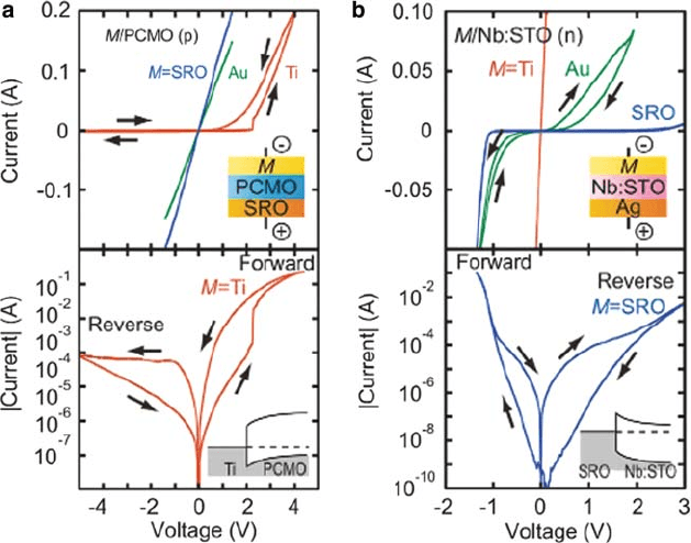
chosen as an example for a n-type semiconductor [25]. The results are summarized
in Fig. 4.10.
For the p-type PCMO the rectifying I–V characteristics is observed for the metal
(Ti) with the lowest work function of about 4.3 eV. On the other hand, the n-type
Nb:STO is rectifying for the SRO (and Au) electrode and resistance switching is
demonstrated for the SRO electrode. An additional series of experiments were per-
formed to further narrow down the interface width. Ti=Sm
0:7
Ca
0:3
MnO
3
(n unit
cells: u.c.)=La
0:7
Sr
0:3
MnO
3
[Ti/SCMO(n)/LSMO] films were deposited on (100)
SrTiO
3
single crystals with a 80-nm thick SRO bottom electrode. The SCMO is
insulating due to a narrow effective one-electron bandwidth, whereas the LSMO is
metallic due to a wide one-electron bandwidth [26, 27]. The 20-nm Ti top electrode
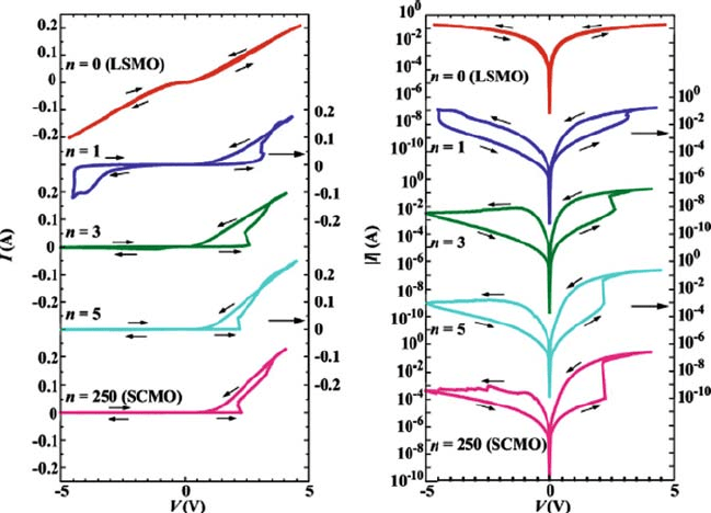
was deposited ex situ and protected by additional 380 nm of Au [28]. Fig. 4.11 gives
the I–V characteristics of the sample series with increasing number of unit cells n
from the top to the bottom. In the left panel the current is drawn in a linear scale,
the right panel gives the same curve with logarithmic scale.
142 R. Bruchhaus and R. Waser
Fig. 4.10 (a) I–V characteristics of M/p-type PCMO/SRO samples with M D Ti, Au, and SRO.
Only the sample with Ti electrode has a rectifying I–V curve and exhibits bipolar resistance switch-
ing. (b) I–V characteristics of M/n-type Nb:STO/Ag samples with M D Ti,Au,andSRO.The
samples with SRO (and Au) have a rectifying I–V characteristics. Bipolar resistance switching is
shown for the sample with SRO electrode. The insets in the upper part give the layer sequence and
in the lower part a sketch of the Schottky barrier at zero bias is given [16]
The pure Ti/LSMO .n D 0/ shows a slightly nonlinear but symmetric behavior.
Inserting a thin SCMO layer .n D 1/ results in a rectifying behavior similar to that
described in the earlier paper [24]. Together with the rectifying behavior a resistance
switching effect is observed, which becomes more obvious in the semilogarithmic
representation on the right side of Fig. 4.11. With increasing SCMO layer thickness
(n D 3, 5, and 250) both the rectifying as well as the switching behavior improve.
During positive bias (forward direction) the device switches from the OFF state to
the ON state. In the reverse direction (negative bias) the switching from the ON state
to the OFF state is observed. For the sample with n D 5 aR
off
=R
on
ratio of 6 10
2
is observed. The resistance switching can also be induced by voltage pulses. Fast
voltage pulses of 100 ns lead to small R
off
=R
on
ratios, ratios of more than 10 are
measured with a pulse length of 100 s for the sample stack with n D 5 [28].
Rectification and resistance switching was also observed in a series of samples
with SrTiO
3
single crystals n-doped with different levels of Nb of 0.002, 0.1, 0.2,
1 and 2%. [29]. SRO was used as the high workfunction metal electrode. The rec-
tifying characteristics is in agreement with that of a conventional n-type Schottky
diode. A clear resistance switching behavior was found for the 0.1, 0.2, and the
4 Bipolar Resistive Switching in Oxides for Memory Applications 143
Fig. 4.11 I–V characteristics of Ti/SCMO(n)/LSMO samples with n D 0,1,3,5,250drawnwith
a linear I scale (left) and a logarithmic I scale (right)[28]
1% Nb doping level in the forward bias direction. The sample with the smallest Nb
concentration shows some minor switching effect and no switching is observed for
the sample with 2% Nb. The resistance is switched from the ON state to the OFF
state under reverse (positive) bias stress. The SET process from the OFF state to the
ON state is observed under forward (negative) bias stress.
However, the proof of a Schottky barrier at the interface between properly
selected metals and semiconducting oxides alone does not explain the resistance
switching effect. For this some asymmetric modulation of the Schottky barrier as
a response to the applied voltage is needed. As a possible model for the switch-
ing effect, a charging effect of the Schottky-like interface is proposed [24, 25, 29].
Charging and discharging of trapping sites may modify the electronic properties of
the junction. This model is further supported by the finding that proper interface
engineering by doping can suppress the resistance switching effect. Insertion of a
2-nm thick undoped SrTiO
3
layer suppresses the switching by blocking the tun-
neling path but leaves the rectifying I–V characteristic unchanged. Heavy electron
doping by the insertion of 2 nm La
0:25
Sr
0:75
TiO
3
leads to a quasi Ohmic behavior
without switching and rectification [29]. The substitution of La
3C
for Sr
2C
provides
electrons into the conduction band. Now the SRO/La:STO/Nb:STO can be regarded
as a metal/n
C
/n-junction reducing the Schottky barrier width. Electrons possibly
can pass through the barrier by direct tunneling. These findings are summarized in
Fig. 4.12.
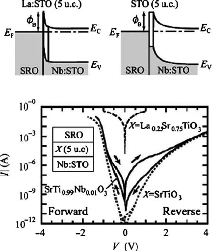
144 R. Bruchhaus and R. Waser
Fig. 4.12 Interface engineering of SrRuO
3
/X (2 nm)/SrTi
1x
Nb
x
O
3
.x D 0:01/ samples. Inser-
tion of the highly doped La
0:25
Sr
0:75
TiO
3
layer suppresses rectification and switching. Insertion
of 2 nm undoped isolator SrTiO
3
supresses the switching but leaves the rectifying behavior un-
changed. The induced changes are schematically depicted in the band diagrams [29]
The possibility of electrochemical redox reactions and migration of oxygen ions
is ruled out due to experimental finding that the Ti/LSMO sample did not show
the resistance switching [28]. However, an oxygen vacancy diffusion mechanism
was proposed by Nian et al. [30]forPr
0:7
Ca
0:3
MnO
3
(PCMO) films grown on Pt
bottom electrodes on TiN=SiO
2
=Si substrates. The PCMO films were grown by rf
sputtering at 500
ı
C under either oxygen rich .Ar W O
2
D 2 W 1/ or oxygen deficient
(Ar only) conditions. The PCMO films were 400 nm thick and Ag was deposited
by sputtering as the top electrode material. Based on the finding that the resistiv-
ity of ReAMnO
3•
such as LaBaMnO
3
increases by several orders of magnitude
when the oxygen content is reduced by 5%[31] it is proposed that under positive
voltage pulses oxygen ions are moved into the vacancies located at the metal elec-
trode interface (switching from OFF to ON). With negative bias the oxygen ions are
moved toward the metal interface and piling up there leaving a region with increased
oxygen vacancies which defines the OFF state. The local overdrive at the electrode
interface leads to a local nonequilibrium distribution which explains the resistance
decay observed in the I–V characteristic. The observation that an oxygen-annealing
step improved the resistance switching in metal-La
0:7
Ca
0:3
MnO
3
-metal heterostruc-
tures [32] supports the model that oxygen vacancies may play a key role in the
4 Bipolar Resistive Switching in Oxides for Memory Applications 145
resistance switching mechanism in oxides. For the bipolar switching effects based
on formation and rupture of filaments, discussed later in this chapter, the distinct
role of oxygen vacancies has been demonstrated.
Resistive switching, which is attributed to the interface, was also observed for
SrTiO
3
films deposited on SrTiO
3
substrates doped with 0.7% Nb [33]. In this
work, notable structural distortions were detected at the SrTiO
3
/0.7% Nb W SrTiO
3
interface by HRTEM. The switching process is interpreted as a trapping–detrapping
process of carriers in the interfacial region. This is concluded by comparison with
samples deposited on 0.1% Nb-doped SrTiO
3
substrates which did not switch and
had a well-matched interface structure with sharp contrast [33]. An interface-related
switching was also reported for La
1x
Sr
1Cx
MnO
4
single crystals with Ti electrode
[34]. Bistable switching was observed in Pr
1x
Ca
x
MnO
3
.x D 0:3/ (PCMO) thin
films at room temperature [35]. These films were grown in a polycrystalline state on
the highly (111) oriented Pt electrode. Evaporated Ag was used as the top electrode
material. The sample exhibited bipolar switching with a R
off
=R
on
ratio between 10
and 100. The switching voltage was less than 2 V for the 150-nm thick films. The
I–V characteristics was characterized in the frame of a trap-controlled space-charge
limited current (SCLC) mechanism [35].
4.4 Localized Bipolar Switching Effects in Transition
Metal Oxides
4.4.1 Filamentary Switching in Cr-Doped SrTiO
3
Single Crystals
Clear evidence for a localized conducting filament-based bipolar switching behavior
in transition metal oxides was obtained on single-crystal samples [36]. 0.2mol%
Cr-doped SrTiO
3
single crystals with Pt electrodes deposited on the surface with
a separation of 50 m were exposed to an electric field of 10
5
V=cm for 30 min
(“conditioning process”). The initially isolating crystal becomes conducting and can
be switched between an ON state and an OFF state by application of bipolar bias
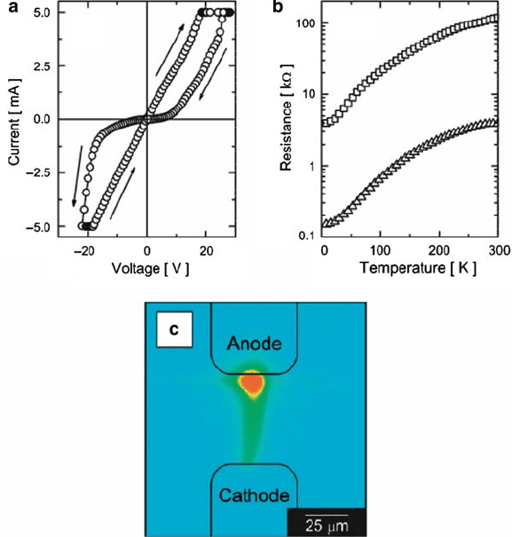
voltages, Fig. 4.13.
Negative bias voltages switch the sample from the OFF state to the ON state and
the opposite polarity triggers the RESET process. The finding that both the ON state
and the OFF state indicate a metallic behavior in the resistance versus temperature
plot of Fig. 4.13b are in contrast to models that describe the resistance switch-
ing as an alteration of a Schottky barrier [24] or nonpercolative metallic domains
[37]. For both models a nonmetallic temperature dependence is expected. Detailed
information about the microscopic nature of the conducting path were received
by micro-X-ray fluorescence (XRF) and X-ray absorption near edge spectroscopy
(XANES) at the Cr and Ti absorption K-edges. Based on these measurements it was
concluded that the conditioning process forms a few micrometer wide path of oxy-
gen vacancies between the electrodes. The Cr ions in the lattice serve as a kind of
146 R. Bruchhaus and R. Waser
Fig. 4.13 (a) Bipolar resistance switching between the OFF state and the ON state after “con-
ditioning.” (b) Temperature dependence of the resistance for the ON state and the OFF state
indicating metallic behavior for both states. (c) IR thermal image of the memory cell with a cur-
rent of 5 mA showing an area of increased temperature in front of the anode and a filament like
conduction profile between the anode and the cathode [36]
seed because the oxygen vacancies are preferentially associated with the Cr ions and
arranged along the conducting path like pearls in a pearl necklace. The Ti cations
compensate for the oxygen deficiency by reduction to Ti
.4n/C
species which is
equal to filling the Ti 3d band and leads to a metallic conduction [38]. The switch-
ing process itself is localized in the vicinity of the anode. Close to the anode is an
area of higher resistance as indicated by the higher temperature in the thermal mi-
croscopy. It is proposed that under negative bias pulses positively charged oxygen
vacancies migrate preferentially into this high-resistance interface region leading to
the ON state. Under positive bias the oxygen vacancies are repelled from the anode
region and the OFF state is recovered.
4 Bipolar Resistive Switching in Oxides for Memory Applications 147
4.4.2 Filament Fine Structure Analysis with Conductive-Tip AFM
Undoped SrTiO
3
single crystals were used for conductive-tip atomic force
microscope (C-AFM) investigations of the filament fine structure [39]. SrTiO
3
is a well-suited material for this purpose as it has a simple cubic structure, it is
a model band insulator and widely investigated for many years. In addition, high
quality single crystals are easily available. C-AFM turned out to be an invaluable
tool in a twofold sense. First it allows one to examine very small features with a
sufficient spatial resolution and, secondly, the tip can be used as nano-sized elec-
trode to locally apply bias voltages and study the local conductivity at the same
time. Dislocations and the preferred oxygen transport along these defects play the
key role to explain the bistable switching observed in this material. A three step
process was developed to activate the highly isolating single crystals and transform
them into a stable resistance switching material [39]. The treatment starts with an
annealing under reducing conditions then a holding time under ambient conditions
and, finally, application of an electric field under ultrahigh vacuum [40–42]. After
this sequence of treatments the sample material is in a metallic state and exhibits
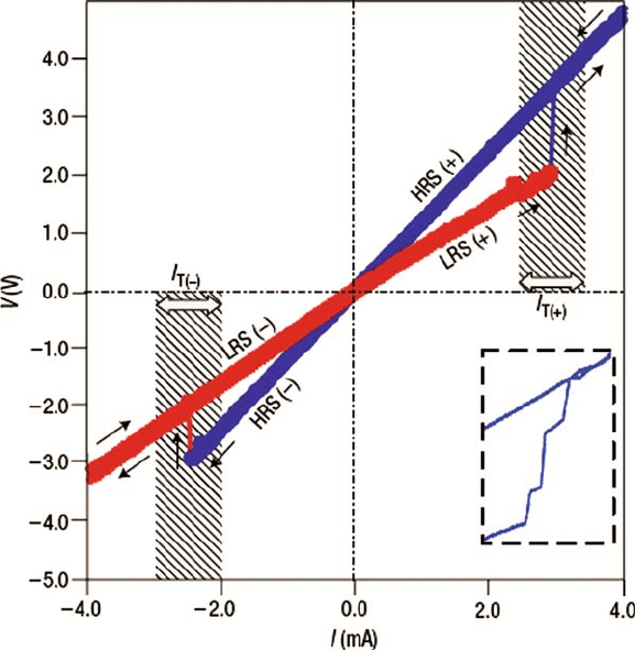
bistable switching under application of a bias current, Fig. 4.14.
Both, the OFF state and the ON state exhibit a metallic resistance versus tem-
perature behavior which is indicated by a positive temperature coefficient. The
filamentary type of conduction can already be observed in the optical microscope.
Inspection using an optical microscope reveals streaks formed between the cath-
ode and the anode in various segments. The streaks are arranged orthogonal along
the f100g direction of the crystal. At spots where a streak happened to cross the
surface an increased conductivity was observed by C-AFM. By observation under
higher magnification close to the anode gas bubbles lift the anode metallization
which result by electrochemical oxidation of the oxygen ions to form gaseous
O
2
.[39]
The C-AFM is an excellent tool to map spatial variation of electrical conductance
at the sample surface. Using step one and two of the preparation method described
above conducting spots could be observed by C-AFM, Fig. 4.15.
The spots are typically 2–4nm in diameter and the density is around 10
11
cm
2
.
With the C-AFM the electroformation process could be initiated at the surface.
A negative voltage applied to the tip resulted in a considerable increase in con-
ductivity over several orders of magnitude. These spots can be repeatably switched
between the OFF state and the ON state by application of appropriate bipolar bias
voltages. A range of at least 3 orders of magnitude was observed after reading the
states with a read voltage of 0.1 V well below the switching voltage. Direct evidence
that these conducting spots are related to the dislocations were received on samples
which have been subjected to a chemical etch treatment before the forming heat
treatment described above. The chemical etching makes the dislocations visible as
etch pits and the conducting spots are found within the center of these etch pits. The
studies performed on undoped single crystalline SrTiO
3
revealed the key role of de-
fects in the form of dislocations and their role as preferential path for the transport of
oxygen to serve as a model to explain the filamentary bistable resistance switching.
148 R. Bruchhaus and R. Waser
Fig. 4.14 V–I curves taken under current control mode to avoid damage to the samples and the
C-AFM tip. Bistable switching between the OFF state and the ON state is observed within a crit-
ical current window. The inset gives an example for a multistep transition which is occasionally
observed [39]
4.4.3 Filament Fine Structure Analysis on Thin Film Samples
However, for the use of resistive memory elements in a high-density RRAM with
feature size in the sub 100 nm range the active oxide layer in the MIM structure
must be fabricated as a thin film. Results received on single crystals are very useful
for the basic understanding of the switching mechanisms and due to high quality of
the crystal the impact of side-effects like grain-boundaries,internal stresses from the
deposition process, integration damage and pronounced impact from the interface
between oxide and electrode are suppressed. Fortunately, SrTiO
3
can be deposited
in high-quality on lattice matched substrates and electrodes. Results received on
these high-quality epitaxially grown thin films can be compared with the results on
the single crystals and the impact of sample thickness studied and thereby the actual
depth in which the filamentary switching process occurs narrowed down. Pulsed
laser deposition was used to deposit 10-nm thick SrTiO
3
thin films on 100-nm thick
