Qiu X.G. (Ed.) High Temperature Superconductors
Подождите немного. Документ загружается.

152 High-temperature superconductors
1
2
3
4
5
6
7
8
9
10
1
2
3
4
5
6
7
8
9
20
1
2
3
4
5
6
7
8
9
30
1
2
3
4
5
6
7
8
9
40
1
2
43X
© Woodhead Publishing Limited, 2011
Since the HTS deposition takes place at 650–900 °C, the thermal expansion
coefficients of the substrates and the HTS films have to match, or else the different
contraction of HTS film and substrate on cooling to room or even cryogenic
temperature will lead to mechanical stress, which can only be tolerated by the film
up to a certain maximum thickness without crack formation.
51
Many research
results
52
have shown that the residual compressive stress may cause the film to
delaminate from the substrate. The residual tensile stress may result in microcracks
in the film, which perhaps is the reason for the drop in J
c
. Hence, it is important to
study residual stress in YBCO superconducting thin films, and also necessary to
clarify all the mechanisms which influence the critical current properties and
to find a method for estimating J
c
for the optimum design of superconducting
layer thickness in the case of each application.
This chapter has two main components. Section 4.4 introduces sputtering
technique with a modulated biaxial rotation mode and describes the epitaxial
growth of large area double-sided YBCO films. In section 4.5, the thickness
dependence of YBCO films is studied in the range of 0.2–2 µm. The influence of
thickness-induced residual stress on surface morphology and electrical properties
is also investigated.
4.2 Sputter deposition technique
Sputtering is the process of removing atoms from the surface of a target by kinetic
energy transferred from an incoming flux of highly energetic particles. This
technique, in particular geometries or with specific deposition parameters, is able
to stoichiometrically transfer the composition of the target to the growing film,
53,54
and this characteristic makes it highly suited to the growth of multi-element
compounds such as complex oxides, with relative ease, compared to thermal
processes such as evaporation and PLD.
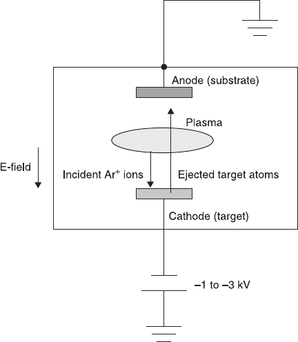
A schematic of the electrode configuration for basic sputtering process is shown in
Fig. 4.1. The source material or target is attached to the cathode. An electric field of
sufficient strength is applied between the anode and cathode, causing the ionization
of the gas between the electrodes. The gas is typically Ar, which is ionized to Ar
+
.
The Ar
+
ions are accelerated by the electric field towards the target, while electrons
are attracted to the anode. The heavy Ar
+
ions bombard the target, transferring their
kinetic energy to the target, and causing the atoms at or near the surface of the target
to be ejected. The ejected target atoms are then collected onto a heated substrate.
The synthesis of HTS thin films generally involves problems such as multi-
component control and negative-ion bombardment effect. In the case of oxide
targets, it is found that when the cathode is a planar disc and the substrates are
facing the cathode, the film composition deviates significantly from that of the
target, the film thickness is unexpectedly small and, even for very low sputtering
pressures, no film is deposited, although the substrate surface shows signs of
sputter etching. These effects are due to the bombardment of the substrates with
Sputter deposition of large-area double-sided YBCO films 153
1
2
3
4
5
6
7
8
9
10
1
2
3
4
5
6
7
8
9
20
1
2
3
4
5
6
7
8
9
30
1
2
3
4
5
6
7
8
9
40
1
2
43X
© Woodhead Publishing Limited, 2011
the negatively charged particles emerging from the cathode during deposition.
Such particles (e.g., O
–
, O~, BaO
–
) are generated at the surface of the cathode,
simply due to the fact that many of the sputtered species containing oxygen leave
the cathode surface in a negatively charged state due to their strong electronegativity.
The negatively charged species then are accelerated away from the cathode by the
voltage gap of the cathode dark space in the sputtering discharge. In other words,
the negative ions bombard the film surface with the same energy as the argon ions
bombard the target surface.
There are, in principle, two technical possibilities of reducing these
bombardment effects at the substrate position. The first possibility is to work with
the sputtering gas at very high pressure (e.g., 400–600 Pa) in order to thermalize
the fast particles before they reach the substrates. Unfortunately, this method will
result in a significant reduction of the sputtering rate. The second possibility,
which has been the most widely used since the discovery of the HTS, is to work
in the commonly used gas pressure region (10–20 Pa) and to avoid substrate
bombardment by proper choice of the position of the substrates. More strictly
speaking, the substrate position is optimum at locations where the ratio of
bombardment rate and deposition is minimized. For the planar magnetron, many
experimenters found these positions to be in the center of the plasma ring with the
4.1 Schematic diagram of a basic sputtering system. The target is
attached to the cathode, which is negatively biased compared to the
rest of the system.
154 High-temperature superconductors
1
2
3
4
5
6
7
8
9
10
1
2
3
4
5
6
7
8
9
20
1
2
3
4
5
6
7
8
9
30
1
2
3
4
5
6
7
8
9
40
1
2
43X
© Woodhead Publishing Limited, 2011
substrates facing the target plane. Another possibility is to place the substrates
outside of the plasma ring, at a suitable angle, in order to maximize the deposition
rate, which is known as ‘off-axis’ geometry. In order to improve the uniformity of
the film thickness distribution and deposition rate for off-axis geometry, it is
possible to sputter from two opposing planar targets. In this case, the negative
particles from one target sputter the opposite one and thus are easily neutralized
by stripping, and proceed as neutral particles which are no longer influenced by
electric or magnetic fields. This may serve to increase the deposition rate, at least
at very low pressures. To further increase deposition rate, many opposing targets
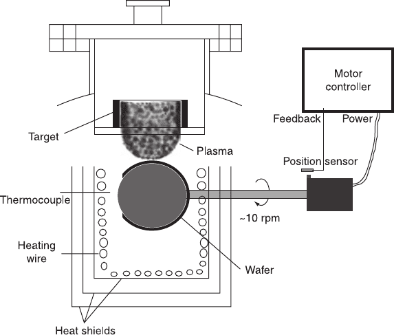
can be placed in a circle. The result is a tubelike target, called an ‘inverted
cylindrical target’, as shown in Fig. 4.2.
Therefore, a single inverted cylindrical (IC) sputter gun is employed in our
sputtering systems (shown schematically in Fig. 4.2) to simultaneously deposit
YBCO thin films on both sides of the substrate. The substrate rotates in an out-of-
plane mode in all of the deposition processes, which is driven by a speed adjustable
motor through a magnet-coupled feed through. The rotation speed is controlled by
the signal of position sensors. In fact, the biaxial rotation is also helpful in terms
of partially avoiding negative oxygen ion bombardment.
In the beginning, we always isolated the substrate from the targets with
shielding. In this way we could pre-sputter the YBCO target until it has a stable
4.2 Schematics of IC sputtering systems for simultaneous deposition
of large-area double-sided YBCO thin films.

Sputter deposition of large-area double-sided YBCO films 155
1
2
3
4
5
6
7
8
9
10
1
2
3
4
5
6
7
8
9
20
1
2
3
4
5
6
7
8
9
30
1
2
3
4
5
6
7
8
9
40
1
2
43X
© Woodhead Publishing Limited, 2011
voltage and current. After the substrate was loaded, the heater was set to a fixed
temperature. Then argon and oxygen were mixed and inlet into the chamber. The
gas flow rates were adjusted with mass flow controllers. After pre-sputtering, we
shifted the shielding away from the target and deposited for 36 hours with an
inverted cylindrical target to achieve a 500 nm thin film. The deposition parameters
are shown in Table 4.1. After the deposition, the sample was cooled down and
kept at 400 °C in 1 atm oxygen for 30 minutes in order to fully transform the non-
superconducting tetragonal phase into the superconducting orthogonal phase.
4.3 Epitaxial YBCO thin films
The growth of HTS thin films involves a specific optimization of the synthesis
process in order to achieve optimum superconducting properties. Since HTS
materials are multi-cation oxides with rather complex crystal structures, the
general requirements for the formation of HTS films with little or no impurity
phase include stringent control of the composition during the deposition process.
Even with the correct cation composition, the formation of a specific HTS oxide
phase requires an optimization of both the temperature and the oxygen partial
pressure, consistent with the phase stability.
The epitaxial growth and characterization of YBCO thin films has received
significantly more attention than any other HTS compound. Compared with other
HTS materials, epitaxial YBCO films are the easiest to synthesize and to achieve
a T
c
for the film that is near the bulk value. This is partly due to the relative
stability of the YBa
2
Cu
3
O
7
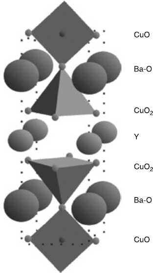
phase. The structure of YBa
2
Cu
3
O
7 –
δ
, shown
schematically in Fig. 4.3, can be derived by stacking three oxygen-deficient
perovskite unit cells (ACuO
y
) in the layered sequence, BaO–CuO
2
–YCuO
2
–
BaO–CuO. YBa
2
Cu
3
O
7
contains two CuO
2
planes per unit cell, separated by a Y
atom. CuO chains lie between the BaO layers. The oxygen content can be varied
from
δ
= 0 to
δ
= 1 through the removal of oxygen from the CuO chain layer.
Table 4.1 Deposition parameters for YBCO thin films
Sputtering power 100 W
Deposition rate 0.24 nm/min
Total pressure 45 Pa
O
2
:Ar 1:2
Substrate temperature 800 °C
Substrate ≤ 76 mm
Target–substrate distance 50 mm
Dimension of the cylindrical ∅50 mm × 40 mm
target (inner surface)
In-plane rotation speed 0.5 r/min
Average out-of-plane rotation speed 30 r/min
Modulation ratio 1–3
156 High-temperature superconductors
1
2
3
4
5
6
7
8
9
10
1
2
3
4
5
6
7
8
9
20
1
2
3
4
5
6
7
8
9
30
1
2
3
4
5
6
7
8
9
40
1
2
43X
© Woodhead Publishing Limited, 2011
Fully oxygenated YBa
2
Cu
3
O
7
is a hole-doped superconductor with T
c
= 92 K.
The crystal structure is orthorhombic with a = 3.82 Å, b = 3.88 Å, and
c = 11.68 Å.
55
When the oxygen content decreases, namely
δ
is from 0 to 1,
YBCO changes from an orthorhombic type to a tetragonal type with deteriorated
superconducting properties.
Epitaxial YBCO thin films were successfully grown on different single-crystal
substrates, such as LaAlO
3
, MgO, SrTiO
3
, and sapphire, with excellent crystal
perfection using our sputter system. J
c
of 2–4 MA/cm
2
at 77 K in self-filed and R
s
lower than 200
µΩ
for 10 GHz at 77 K is typical for high quality films. YBCO is
less anisotropic than other hole-doped HTS materials. These collective properties
make YBCO films quite attractive for many applications.
4.4 Issues related to scale-up
4.4.1 Large-area deposition
With simple out-of-plane rotation, uniform double-sided YBCO films could be
realized only on a very small area, usually less than one inch with a reasonable
4.3 Unit cell of YBa
2
Cu
3
O
7
.
Sputter deposition of large-area double-sided YBCO films 157
1
2
3
4
5
6
7
8
9
10
1
2
3
4
5
6
7
8
9
20
1
2
3
4
5
6
7
8
9
30
1
2
3
4
5
6
7
8
9
40
1
2
43X
© Woodhead Publishing Limited, 2011
substrate-to-target distance, D
s-t
. Or else, a larger uniform area must be traded with
a lower deposition rate with a longer D
s-t
or with an in-plane rotation or linear scan.
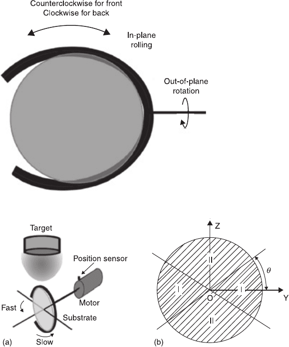
We designed a special biaxial rotation,
56
which combined the out-of-plane
rotation and an automatic interval in-plane rotation (rolling might be better, driven
by substrate weight) together, shown in Fig. 4.4. With this rotation, we could
produce uniform double-sided films on 2-inch wafer without extending D
s-t
(kept
at about 50 mm) so the deposition rate could be maintained. Taking into account
the clamp shadowing effect, uniform 3-inch films were also prepared with a
modulated biaxial rotation, in which the rotation speed was adjusted according to
different substrate postures in every out-of-plane revolution. The schematics of
speed-modulated biaxial rotation and the corresponding speed modulation regions
are shown in Fig. 4.5. When the substrate faces the target, we promote its speed
4.4 Special clamp design for in-plane wafer rotation.
4.5 (a) Schematic showing configuration with speed-modulated biaxial
rotation; (b) regions for out-of-plane speed modulation.
158 High-temperature superconductors
1
2
3
4
5
6
7
8
9
10
1
2
3
4
5
6
7
8
9
20
1
2
3
4
5
6
7
8
9
30
1
2
3
4
5
6
7
8
9
40
1
2
43X
© Woodhead Publishing Limited, 2011
and slow it down as its edge goes near to the target. By adjusting the speed ratio
in the two regions, shown in Fig. 4.5(b), we can modulate the lateral thickness
distribution and still keep the equality of both sides.
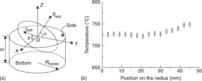
The film crystallization temperature is critical for high quality YBCO films,
especially for large-area deposition. Many groups have designed different heaters
for YBCO film growth. In our single-target system, a one-end-open tube-like heater
was made with rounded Thermocoax heating wire, the dimensions of which were
100 mm in diameter and 75 mm in height, as shown in Fig. 4.6(a). The substrate was
loaded near to the opening and facing the target. Its temperature distribution is
shown in Fig. 4.6(b). From the profile that can be seen in Fig. 4.6(b), we know that
the temperature is uniform in the radius direction, but changes considerably in the
axial direction – by more than 10 °C/mm. In fact, the plasma can compensate for the
heat loss caused by the heater opening. Within the region that the 3-inch wafer
passes through, the temperature deviation is about 20 °C when plasma is off, and is
reduced to 5 °C when the plasma is on. With a 10 to 60 rpm rotation, the substrate
temperature distribution must be more uniform because of the cyclic compensation
and the heat conduction inside the substrate itself.
4.4.2 Film homogeneity
In sputtering, there are three possible reasons for multicomponent oxide films not
to be homogeneous:
1 Different angular distribution of atom emission. The atoms will be emitted
from the target surface with determinate distribution for a given condition,
4.6 (a) Geometrical relation of substrate and cylindrical target for
biaxial rotation (X, Y, Z = three dimensional coordinates, H = heater
height, r
sub
= substrate radius, R
heater
= heater radius, n
sub
= substrate
normal,
α
= included angle between the substrate normal and
Y-coordinate, θ = included angle between substrate horizontal and
X-coordinate); (b) measured temperature distribution along the radius
of the upper opening of the cylindrical heater.
⨡
Sputter deposition of large-area double-sided YBCO films 159
1
2
3
4
5
6
7
8
9
10
1
2
3
4
5
6
7
8
9
20
1
2
3
4
5
6
7
8
9
30
1
2
3
4
5
6
7
8
9
40
1
2
43X
© Woodhead Publishing Limited, 2011
and become thermalized and transfer diffusively due to colliding with atoms
in a high pressure environment. Therefore, atoms with different masses have
different angular concentration distributions.
2 Negative ion bombardment originating from the cathode. Negative ions are
accelerated by the electrical field and can strike the substrate with high energy.
The bombardment will selectively re-sputter the film according to different
sputtering yields.
3 Possible difference of deposition parameters. For instance, if the deposition
temperature is not uniform across the entire substrate, different sticking
coefficients will result in inhomogeneity.
So, both the substrate-to-target distance (D
s-t
) and the angle (
θ
s-t
) are continuously
varying rather than fixed, as in an off-axis mode. Therefore, the negative ion
bombardment was also partially eliminated by the substrate tilting in the process.
In our experiment, we deposited large-area NdBa
2
Cu
3
O
7 –
δ
(NBCO) films on
aluminum sheets at room temperature (without the heater) for composition and
thickness distribution analysis.
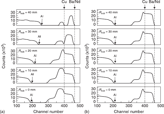
Figure 4.7(a) shows the RBS spectra of NBCO film deposited on a static
aluminum sheet for 5 hours with a 50 mm D
t-s
. From the peak intensities of Cu, it
is obvious that the central film is Cu-rich, and that the barium and neodymium
concentrations at the edge are much higher than those in the center. Because the
atom numbers of barium and neodymium are very close and difficult to distinguish,
4.7 RBS results along the radius of the samples: (a) sample with static
substrate; (b) sample with speed modulated bi-axial rotation.
160 High-temperature superconductors
1
2
3
4
5
6
7
8
9
10
1
2
3
4
5
6
7
8
9
20
1
2
3
4
5
6
7
8
9
30
1
2
3
4
5
6
7
8
9
40
1
2
43X
© Woodhead Publishing Limited, 2011
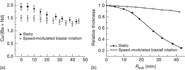
(Ba + Nd) was taken together for concentration distribution. Besides Cu and
(Ba + Nd) concentrations, the concentration ratio of Cu/(Ba + Nd) was taken as a
comparable parameter for the extent of stoichiometry. The ratio is equal to 1 for
stoichiometric NBCO film. The maximum difference, (max − min)/mean, of Cu
concentrations is 28%, the maximum difference of (Ba + Nd) concentrations is
21%, and the ratios of Cu/(Ba + Nd) range from 1.3 to 2.2 within ∅86 mm (solid
squares in Fig. 4.8(a)). The relative thickness distribution was determined by
RBS (solid squares in Fig. 4.8(b)) and is consistent with that measured by the
profiler. Further, we measured the aluminum peak shift for valuating the thickness
distribution – it was also valid. The maximum film thickness deviation from center
to edge is as much as 75% within ∅86 mm.
Biaxial rotation is designed specially for the simultaneous deposition of double-
sided large-area thin films. In this case, the substrate edge can go very near to the
target and catch more atoms in the high particle density region. With speed
modulation, the distribution could be further improved and uniform film thickness
could be obtained.
Figure 4.7(b) shows RBS spectra of film deposited with 60 mm target-to-
substrate distance for 10 hours in single-target system with speed modulated
biaxial rotation. Within ∅84 mm, the maximum difference of Cu concentrations
is only 6%, while the maximum difference of (Ba + Nd) concentrations is only
8%. The homogeneity of Cu concentration is much improved by biaxial rotation
(open circles, as shown in Fig. 4.8(a)). The thickness distribution of biaxial
rotation (open circles, shown in Fig. 4.8(b)) is much better than that of a static
substrate. Within the ∅80 mm range, the maximum thickness deviation is limited
to 10%.
With the speed modulation technique, high quality double-sided YBCO films
have been deposited on 3-inch LaA1O
3
substrates with very good side-to-side
uniformities and lateral homogeneities. The deposition of 500 nm films can be
finished in 36 hours with about 14 nm/h deposition rate for both sides.
4.8 Stoichiometric (a) and thickness (b) distribution for static sample
(solid squares) and speed modulated biaxial rotating sample (open
circles).
Sputter deposition of large-area double-sided YBCO films 161
1
2
3
4
5
6
7
8
9
10
1
2
3
4
5
6
7
8
9
20
1
2
3
4
5
6
7
8
9
30
1
2
3
4
5
6
7
8
9
40
1
2
43X
© Woodhead Publishing Limited, 2011
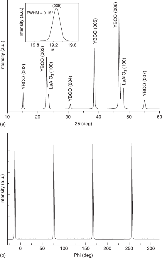
The samples were pure c-axis oriented and with good out-of-plane and in-plane
epitaxy, as shown in Fig. 4.9. The typical properties of a 3-inch sample are T
c
90 K,
∆T
c
about 0.5 K, J
c
2–4 MA/cm
2
, and R
s
less than 0.5
µΩ
. The T
c
, J
c
, and thickness
distributions are shown in Plate II in the colour section between pages 244 and 245.
4.9 (a) Typical XRD
θ
–2
θ
pattern of YBCO thin film on LAO substrates.
The inset is the corresponding rocking curve on YBCO (005) peaks; (b)
XRD ∅-scan of the same YBCO thin film.
