Power electronic handbook
Подождите немного. Документ загружается.

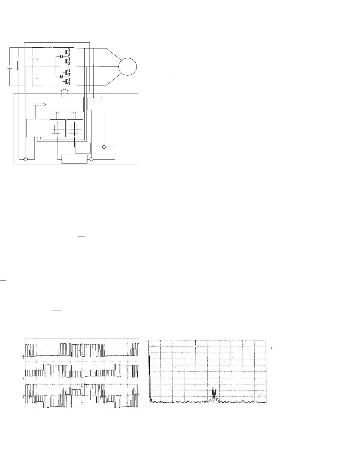
34 Control Methods for Switching Power Converters 977
−
−
v
o
+
−
+
+
+
+
+
+
+
−
i
o
d
(a) (b)
dt
i
2
i
1
i
r
i
+
dq
->
i d
r
i
q
r
Space
vector
decoder
&
driver
To power
switches
+
C
1
V
RMS
v
o
+
+
÷
÷÷
÷
R
αβ
α
β
12
->
αβ
ε
ρ
3
= 0
d
dt
+
+
-1
r
i d
max
LC
L-CRRc
α
β
1
2
3
4
5
6
0,7
v
o
r
β
×
×
×
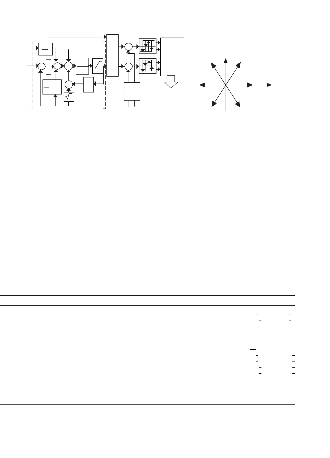
FIGURE 34.47 (a) Sliding-mode PWM controller modulator for the unity power factor three-phase PWM rectifier and (b) α, β space vector
representation of the PWM bridge rectifier leg voltages.
34.3.5.12 α, β Space Vector Current Modulator
Depending on the values of γ
k
, the bridge rectifier leg out-
put voltages can assume only eight possible distinct states
represented as voltage vectors in the α, β reference frame
(Fig. 34.47b), for sources with isolated neutral.
With only two independent currents, two three-level hys-
teresis comparators, for the current errors, must be used in
order to accurately select all eight available voltage vectors.
Each three-level comparator can be obtained by summing
the outputs of two comparators with two levels each. One
of these two comparators (δ
Lα
, δ
Lβ
) has a wide hysteresis
width and the other (δ
N α
, δ
N β
) has a narrower hystere-
sis width. The hysteresis bands are represented by ε and ρ.
Table 34.1 represents all possible output combinations of
the resulting four two-level comparators, their sums giving
TABLE 34.2 Two-level and three-level comparator results, showing corresponding vector choice, corresponding γ
k
and vector α, β component
voltages; vectors are mapped in Fig. 34.47b
δ
Lα
δ
N α
δ
Lβ
δ
N β
δ
α
δ
β
Vector γ
1
γ
2
γ
3
v
α
v
β
−0.5 −0.5 −0.5 −0.5 −1 −1 2 110v
o
/
√
6 v
o
/
√
2
0.5 −0.5 −0.5 −0.5 0 −1 2 110v
o
/
√
6 v
o
/
√
2
0.5 0.5 −0.5 −0.5 1 −1 3 010−v
o
/
√
6 v
o
/
√
2
−0.5 0.5 −0.5 −0.5 0 −1 3 010−v
o
/
√
6 v
o
/
√
2
−0.5 0.5 0.5 −0.5 0 0 0or7 0or1 0or1 0or1 0 0
0.5 0.5 0.5 −0.5 1 0 4 011−
√
2/3v
o
0
0.5 −0.5 0.5 −0.5 0 0 0or7 0or1 0or1 0or1 0 0
−0.5 −0.5 0.5 −0.5 −101 100
√
2/3v
o
0
−0.5 −0.5 0.5 0.5 −116 101v
o
/
√
6 −v
o
/
√
2
0.5 −0.5 0.5 0.5 0 1 6 101v
o
/
√
6 −v
o
/
√
2
0.5 0.5 0.5 0.5 1 1 5 001−v
o
/
√
6 −v
o
/
√
2
−0.5 0.5 0.5 0.5 0 1 5 001−v
o
/
√
6 −v
o
/
√
2
−0.5 0.5 −0.5 0.5 0 0 0or7 0or1 0or1 0or1 0 0
0.5 0.5 −0.5 0.5 1 0 4 011−
√
2/3v
o
0
0.5 −0.5 −0.5 0.5 0 0 0or7 0or1 0or1 0or1 0 0
−0.5 −0.5 −0.5 0.5 −101 100
√
2/3v
o
0
the two three-level comparators (δ
α
, δ
β
), plus the voltage
vector needed to accomplish the current tracking strategy
(i
α,β
r
−i
α,β
) = 0 (ensuring (i
α,β
r
−i
α,β
)×d(i
α,β
r
−i
α,β
)/dt < 0),
plus the γ
k
variables and the α, β voltage components.
From the analysis of the PWM boost rectifier it is concluded
that, if, for example, the voltage vector 2 is applied (γ
1
= 1,
γ
2
= 1, γ
3
= 0), in boost operation, the currents i
α
and i
β
will both decrease. Oppositely, if the voltage vector 5 (γ
1
= 0,
γ
2
= 0, γ
3
= 1) is applied, the currents i
α
and i
β
will both
increase. Therefore, vector 2 should be selected when both i
α
and i
β
currents are above their respective references, that is for
δ
α
=−1, δ
β
=−1, whereas vector 5 must be chosen when
both i
α
and i
β
currents are under their respective references,
or for δ
α
= 1, δ
β
= 1. Nearly all the outputs of Table 34.2 can
be filled using this kind of reasoning.
978 J. F. Silva and S. F. Pinto
The cases where δ
α
= 0, δ
β
=−1, the vector is selected
upon the value of the i
α
current error (if δ
Lα
> 0 and δ
N α
< 0
then vector 2, if δ
Lα
< 0 and δ
N α
> 0 then vector 3). When
δ
α
= 0, δ
β
= 1, if δ
Lα
> 0 and δ
N α
< 0 then vector 6, else
if δ
Lα
< 0 and δ
N α
> 0 then vector 5. The vectors 0 and 7
are selected in order to minimize the switching frequency (if
two of the three upper switches are on, then vector 7, oth-
erwise vector 0). The space-vector decoder can be stored in a
lookup table (or in an EPROM) whose inputs are the four two-
level comparator outputs and the logic result of the operations
needed to select between vectors 0 and 7.
34.3.5.13 PI Output Voltage Control of the
Current-mode PWM Rectifier
Using the α, β current-mode hysteresis modulators to enforce
the i
d
and i
q
currents to follow their reference values, i
d
r
, i
qr
(the values of L and C are such that the i
d
and i
q
currents
usually exhibit a very fast dynamics compared to the slow
dynamics of v
o
), a first-order model (34.146) of the rectifier
output voltage can be obtained from Eq. (34.73).
dv
o
dt
=
1
C
−
RR
c
L
γ
d
i
d
r
+γ
q
i
q
r
−
R
c
γ
2
d
+γ
2
q
L
v
o
+
R
c
L
γ
d
v
d
+γ
q
v
q
−
i
o
C
−R
c
di
o
dt
(34.146)
Assuming now a pure resistor load R
1
= v
o
/i
o
, and a mean
delay T
d
between the i
d
current and the reference i
d
r
, con-
tinuous transfer functions result for the i
d
current (i
d
=
i
dr
(1+sT
d
)
−1
) and for the v
o
voltage (v
o
= k
A
i
d
/(1+sk
B
) with
k
A
and k
B
obtained from Eq. (34.146)). Therefore, using the
same approach as Examples 34.6, 34.8, and 34.11, a linear PI
regulator, with gains K
p
and K
i
(34.147), sampling the error
between the output voltage reference v
o
r
and the output v
o
,
0 0.01 0.02 0.03 0.04 0.05
−50
−40
−30
−20
−10
0
10
20
30
40
50
t [s]
i[A]
CH1 = 2V
CH1 = 2V
CH1 = 2V CH3 = 1V CH4 = 1V
5MS / d
06-JUL-1998
10 02
Stopped
DC DC DC DC
1
2
3
4
P10P10P10
P10
(a) (b)
FIGURE 34.48 α, β space vector current modulator operation at near unity power factor: (a) simulation result (i
1r
+30; i
2
r
+30; 2×i
1
;2×i
2
−30)
and (b) experimental result (1→i
1r
,2→i
2r
(10 A/div); 3→i
1
,4→i
2
(5 A/div)).
can be designed to provide a voltage proportional (k
I
)tothe
reference current i
d
r
(i
d
r
= (K
p
+K
i
/s)k
I
(v
o
r
−v
o
)).
K
p
=
R
1
+R
c
4ζ
2
T
d
R
1
K
1
γ
d
(1/C −RR
c
/L)
K
i
=
R
c
(γ
2
d
+γ
2
q
)/L
+
(
1/R
1
C
)
4ζ
2
T
d
K
1
γ
d
(1/C −RR
c
/L)
(34.147)
These PI regulator parameters depend on the load resistance
R
1
, on the rectifier parameters (C, R
c
, L, R), on the rectifier
operating point γ
d
, on the mean delay time T
d
, and on the
required damping factor ζ. Therefore, the expected response
can only be obtained with the nominal load and input voltages,
the line current dynamics depending on the K
p
and K
i
gains.
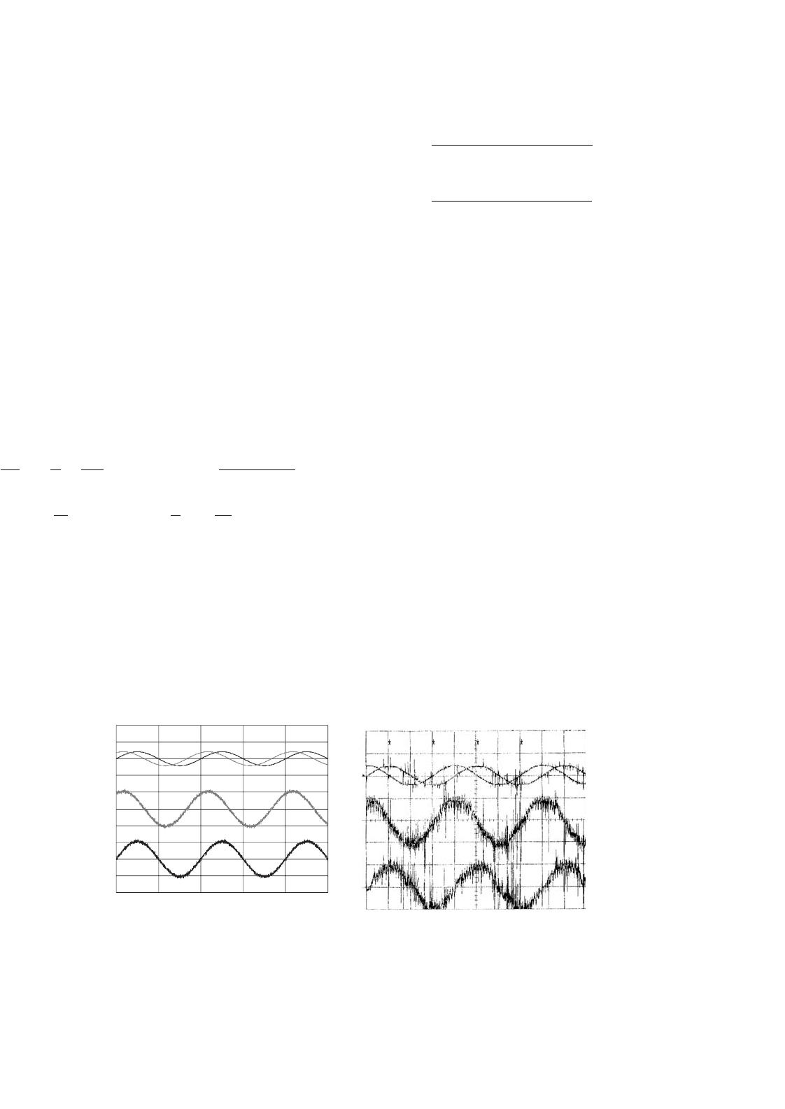
Results (Fig. 34.48) obtained with the values V
RMS
≈ 70 V,
L ≈ 1.1 mH, R ≈ 0.1 , C ≈ 2000 µF with equivalent series
resistance ESR≈ 0.1 (R
c
≈ 0.1 ), R
1
≈ 25 , R
2
≈ 12 ,
β = 0.0012, K
p
= 1.2, K
i
= 100, k
I
= 1, show that the α, β
space vector current modulator ensures the current tracking
needed (Fig. 34.48) [17]. The v
o
step response reveals a faster
sliding-mode controller and the correct design of the current
mode/PI controller parameters. The robustness property of the
sliding-mode controlled output v
o
, compared to the current
mode/PI, is shown in Fig. 34.49.
E
XAMPLE 34.15 Sliding-mode controllers for multi-
level inverters
Diode clamped multilevel inverters (Fig. 34.50) are the
converters of choice for high-voltage high-power dc/ac
or ac/ac (with dc link) applications, as the active semi-
conductors (usually gate turn-off thyristors (GTO) or
IGBT transistors) of n-level power conversion systems,
must withstand only a fraction (normally U
cc
/(n − 1))
of the total supply voltage U
cc
. Moreover, the out-
put voltage of multilevel converters, being staircase-like
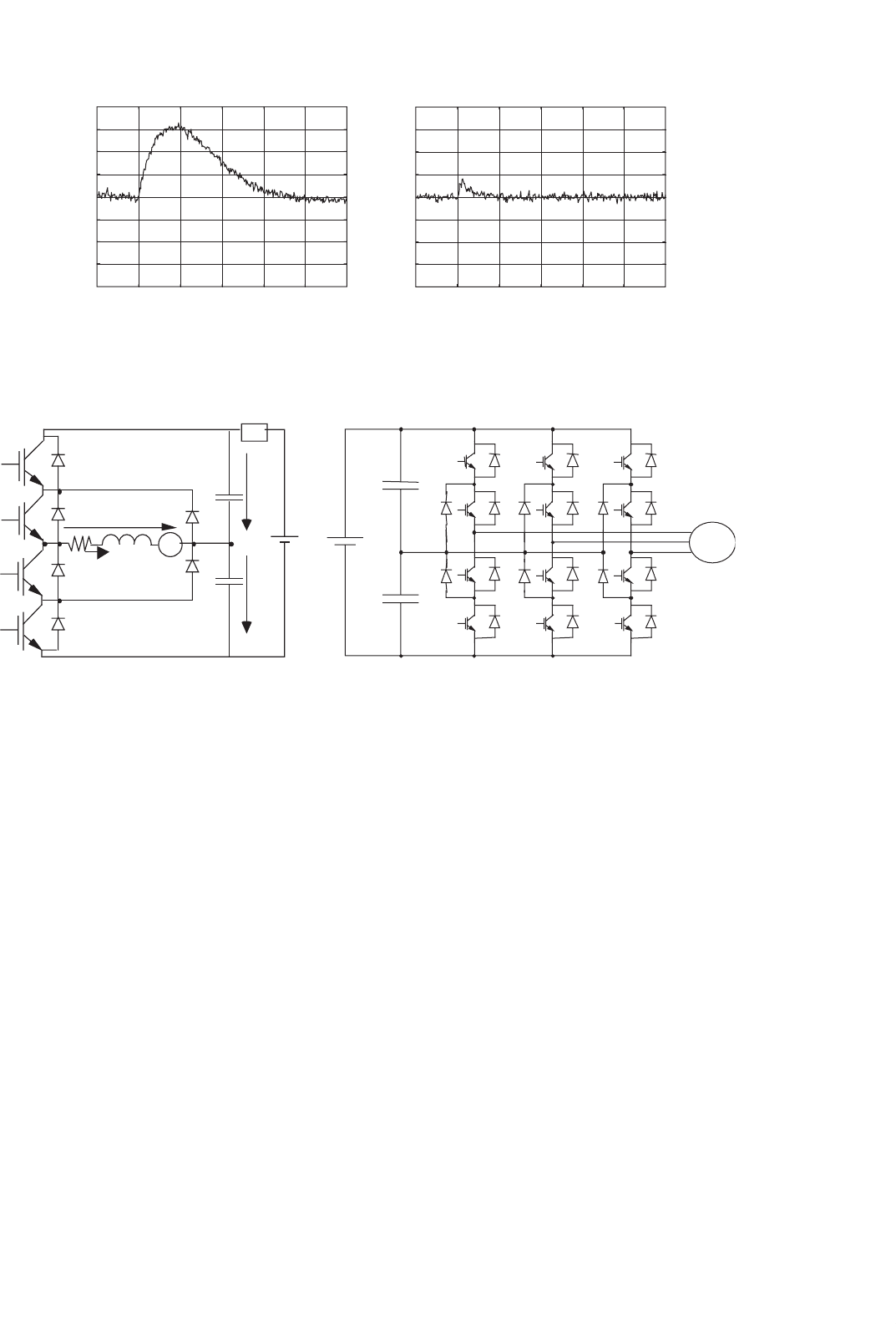
34 Control Methods for Switching Power Converters 979
–20
–15
–10
–5
0
5
10
15
20
0 0.005 0.01 0.015 0.02 0.025 0.03
v
c
–v
cref
[V]
t [s]
–20
–15
–10
–5
0
5
10
15
20
0 0.005 0.01 0.015 0.02 0.025 0.03
v
c
–v
cref
[V]
t [s]
(a) (b)
FIGURE 34.49 Transition from rectifier to inverter operation (i
o
from 8 to −8 A) obtained by switching off IGBT S
a
(Fig. 34.46) and using
I
a
= 16 A: (a) v
o
−v
or
[v] with sliding-mode control and (b) v
o
−v
or
[v] with current-mode /PI control.
S
1
C
1
V
E
U
cc
C
1
C
2
S
14
S
13
S
12
S
11
S
21
S
22
S
23
S
24
S
34
S
33
S
32
S
31
D
5
D
6
C
2
u
C2
u
cc
u
C1
Z
cc
S
2
S
3
Load
u
o
S
4
R
i
L
L
(a) (b)
AC
Load
FIGURE 34.50 (a) Single-phase, neutral point clamped, three-level inverter with IGBTs and (b) three-phase, neutral-clamped, three-level inverter.
waveforms with n steps, features lower harmonic distor-
tion compared to the two-level waveforms with the same
switching frequency.
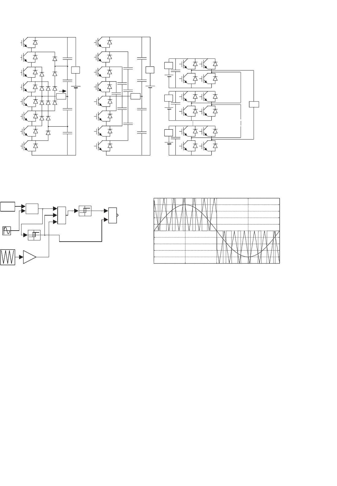
The advantages of multilevel converters are paid
into the price of the capacitor supply voltage dividers
(Fig. 34.51) and voltage equalization circuits, into the
cost of extra power supply arrangements (Fig. 34.51c),
and into increased control complexity. This example
shows how to extend the two-level switching law (34.97)
to n-level converters, and how to equalize the voltage of
the capacitive dividers.
Considering single-phase three-level inverters
(Fig. 34.50a), the open-loop control of the output
voltage can be made using three-level SWPWM. The
two-level modulator, seen in Example 34.9, can be
easily extended (Fig. 34.52a) to generate the γ
III
com-
mand (Fig. 34.52b) to three-level inverter legs, from the
two-level γ
II
signal, using the following relation:
γ
III
= γ
II
(m
i
sin(ωt) − sgn(m
i
sin(ωt))/2 − r(t)/2)
−1/2 +sgn(m
i
sin(ωt))/2 (34.148)
The required three-level SWPWM modulators for the
output voltage synthesis seldom take into account the
semiconductors and the capacitor voltage divider non-
ideal characteristics. Consequently, the capacitor voltage
divider tends to drift, one capacitor being overcharged,
the other discharged, and an asymmetry appears in the
currents of the power supply. A steady-state error in the
output voltage can also be present. Sliding-mode control
can provide the optimum switching timing between all
the converter levels, together with robustness to supply
voltage disturbances, semiconductor non-idealities, and
load parameters.
A. Sliding-mode switching law For a variable-structure sys-
tem where the control input u
i
(t) can present n levels, consider
the n values of the integer variable γ, being −(n − 1)/2 ≤
γ ≤ (n − 1)/2 and u
i
(t) = γU
cc
/(n − 1), dependent on the
topology and on the conducting semiconductors. To ensure
the sliding-mode manifold invariance condition (34.92) and
the reaching mode behavior, the switching strategy γ(t
k+1
)
980 J. F. Silva and S. F. Pinto
S1
S2
S3
S4
u
o
S5
S6
S7
S8
S1
S2
S3
S4
S5
S6
S7
S8
Cf
Cf
Cf
Cf
C1
C2
C3
C4
Cf
C4
C3
C2
C1
Zcc Zcc
Zcc
Zcc
Zcc
Ucc
Us
U2
U1
S1
S2
S1
S1
S2
S2
S3
S4
S3
S3
S4
S4
Load
Load
Load
(
a
)(
b
)(
c
)
FIGURE 34.51 (a) Five-level (n = 5) diode clamped inverter with IGBTs; (b) five-level (n = 5) flying capacitor converter; and (c) multilevel
converter based on cascaded full-bridge inverters.
+
+
+
−
−
×
Gama III
r(t) PU
Gama III
Sum4
Sine Wave
(PU)
Relay
Hysteresis 10
−5
High outut=0.5
Low output=-0.5
Product 2
0.8
Modulation
Index
0.5
Gain
0.5*sgn
0 0.005 0.01 0.015 0.02
−1
−0.8
−0.6
−0.4
−0.2
0
0.2
0.4
0.6
1
0.8
1
t[s]
Three-level PWM
(a) (b)
FIGURE 34.52 (a) Three-level SWPWM modulator schematic and (b) main three-level SWPWM signals.
for the time instant t
k+1
, considering the value of γ(t
k
)
must be
γ(t
k+1
) =
γ(t
k
) +1ifS(e
x
i
, t) >ε∧
˙
S(e
x
i
, t)
>ε∧ γ(t
k
) < (n −1)/2
γ(t
k
) −1ifS(e
x
i
, t) < −ε ∧
˙
S(e
x
i
, t)
< −ε ∧γ(t
k
) > −(n −1)/2
(34.149)
This switching law can be implemented as depicted in
Fig. 34.53.
34.3.5.14 Control of the Output Voltage in
Single-phase Multilevel Converters
To control the inverter output voltage, in closed-loop, in
diode-clamped multilevel inverters with n levels and supply
voltage U
cc
, a control law similar to Eq. (34.132), S(e
uo
, t) =
κ
u
o
r
−k
v
γ(t
k
)U
cc
/(n −1)
dt = 0, is suitable.
Figure 34.54a shows the waveforms of a five-level sliding-
mode controlled inverter, namely the input sinus voltage,
the generated output staircase wave, and the sliding-surface
instantaneous error. This error is always within a band cen-
tered around the zero value and presents zero mean value,
which is not the case of sigma-delta modulators followed by
n-level quantizers, where the error presents an offset mean
value in each half period.
Experimental multilevel converters always show capacitor
voltage unbalances (Fig. 34.54b) due to small differences
between semiconductor voltage drops and circuitry offsets.
To obtain capacitor voltage equalization, the voltage error
(v
c
2
−U
cc
/2) is fed back to the controller (Fig. 34.55a) to coun-
teract the circuitry offsets. Experimental results (Fig. 34.54c)
34 Control Methods for Switching Power Converters 981
+
+
s ±(n−1)/2
−eps;+eps
out:+1-1
Mux
Mux3
1
S(exi,t)
1
Gama
du/dt
dS/dt −eps;+eps
out:+1-1
Memory
f(u)
(u[1]*u[2]>0)*
*2-1
1
Gama
+
+
+
+
Decoder
−1.3eps;+1.3eps
out:-0.5,+0.5
−eps;+eps
out:-0.5,+0.5
−1.2eps;+1.2eps
out:-0.5,+0.5
−1.1eps;+1.1eps
out:-0.5,+0.5
1
S(exi,t)
(a)
(b)
FIGURE 34.53 (a) Multilevel sliding-mode PWM modulator with n-level hysteresis comparator with quantization interval ε and (b) four hysteresis
comparator implementation of a five-level switching law.
Voltage [V]
−1
0
1
0.02 0.025 0.03 0.035 0.04
Time [s]
u
o
vv
PWMPWM
r
S(e
xi
,t)
Voltage [V]
−20
−10
0
10
20
0.325 0.33 0.335 0.34 0.345
Time [s]
u
C1
v
PWMPWM
r
u
o
-u
C2
V
pwmrpwmr
u
o
Ucc/Ucc/2
(a) (b) (c)
v
PWM
r
u
C1
v
PWM
r
V
pwmr
u
o
Ucc/2
FIGURE 34.54 (a) Scaled waveforms of a five-level sliding-mode controlled single-phase converter, showing the input sinus voltage v
PWM
r
, the
generated output staircase wave u
o
and the value of the sliding surface S(e
x
i
,t); (b) scaled waveforms of a three-level neutral point clamped inverter
showing the capacitor voltage unbalance (shown as two near flat lines touching the tips of the PWM pulses); and (c) experimental results from a
laboratory prototype of a three-level single-phase power inverter with the capacitor voltage equalization described.
1/s
integral
3
kc*(uc2-Ucc/2)
2
kv vpwm
1
vpwmr
+
−
−
Sum4
1
Gama
n-level hysteresis
comparator
3
kc*(uc2-Ucc/2)
2
io
1
ior
1
Gama
n-level hysteresis
comparator
1/s
int
-K--K-
kp
+
−
−
Sum4
κ
FIGURE 34.55 (a) Multilevel sliding-mode output voltage controller and PWM modulator with capacitor voltage equalization and (b) sliding-mode
output current controller with capacitor voltage equalization.
clearly show the effectiveness of the correction made. The small
steady-state error, between the voltages of the two capacitors,
still present, could be eliminated using an integral regulator
(Fig. 34.55b).
Figure 34.56 confirms the robustness of the sliding-mode
controller to power supply disturbances.
34.3.5.15 Output Current Control in Single-phase
Multilevel Converters
Considering an inductive load with current i
L
, the control law
(34.107) and the switching law of (34.159), should be used
for single-phase multilevel inverters. Results obtained using
the capacitor voltage equalization principle just described are
shown in Fig. 34.57.
982 J. F. Silva and S. F. Pinto
−2
0
2
0 0.01
Voltage [V]
0.02 0.03 0.04 0.05
Time [s]
−2000
0
2000
0 0.01 0.02 0.03 0.04 0.05
Time [s]
Voltage [V]
−2
0
2
0 0.01 0.02 0.03 0.04 0.05
Time [s]
Voltage [V]
(a) (b) (c)
FIGURE 34.56 Simulated performance of a five-level power inverter, with a U
cc
voltage dip (from 2 to 1.5 kV). Response to a sinusoidal wave of
frequency 50 Hz: (a) v
PWM
r
input; (b) PWM output voltage u
o
; and (c) the integral of the error voltage, which is maintained close to zero.
−600
−400
−200
0
200
400
600
0 0.005 0.01 0.015 0.02 0.025 0.03 0.035 0.04 0.045 0.05
Time [s]
u
C1
i
Lr
i
L
u
o
−u
C2
FIGURE 34.57 Operation of a three-level neutral point clamped
inverter as a sinusoidal current source: Scaled waveforms of the out-
put current sine wave reference i
Lr
, the output current i
L
, showing ripple,
together with the PWM-generated voltage u
o
, with nearly equal pulse
heights, corresponding to the equalized dc capacitor voltages u
C
1
and u
C
2
.
EXAMPLE 34.16 Sliding-mode controllers for three-
phase multilevel inverters
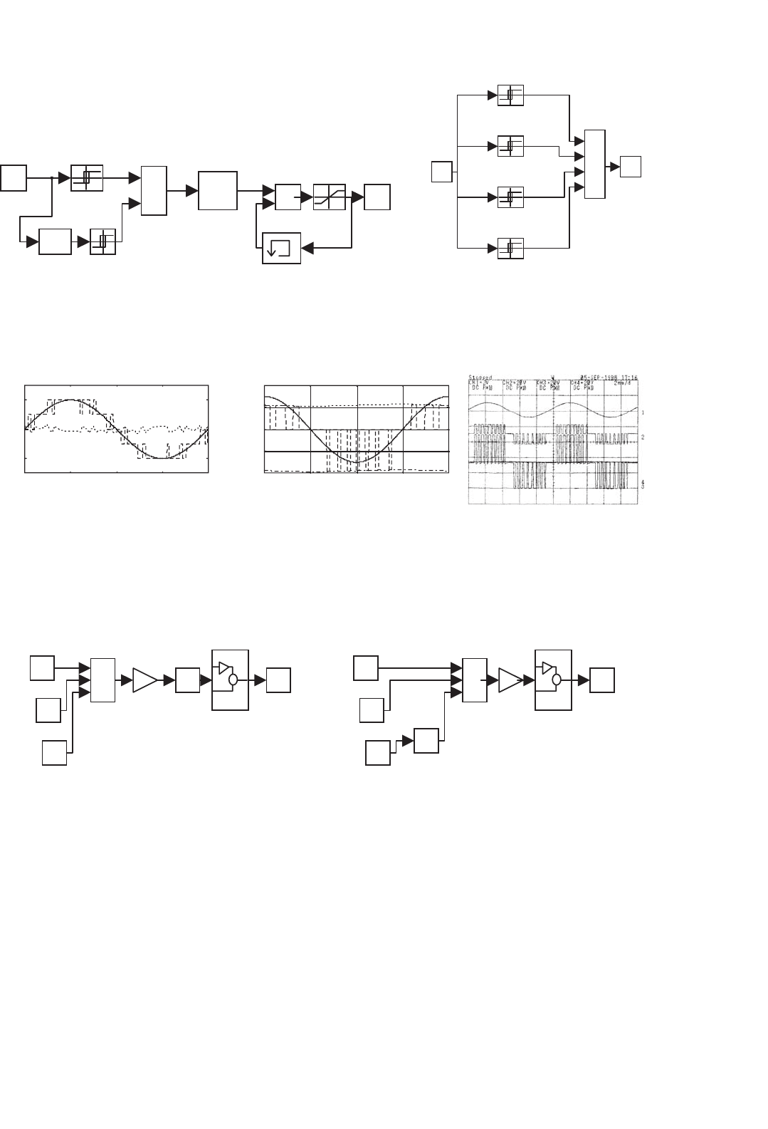
Three-phase n-level inverters (Fig. 34.58) are suitable
for high-voltage, high-power dc/ac applications, such
as modern high-speed railway traction drives, as the
controlled turn-off semiconductors must block only a
fraction (normally U
dc
/(n − 1)) of the total supply
voltage U
dc
.
This example presents a real-time modulator for the
control of the three output voltages and capacitor volt-
age equalization, based on the use of sliding mode and
space vectors represented in the α, β frame. Capacitor
voltage equalization is done with the proper selection of
redundant space vectors.
34.3.5.16 Output Voltage Control in Multilevel
Converters
To guarantee the topological constraints of this converter and
the correct sharing of the U
dc
voltage by the semiconduc-
tors, the switching strategy for the k leg (k ∈{1, 2, 3}) must
ensure complementary states to switches S
k1
and S
k3
. The same
restriction applies for S
k2
,S
k4
. Neglecting switching delays,
dead times, on-state semiconductor voltage drops, snubber
networks, and power supply variations, supposing small dead
times and equal capacitor voltages U
C1
= U
C2
= U
dc
/2,
and using the time-dependent switching variable γ
k
(t), the
leg output voltage U
k
(Fig. 34.58) will be U
k
= γ
k
(t)U
dc
/2,
with
γ
k
(t) =
1ifS
k1
∧S
k2
are ON ∧ S
k3
∧S
k4
are OFF
0ifS
k2
∧S
k3
are ON ∧ S
k1
∧S
k4
are OFF
−1ifS
k3
∧S
k4
are ON ∧ S
k1
∧S
k2
are OFF
(34.150)
The converter output voltages U
Sk
of vector U
S
can be
expressed
U
S
=
2/3 −1/3 −1/3
−1/3 2/3 −1/3
−1/3 −1/3 2/3
γ
1
γ
2
γ
3
U
dc
2
(34.151)
The application of the Concordia transformation U
S1,2,3
=
[C] U
Sα,β,o
(Eq. (34.152) to Eq. (34.151))
U
S1
U
S2
U
S3
=
2
3
·
101/
√
2
−1/2
√
3/2 1/
√
2
−1/2 −
√
3/2 1/
√
2
U
Sα
U
Sβ
U
So
(34.152)
gives the output voltage vector in the α, β coordinates U
S
α,β
:
U
S
α,β
=
U
Sα
U
Sβ
=
√
2/3
1 −1/2 −1/2
0
√
3/2 −
√
3/2
1
2
3
U
dc
2
=
α
β
U
dc
2
(34.153)
where
1
=
2
3
γ
1
−
1
3
γ
2
−
1
3
γ
3
;
2
=
2
3
γ
2
−
1
3
γ
3
−
1
3
γ
1
;
3
=
2
3
γ
3
−
1
3
γ
1
−
1
3
γ
2
(34.154)
34 Control Methods for Switching Power Converters 983
U
dc
i
dc
i
U
C
1
U
C
2
i
C
1
i
C
2
~
~
~
L
R
u
e
1
U
s
1
U
s
2
L
R
U
s
3
L
R
i
1
i
2
i
3
U
12
U
23
U
31
S
11
S
12
S
13
S
14
S
21
S
22
S
23
S
24
S
31
S
32
S
33
S
34
C
1
C
2
u
e
2
u
e
3
U
1
U
2
U
3
I
1
I
2
I
3
I'
1
I'
2
I'
3
i
n
FIGURE 34.58 Three-phase, neutral point clamped, three-level inverter with IGBTs.
The output voltage vector in the α, β coordinates U
S
α,β
is
discontinuous. A suitable state variable for this output can be
its average value
¯
U
S
α,β
during one switching period:
¯
U
S
α,β
=
1
T
T
0
U
S
α,β
dt =
1
T
T
0
α,β
U
dc
2
dt (34.155)
The controllable canonical form is
d
dt
¯
U
S
α,β
=
U
S
α,β
T
=
α,β
T
U
dc
2
(34.156)
Considering the control goal
¯
U
S
α,β
=
¯
U
S
α,β
ref
and Eq. (34.91),
the sliding surface is
S(e
α,β
,t)=
ϕ
o=1
k
αβ
o
e
α,β
o
=k
α,β
1
e
α,β
1
=k
α,β
1
¯
U
S
α,β
ref
−
¯
U
S
α,β
=
k
α,β
T
T
0
U
S
α,βref
−U
S
α,β
dt =0 (34.157)
To ensure reaching mode behavior, and sliding-mode
stability (34.92), as the first derivative of Eq. (34.157),
˙
S(e
α,β
, t), is
˙
S(e
α,β
, t) =
k
α,β
T
U
S
α,βref
−U
S
α,β
(34.158)
The switching law is
S(e
α,β
, t) > 0 ⇒
˙
S(e
α,β
, t) < 0 ⇒ U
S
α,β
> U
S
α,βref
S(e
α,β
, t) < 0 ⇒
˙
S(e
α,β
, t) > 0 ⇒ U
S
α,β
< U
S
α,βref
(34.159)
This switching strategy must select the proper values
of U
s
α,β
from the available outputs. As each inverter leg
(Fig. 34.58) can deliver one of the three possible output volt-
ages (U
dc
/2; 0; −U
dc
/2), all the 27 possible output voltage
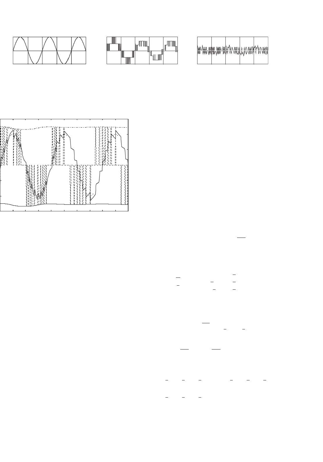
vectors listed in Table 34.3 can be represented in the α, β frame
of Fig. 34.59 (in per units, 1 p.u. = U
dc
). There are nine differ-
ent levels for the α space vector component and only five for
the β component. However, considering any particular value
of α (or β) component, there are at most five levels available
in the remaining orthogonal component. From the load view-
point, the 27 space vectors of Table 34.3 define only 19 distinct
space positions (Fig. 34.59).
To select one of these 19 positions from the control law
(34.157) and the switching law of Eq. (34.159), two five-level
hysteretic comparators (Fig. 34.53b) must be used (5
2
= 25).
Their outputs are the integer variables λ
α
and λ
β
, denoted λ
α,β
(λ
α
, λ
β
∈{−2; −1; 0; 1; 2}) corresponding to the five selectable
levels of
α
and
β
. Considering the sliding-mode stability,
λ
α,β
, at time step j + 1, is given by Eq. (34.160), knowing
their previous values at step j. This means that the output
level is increased (decreased) if the error and its derivative are
both positive (negative), provided the maximum (minimum)
output level is not exceeded.
(λ
α,β
)
j+1
= (λ
α,β
)
j
+1ifS(e
α,β
, t) >ε∧
˙
S(e
α,β
, t)
>ε∧ (λ
α,β
)
j
< 2
(λ
α,β
)
j+1
= (λ
α,β
)
j
−1ifS(e
α,β
, t) < −ε ∧
˙
S(e
α,β
, t)
< −ε ∧(λ
α,β
)
j
> −2
(34.160)
The available space vectors must be chosen not only to
reduce the mean output voltage errors, but also to guaran-
tee transitions only between the adjacent levels, to minimize
the capacitor voltage unbalance, to minimize the switching
frequency, to observe minimum on or off times if applicable,
and to equally stress all the semiconductors.
984 J. F. Silva and S. F. Pinto
TABLE 34.3 Vectors of the three-phase three-level converter, switching variables γ
k
, switch states s
kj
, and the corresponding output voltages, line
to neutral point, line-to-line, and α, β components in per units
Vector γ
1
γ
2
γ
3
S
11
S
12
S
13
S
14
S
21
S
22
S
23
S
24
S
31
S
32
S
33
S
34
U
1
U
2
U
3
U
12
U
23
U
31
U
sα
/U
dc
U
sβ
/U
dc
1 1 1 1110011001100U
dc
/2 U
dc
/2 U
dc
/2 0 0 0 0.00 0.00
2 1 1 0110011000110U
dc
/2 U
dc
/2 0 0 U
dc
/2 −U
dc
/2 0.20 0.35
3 11−1110011000011U
dc
/2 U
dc
/2 −U
dc
/2 0 U
dc
−U
dc
0.41 0.71
4 10−1110001100011U
dc
/2 0 −U
dc
/2 U
dc
/2 U
dc
/2 −U
dc
0.61 0.35
5 1 0 0110001100110U
dc
/2 0 0 U
dc
/2 0 −U
dc
/2 0.41 0.00
6 1 0 1110001101100U
dc
/2 0 U
dc
/2 U
dc
/2 −U
dc
/2 0 0.20 −0.35
7 1 −1 1110000111100U
dc
/2 −U
dc
/2 U
dc
/2 U
dc
−U
dc
0 0.41 −0.71
8 1 −1 0110000110110U
dc
/2 −U
dc
/2 0 U
dc
−U
dc
/2 −U
dc
/2 0.61 −0.35
9 1 −1 −1110000110011U
dc
/2 −U
dc
/2 −U
dc
/2 U
dc
0 −U
dc
0.82 0.00
10 0 −1 −10110001100110 −U
dc
/2 −U
dc
/2 U
dc
/2 0 −U
dc
/2 0.41 0.00
11 0 −1 00110001101100 −U
dc
/2 0 U
dc
/2 −U
dc
/2 0 0.20 −0.35
12 0 −1 10110001111000 −U
dc
/2 U
dc
/2 U
dc
/2 −U
dc
U
dc
/2 0.00 −0.71
13 0 0 10110011011000 0 U
dc
/2 0 −U
dc
/2 U
dc
/2 −0.20 −0.35
14 0 0 0011001100110000000 0.00 0.00
15 00−10110011000110 0 −U
dc
/2 0 U
dc
/2 −U
dc
/2 0.20 0.35
16 01−10110110000110 U
dc
/2 −U
dc
/2 −U
dc
/2 U
dc
−U
dc
/2 0.00 0.71
17 0 1 00110110001100 U
dc
/2 0 −U
dc
/2 U
dc
/2 0 −0.20 0.35
18 0 1 10110110011000 U
dc
/2 U
dc
/2 −U
dc
/2 0 U
dc
/2 −0.41 0.00
19 −1 1 1001111001100−U
dc
/2 U
dc
/2 U
dc
/2 −U
dc
0 U
dc
−0.82 0.00
20 −1 1 0001111000110−U
dc
/2 U
dc
/2 0 −U
dc
U
dc
U
dc
/2 −0.61 0.35
21 −11−1001111000011−U
dc
/2 U
dc
/2 −U
dc
/2 −U
dc
U
dc
0 −0.41 0.71
22 −10−1001101100011−U
dc
/2 0 −U
dc
/2 −U
dc
/2 U
dc
/2 0 −0.20 0.35
23 −1 0 0001101100110−U
dc
/2 0 0 −U
dc
/2 0 U
dc
/2 −0.41 0.00
24 −1 0 1001101101100−U
dc
/2 0 U
dc
/2 −U
dc
/2 −U
dc
/2 U
dc
−0.61 −0.35
25 −1 −1 1001100111100−U
dc
/2 −U
dc
/2 U
dc
/2 0 −U
dc
/2 U
dc
−0.41 −0.71
26 −1 −1 0001100110110−U
dc
/2 −U
dc
/2 0 0 −U
dc
/2 U
dc
/2 −0.20 −0.35
27 −1 −1 −1001100110011−U
dc
/2 −U
dc
/2 −U
dc
/2 0 0 0 0.00 0.00
25
24
21
20
19
18;23
17;22
1;14;27
2;15
3
4
6;11
5;10
7
8
9
12
13;26
16
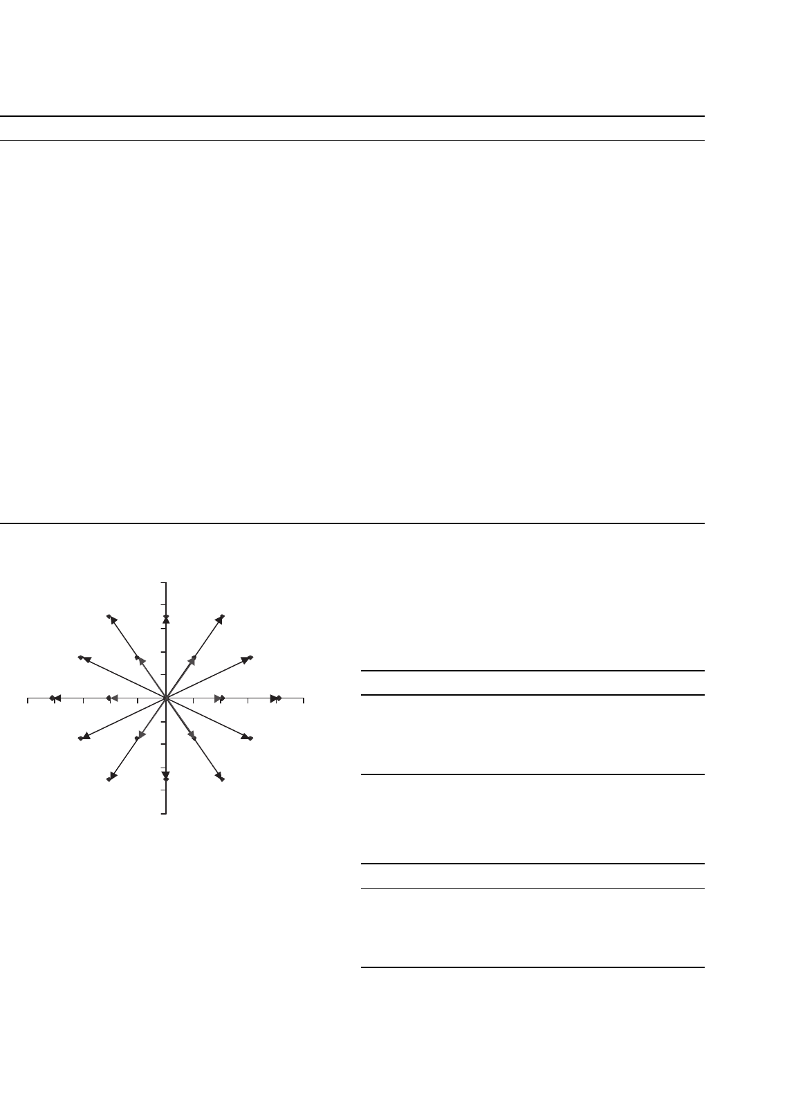
−1,0
−0,8
−0,6
−0,4
0,2
0,4
0,6
0,8
1,0
−1,0 −0,8 −0,6 −0,4 0,2 0,4 0,6 0,8 1,0
alfa
beta
FIGURE 34.59 Output voltage vectors (1 to 27) of three-phase, neutral-
clamped three-level inverters, in the α, β frame.
Using Eq. (34.160) and the control laws S(e
α,β,t
)
Eq. (34.157), Tables 34.4 and 34.5 can be used to choose
the correct voltage vector in order to ensure stability, output
voltage tracking, and DC capacitor voltage equalization. The
vector with α, β components corresponding to the levels of the
TABLE 34.4 Switching table to be used if (U
C1
− U
C2
) >ε
eU
in
the inverter mode, or (U
C1
− U
C2
) < −ε
eU
in the regenerative mode,
showing vector selection upon the variables λ
α
, λ
β
λ
β
\λ
α
−2 −10 12
−2 25 25 12 7 7
−1 24 13 13;6 6 8
0 19 18 1;14;27 5 9
1 20 17 17;2 2 4
2 21 21 16 3 3
TABLE 34.5 Switching table to be used if (U
C1
− U
C2
) >ε
eU
in
the regenerative mode, or (U
C1
− U
C2
) < −ε
eU
in the inverter mode,
showing vector selection upon the variables λ
α
, λ
β
λ
β
/λ
α
−2 −10 1 2
−2 25 25 12 7 7
−1 24 26 26;11 11 8
0 19 23 1;14;27 10 9
1 20 22 22;15 15 4
2 21 21 16 3 3

34 Control Methods for Switching Power Converters 985
pair λ
β
, λ
α
is selected, provided that the adjacent transitions on
inverter legs are obtained. If there is no directly corresponding
vector, then the nearest vector guaranteeing adjacent transi-
tions is selected. If a zero vector must be applied, then, one of
the three zero vectors (1, 14, 27) is selected, to minimize the
switching frequency. If more than one vector is the nearest,
then, one of them is selected to equalize the capacitor voltages,
as shown next.
34.3.5.17 DC Capacitor Voltage Equalization
The discrete values of λ
α,β
allow 25 different combinations. As
only 19 are distinct from the load viewpoint, the extra ones can
be used to select vectors that are able to equalize the capacitor
voltages (U
C1
= U
C2
= U
dc
/2).
Considering the control goal U
C1
= U
C2
, since the first
derivatives of U
C1
and U
C2
Eq. (34.161) directly depend on
the γ
k
(t) control inputs, from Eq. (34.91) the sliding surface
is given by Eq. (34.162), where k
U
is a positive gain.
d
dt
U
C1
U
C2
=
−
γ
1
(1+γ
1
)
2C
1
−
γ
2
(1+γ
2
)
2C
1
−
γ
3
(1+γ
3
)
2C
1
1
C
1
−
γ
1
(1−γ
1
)
2C
2
−
γ
2
(1−γ
2
)
2C
2
−
γ
3
(1−γ
3
)
2C
2
1
C
2
i
1
i
2
i
3
i
dc
(34.161)
S(e
Uc
,t)=k
U
e
Uc
(t)=k
U
(U
C1
−U
C2
)=0 (34.162)
The first derivative of U
C1
− U
C2
(the sliding surface) is
(Fig. 34.58 with C
1
= C
2
= C):
d
dt
e
Uc
=
i
C1
C
1
−
i
C2
C
2
=
i
n
C
=
(γ
2
3
−γ
2
1
)i
1
+(γ
2
3
−γ
2
2
)i
2
C
(34.163)
To ensure reaching mode behavior and sliding-mode stabil-
ity, from Eq. (34.92), considering a small enough e
Uc
(t) error,
ε
eU
, the switching law is
S(e
Uc
, t) >ε
eU
⇒
˙
S(e
Uc
, t) < 0 ⇒ i
n
< 0
S(e
Uc
, t) < −ε
eU
⇒
˙
S(e
Uc
, t) > 0 ⇒ i
n
> 0
(34.164)
From circuit analysis, it can be seen that vectors {2, 5, 6, 13,
17, 18} result in the discharge of capacitor C
1
, if the converter
operates in inverter mode, or in the charge of C
1
, if the con-
verter operates in boost-rectifier (regenerative) mode. Similar
reasoning can be applied for vectors {10, 11, 15, 22, 23, 26}
and capacitor C
2
, since this vector set give i
n
currents with
opposite sign relatively to the set {2, 5, 6, 13, 17, 18}. There-
fore, considering the vector [ϒ
1
, ϒ
2
]=[(γ
2
1
−γ
2
3
), (γ
2
2
−γ
2
3
)]
the switching law is:
IF (U
C1
−U
C2
) >ε
eU
THEN
IF the candidate vector from {2, 5, 6, 13, 17, 18}
gives (ϒ
1
i
1
+ϒ
2
i
2
) > 0, THEN choose the vector
according to λ
α,β
on Table 34.4;
ELSE, the candidate vector of {10, 11, 15, 22, 23,
26} gives (ϒ
1
i
1
+ϒ
2
i
2
) > 0, the vector being
chosen according to λ
α,β
from (table 34.5)
IF (U
C1
−U
C2
) < −ε
eU
THEN
IF the candidate vector from {2, 5, 6, 13, 17, 18}
gives (ϒ
1
i
1
+ϒ
2
i
2
) < 0, THEN choose the vector
according to λ
α,β
on Table 34.4;
ELSE, the candidate vector of {10, 11, 15, 22, 23,
26} gives (ϒ
1
i
1
+ϒ
2
i
2
) < 0, the vector being
chosen according to λ
α,β
from (table 34.5)
For example, consider the case where U
C1
> U
C2
+ ε
eU
.
Then, the capacitor C
2
must be charged and Table 34.4 must
be used if the multilevel inverter is operating in the inverter
mode or Table 34.5 for the regenerative mode. Additionally,
when using Table 34.4, if λ
α
=−1 and λ
β
=−1, then vector
13 should be used.
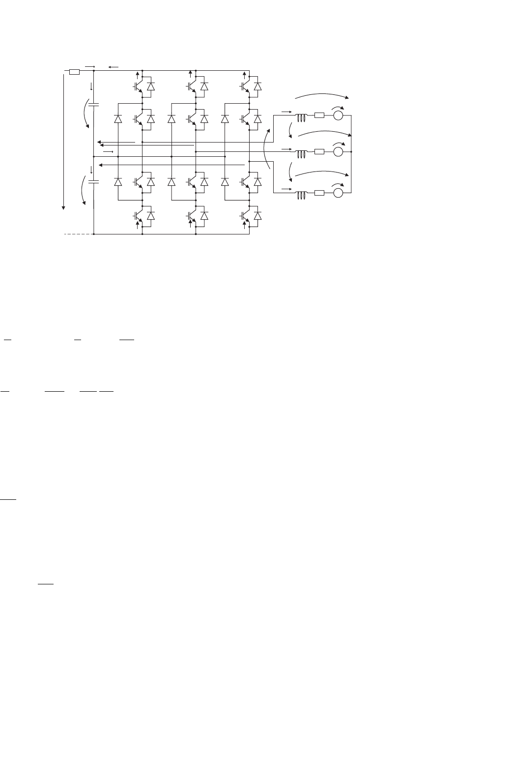
Experimental results shown in Fig. 34.61 were obtained with
a low-power, scaled down laboratory prototype (150 V, 3 kW)
of a three-level inverter (Fig. 34.60), controlled by two four-
level comparators, plus described capacitor voltage equalizing
procedures and EPROM-based lookup Tables 34.3–34.5. Tran-
sistors IGBT (MG25Q2YS40) were switched at frequencies
near 4 kHz, with neutral clamp diodes 40HFL, C
1
≈ C
2
≈
20 mF. The load was mainly inductive (3 ×10 mH, 2 ).
The inverter number of levels (three for the phase voltage
and five for the line voltage), together with the adjacent tran-
sitions of inverter legs between levels, are shown in Fig. 34.61a
and, in detail, in Fig. 34.62a.
The performance of the capacitor voltage equalizing strat-
egy is shown in Fig. 34.62b, where the reference current of
phase 1 and the output current of phase 3, together with the
power supply voltage (U
dc
≈ 100 V) and the voltage of capaci-
tor C
2
(U
C2
), can be seen. It can be noted that the U
C2
voltage
is nearly half of the supply voltage. Therefore, the capacitor
voltages are nearly equal. Furthermore, it can be stated that
without this voltage equalization procedure, the three-level
inverter operates only during a brief transient, during which
one of the capacitor voltages vanishes to nearly zero volt and
the other is overcharged to the supply voltage. Figure 34.61b
shows the harmonic spectrum of the output voltages, where
the harmonics due to the switching frequency (≈4.5 kHz) and
the fundamental harmonic can be seen.
986 J. F. Silva and S. F. Pinto
U
c1
U
c2
3 Level Converter
AC
Load
EPROM
1,2 ->αβ
U
dc
+
−
+
−
+
−
u
β
ref
us
α
us
β
u
2
u
1
S
x1
S
x2
S
x3
S
x4
D
x1
D
x2
Control
Board
5 Levels
5 Levels
Sgn(Uc1-Uc2)
Sgn(ϒ
1
i
1
-ϒ
2
i
2
)
u
α
ref
Regula
tor
i
2
i
1
Regulator
FIGURE 34.60 Block diagram of the multilevel converter and control
board.
34.3.5.18 On-line Output Current Control in
Multilevel Inverters
Considering a standard inductive balanced load (R, L) with
electromotive force (u) and isolated neutral, the converter
output currents i
k
can be expressed
U
Sk
= Ri
k
+L
di
k
dt
+u
ek
(34.165)
Now analyzing the circuit of Fig. 34.58, the multilevel
converter switched state-space model can be obtained:
d
dt
i
1
i
2
i
3
=−
R/L 00
0 R/L 0
00R/L
i
1
i
2
i
3
−
1/L 00
01/L 0
001/L
u
e1
u
e2
u
e3
+
1
/L
2
/L
3
/L
U
dc
2
(34.166)
0.00 8.00 kHz
T
3
2
1
T
U
1
U
3
U
13
(
a
)(
b
)
CH1 = 50 V
CH2 = 50 V
3:Math
1-2
CH4 = 20 mV
DC
10:1
DC
10:1
DC
1:1
NORM:500 ks/s
2 ms / div
(2 ms / div)
FIGURE 34.61 (a) Experimental results showing phase and line voltages and (b) harmonic spectrum of output voltages.
The application of the Concordia matrix Eq. (34.152) to
Eq. (34.166), reduces the number of the new model equations
(Eq. (34.167)) to two, since an isolated neutral is assumed.
d
dt
i
α
i
β
=−
R/L 0
0 R/L
i
α
i
β
−
1/L 0
01/L
u
eα
u
eβ
+
1/L 0
01/L
U
Sα
U
Sβ
(34.167)
The model Eq. (34.167) of this multiple-input multiple-
output system (MIMO) with outputs i
α
, i
β
reveals the control
inputs U
Sα
, U
Sβ
, dependent on the control variables γ
k
(t).
From Eqs. (34.167) and (34.91), the two sliding surfaces
S(e
α,β,
t) are
S(e
α,β
, t) = k
α,β
(i
α,βref
−i
α,β
) = k
α,β
e
α,β
= 0 (34.168)
The first derivatives of Eq. (34.167), denoted
˙
S(e
α,β,t
), are
˙
S(e
α,β
, t) = k
α,β
(
˙
i
α,βref
−
˙
i
α,β
)
= k
α,β
˙
i
α,βref
+RL
−1
i
α,β
+u
eα,β
L
−1
−U
Sα,β
L
−1
(34.169)
Therefore, the switching law is
S(e
α,β
,t)> 0⇒
˙
S(e
α,β
,t)< 0⇒U
S
α,β
>L
˙
i
α,βref
+Ri
α,β
+u
eα,β
S(e
α,β
,t)< 0⇒
˙
S(e
α,β
,t)> 0⇒U
S
α,β
<L
˙
i
α,βref
+Ri
α,β
+u
eα,β
(34.170)
These switching laws are implemented using the same α, β
vector modulator described above in this example.
Figure 34.63a shows the experimental results. The multi-
level converter and proposed control behavior are obtained
for step inputs (4 to 2A) in the amplitude of the sinus refer-
ences with frequency near 52 Hz (U
dc
≈ 150 V). Observe the
tracking ability, the fast transient response, and the balanced