Parinov I.A. Microstructure and Properties of High-Temperature Superconductors
Подождите немного. Документ загружается.

108 3 Experimental Investigations of HTSC
Deformation was estimated as [776] ε =6dΔl/L
2
and deformation rate as
˙ε =6dV
n
/L
2
,whereV
n
=Δl/t is the loading speed, d is the thickness tape,
L is the distance between supports. A test specimen is loaded consistently in
several sites. The AE signal activity was discontinuous in the form of single
bundles, characterizing non-uniformity of the fracture process or defect initi-
ation under loading, which was proper for brittle fracture.
First, a contribution in the AE activity from deformation of a silver sheath
was stated. For this, the tests of pure silver tapes with the same sizes and
conditions of loading, as for the tested Bi-2223/Ag tapes, have been carried
out. Moreover, it has been proved that loading device did not cause acoustic
noises. In order to confirm a character of fracture and correlation of the AE
activity with the sample damage during loading, a comparison was carried
out between the obtained test data and the experimental results (obtained by
A. A. Polyanskii [856] by MOI method [859]) of critical current I
c
and crit-
ical current density J
c
in magnetic fields directed along c-axis of the tapes.
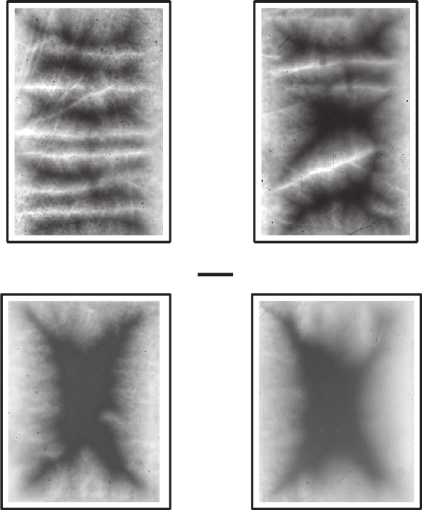
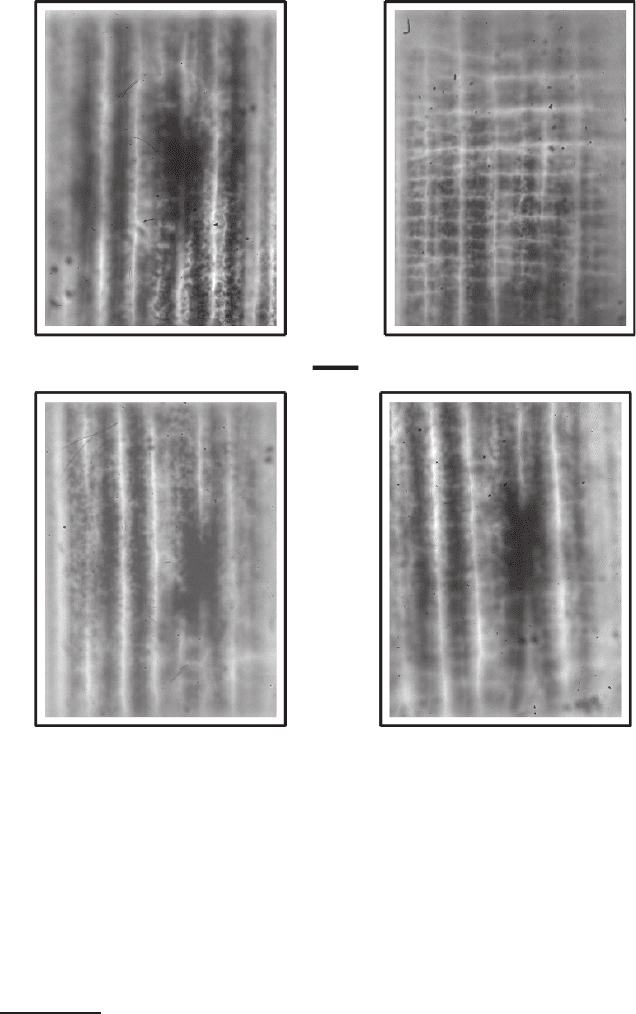
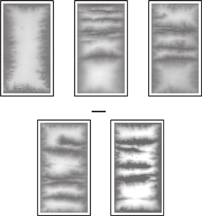
Magneto-optical images demonstrated pictures of the magnetic flux arrange-
ments directly in regions loaded for two regimes: zero field cooled (ZFC) and
field cooled (FC). In ZFC, the sample was cooled below T
c
in the absence of a
field, and then a field was applied. In the resulting image (Figs. 3.7 and 3.8)
the sample was shielding the magnetic field. For the FC regime, the sample
was cooled below T
c
in the presence of a magnetic field, and then the field
was turned off, so the sample was trapping magnetic flux (Fig. 3.9).
The test results for monocore tapes #1 and #3 and also for multi-
filamentary tape #2 by using the AE and MOI methods are presented in
Tables 3.1 and 3.2 and Figs. 3.7–3.9. As it follows from Table 3.1 and Figs. 3.7
and 3.8, in total, there is a good correlation between results obtained by the
above two methods. Moreover, for sample #2, a tendency of the damage
increasing with increasing strain and deformation rate is obvious. The corre-
lation of the results in the case of sample #3 (see Tables 3.2 and Fig. 3.9) is
less obvious. Based on the AE tests of this sample, the following conclusions
are possible:
(1) At sites 2 and 3 with the smallest critical current, AE signals were also
observed. The site 3 (with the smallest critical current) was loaded in
the tests twice. It may be assumed that during first loading (when electric
hindrances were observed), a sample cracking was initiated that was forced
at repeated loading.
(2) An absence of AE signals at the sites 1 and 4 (at the existence of cracks,
revealed by the MOI method) is related with the possible absence of a
good acoustic contact of the sample with the transducer or/and due to
the cracks that could be formed at the following accompaniment of the
sample (i.e., at marking of the sample, its straightening or/and in the
following measurements).
Additionally, the AE tests of the Bi-2223/Ag monocore tapes were carried
out with the following measurement of I
c
(at 77 K). At the testing of three
3.1 Experimental Methods of HTSC Investigations 109
1 mm
(a)
(c) (d)
(b)
Fig. 3.7. Magneto-optical images of the monocore tape #1, ZFC regime (T = 13 K,
H = 600 Oe): (a) site 1 (two-side bending), six cracks are seen; (b)site2,3cracks
are seen; (c)site3,nocracks;and(d) site 4, weak defects [820]
samples with different strain rates (one test for every sample) there is correla-
tion between changes of the strain rate and critical current. We obtained the
critical currents I
c
= 31, 24 and 18 A for deformable samples (for initial un-
strained sample I
c
= 39 A). They corresponded to strain rates: ˙ε/d =0.00030,
0.00049 and 0.00054(s mm)
−1
, normalized in the thickness, at visible absence
of the dependence on strain. Corresponding correlation was also observed for
acoustic emission.
110 3 Experimental Investigations of HTSC
1 mm
(a)
(c)
(d)
(b)
Fig. 3.8. Magneto-optical images of the multi-filamentary tape #2, ZFC regime
(T = 13 K, H = 1200 Oe): (a) initial unstrained tape; (b) site 1, 10–12 great cracks
are seen; (c)site2,nocracks;(d) site 3, some cracks are possible [820]
Thus, an increase of the strain rate caused a forcing of the AE activity,
accompanying greater microdamage and corresponding diminishes of critical
current. Hence, it is necessary to take into account the sample strain rate at
evaluation of the superconducting tape damage, additionally to the sample
deformation.
1
1
The sample strain is only taken into account at mechanical treatment of the
deformational behavior of structure-sensitive properties, usually.
3.1 Experimental Methods of HTSC Investigations 111
(a)
(b)
(c)
(d)
(e)
1 mm
Fig. 3.9. Magneto-optical images of the monocore tape #3, FC regime at
H=600Oe(T=12K,H=0Oe):(a) initial unstrained tape; (b) site 1, 4–5 great
cracks are seen; (c) site 2, 3–4 great cracks are seen; (d) site 3, 5 great cracks are
seen; (e) site 4, 4–5 great cracks are seen [820]
Based on the above tests, it could be concluded that AE method is suitable
to estimate the microdamage formation and propagation during Bi-2223/Ag
tape bending. An improvement of the test results may be related to using the
designed interference method [817] and the created optic-holographic device
for estimation of small displacements [705, 818].

112 3 Experimental Investigations of HTSC
Table 3.1. Test results for the samples #1 and #2 obtained by the AE and MOI methods
No. of
site
Δl
(mm)
V
n
(mm/s)
ε/d
(mm
−1
)
˙ε/d
(s mm)
−1
˙
N (imp/s) ΣN
(imp)
ΣA
(×10
−7
m)
P
m
(g) MOI data
#1,
site 1
3 0.1 0.0147 0.00049 – – – 5 –
#1,
site 1
a
1.5 0.06 0.0073 0.00029 80 (in 6 bundles) 800 0.2 5 6 cracks
#1,
site 2
2.4 0.15 0.0118 0.00074 130 (in 3 bundles) 400 – 5 3 cracks
#1,
site 3
2.9 0.2 0.0142 0.00098 – – – 5 No cracks
#1,
site 4
2.9 0.26 0.0142 0.00127 1500 (in 1 bundle) 3000 0.6 5 Weak defects
#2,
site 1
3 0.2 0.0147 0.00098 ≈ 1300 (in 1 bundle) 4000 3 80 10–12 great cracks
#2,
site 2
1.4 0.06 0.0069 0.00029 – – – 75 No cracks
#2,
site 3
2.9 0.08 0.0142 0.00039 150 (in 4 bundles) 600 0.2 80 some cracks are
possible
a
At second loading of considered site from the opposite side

3.1 Experimental Methods of HTSC Investigations 113
Table 3.2. Test results of AE and critical current for sample #3
Property Site 1 Site 2 Site 3 Site3
a
Site 4
Δl (mm) 6 6.5 4.3 6.5 6.5
V
n
(mm/s) 0.33 0.23 0.3 0.3 0.26
ε/d (mm
−1
) 0.0294 0.0319 0.0211 0.0319 0.0319
˙ε/d (s mm)
−1
0.00162 0.00113 0.00148 0.00148 0.00127
˙
N (imp/s) – 300 (in 9 bundles) AE with electric
hindrances
400 (in 1 bundle) –
ΣN (imp) – 1000 400 –
ΣA(×10
−7
m) – 1 0.2 –
P
m
(g)1418182022
I
c
(A) 23 18 – 14 21
J
c
(kA/cm
2
) 15.6 12.2 – 9.5 14,2
AE data No AE There are active
defects
AE is not distin-
guished
Weak AE No AE
a
At second loading of considered site from the same side. For original no-deformed edge of the sample placed at the outer side of
supports at the first loading, the measured critical current had the following values: I
c
=45AandJ
c
=30.6kA/cm
2
(at T =77K).
Maximum thickness of Bi-2223 core is equal to 60 μm, and S =1.47 × 10
−3
cm
2
is the cross-section area
114 3 Experimental Investigations of HTSC
3.2 Intergranular Boundaries in HTSC
The properties of high-angle grain boundaries are believed to control the
macroscopic J
c
(H) characteristics of all polycrystalline HTSC. This control
occurs because most high-angle grain boundaries act like barriers to the cur-
rent and have electromagnetic properties, such as Josephson junction-like
properties [205]. On the other hand, in the melt-processed polycrystalline
YBCO, actual currents can penetrate through intergranular boundaries mis-
oriented up to 30
◦
and more. So, HTSC properties are connected closely with
distribution of the intergranular boundary misorientations [205, 649].
From both the high-field flux-pinning viewpoint and low-field, Josephson
junction-based electronics viewpoint, there is strong motivation to develop a
detailed picture of the grain boundary structure and microstructure and to
describe their effects on the electromagnetic properties of the grain bound-
aries. The superconducting coherence length, ξ, defines the grain boundary
thickness that may be penetrated by the supercurrent. In this case, barriers
with thickness up to a few coherence lengths can still show superconducting
coupling, albeit of reduced strength. At the same time, the grain bound-
aries in HTSC are defects with thickness in the 0.5–1.0 nm range, indeed,
approaching ξ [40, 582]. Super-short coherence length and great values of n
in the power dependence of E–J (where E is the electric field intensity and
J is the current density) proper for HTSC [370, 372], sign, that the defects
with size of some nanometers can prevent supercurrent and create obstacles
with effective size, that is considerably higher than nominal size of defect.
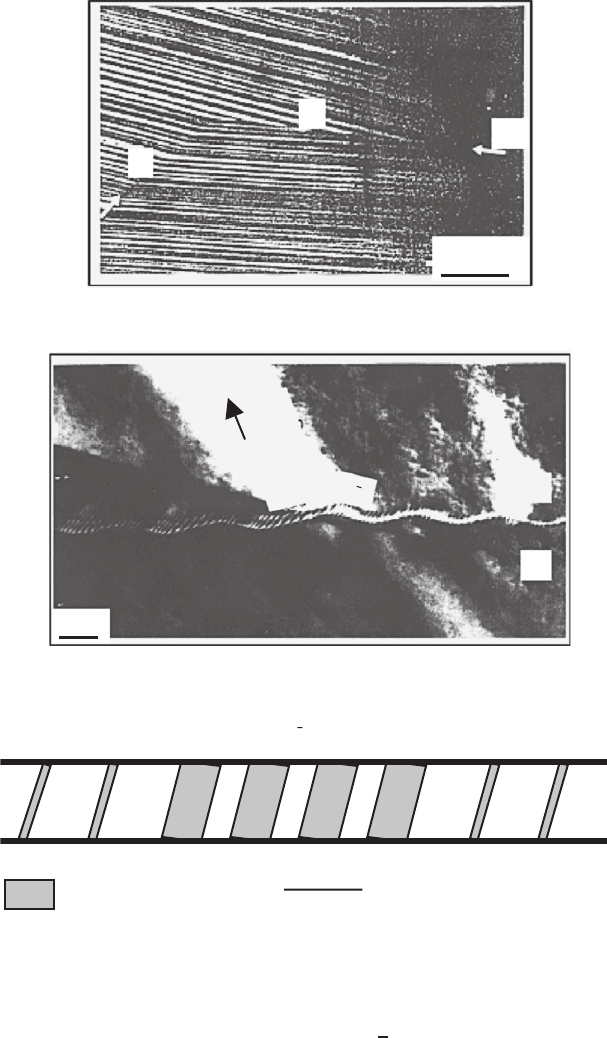
There are other planar defects, causing magnetic flux pinning and supercur-
rent percolation in HTSC, namely (i) twinning in YBCO [288, 593, 622],
(ii) stacking faults [272, 677], (iii) colonies of low-angle c-axis intercrystalline
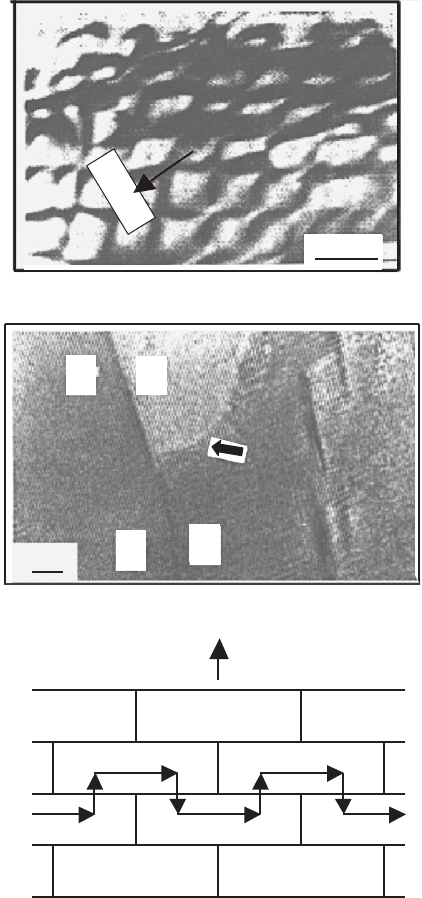
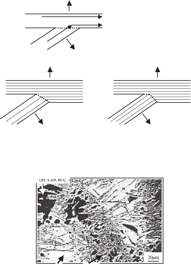
boundaries [272, 677, 1096], (iv) twist intergranular boundaries of the “brick
wall” type [104] and low-angle a-, b-axis boundaries of the “railway switch”
type [1186] in BSCCO, (v) overgrowth of Bi-2223 phase into Bi-2212 phase
[559], (vi) overgrowth of superconducting phase into silver sheath [887], (vii)
amorphous and normal (non-superconducting) phases [289], (viii) voids, mi-
crocracks and other crack-like defects, which are proper for all oxide supercon-
ductors [403, 743], (ix) macrodefects into Josephson junctions [1014], and also
various dislocation networks [634], discussed in detail below. Different types of
planar defects causing the structure-sensitive properties of HTSC, are shown
in Fig. 3.10.
Polycrystalline YBCO samples can be divided into two broad classes, ac-
cording to microstructure features, namely (i) specimens heated above peri-
tectic temperature with the aim of obtaining oblong well-orientated grains
[14] and (ii) samples sintered with grain structure that is near to equal-axes
one [975]. The experimental studies relate to investigation of both individual
isolated grain boundaries and polycrystalline samples with averaged effects of
great number of the intercrystalline boundaries. Both test types often sup-
plement each other. So, the study of high-angle boundaries in YBCO thin
3.2 Intergranular Boundaries in HTSC 115
(a)
(b)
(c)
A
20
µm
GB
YBCO
B
g
200
130
221
1
2
50 nm
(221) Facet
Stacking Faults
Partial Dislocation
Fig. 3.10. Different types of planar defects in HTSC: (a) {110} twinning boundaries
in the 10
◦
-bicrystal of YBCO (A and B are the macroscopic facets) [1082]; (b)
diffraction contrast image of the spatial dislocation network configuration in grain
boundary (g = [200] is the diffraction vector), the dark and bright areas are associated
with long-range strain contrast in facet junctions [1079]; (c) schematic diagram,
showing the arrangement of dislocations in the (22
1) facet [1079]
116 3 Experimental Investigations of HTSC
AB
1
2
20 nm
c-axis
J
(f)
(e)
(d)
g = 100
100 nm
Fig. 3.10. (d) screw dislocation in twist intergranular boundary [1131]; (e) lattice
fringe image, showing examples of a twist grain boundary (grains A and B), a
low-angle c-axis tilt colony boundary (colonies 1 and 2) and a low-angle ab-axis tilt
colony boundary (arrow) [242]; (f) twist intergranular boundaries of the “brick wall”
type [1186]
3.2 Intergranular Boundaries in HTSC 117
(g)
c-axis
c-axis
Grain
Grain
The “railway switch” model with a
low-angle c-axis GB at the switch.
c-axis
c-axis
c-axis
c-axis
The “railway switch” model with
a low-angle c-axis GB at the
switch. A special switch structure,
containing no (001) plane.
The “railway switch” model with
a low-angle c-axis GB at the
switch. A general switch structure,
containing part of the (001) plane.
(h)
(Sr, Ca)CuO
2
Bi- 2212 Bi-2223
20µm
Fig. 3.10. (g) different models of the grain boundaries of the “railway switch” type
[1186]; (h) overgrowth of Bi-2223 phase into Bi-2212 phase [289]
