Litton C.W., . Reynolds D.C., Collins T.C. Zinc Oxide Materials for Electronic and Optoelectronic Device Applications
Подождите немного. Документ загружается.

although efficient electrically induced lasing awaits further improvements in the experi-
mental ability to grow high quality p-type ZnO material. Nonetheless, over the past
decade, researchers world-wide have made substantial theoretical and experimental
progress concerning the p-type dopabi lity of ZnO, with 10
17
cm
3
range hole concentra-
tions now plausibly achieved with material stability persisting for over 1 year, and with
isolated (though often controversial) reports of hole concentrations as high as 10
19
cm
3
even being reported from time to time. Finally, ZnO structures can be doped with transition
metal (TM) ions to form dilute magnetic materials, denoted (Zn,TM)O, which can form a
ferromagnetic state, an antiferromagnetic state as well as a general spin glass. The
important point is that the Curie temperature (T
C
) can be above room temperature. Such
above-room-temperature anti- and ferromagnetic states form the basis for novel charge-
based, spin -based, or even mixed spin- and charge-based devices which, collectively, are
known as “spintronic” devices.
1.1.2 Organization of Chapter
The remainder of this chapter is organized as follows. In Section 1.2, a theoretical overviewof
the fundamental band structure of ZnO near the zone center is presented. The discussion
includes the long-standing controversy over the symmetry-ordering of the valence bands at
the G point. Next, in Section 1.3, the optical prope rties of intrinsic ZnO are reviewed, with
particular emphasis on the excitons. Also presented in this same section are a discussion of the
interaction of light, magnetic field, and strain field, as three examples of the general types of
calculations done for excitons in ZnO, as well as a discussion of spatial resonance dispersion
(Section 1.3.4) in which the polariton, a combined state arising out of the mixing of an exciton
and light, plays a particularly important role. The electrical properties of ZnO are consi dered
next in Section 1.4, including a discussion of intrinsic along with n-type and p-type ZnO. In
particular, the important question of p-type dopability is discussed in detail in Section 1.4.3.
For the implementation of optoelectronic devices, onewill need Schottky barriers and ohmic
contracts; recent progress in these areas is presented in Section 1.4.4. For heterojunction-
based devices, band gap engineer ing will be required and this is considered in Section 1.5.
Finally, presented in Section 1.6 is the theoretical basis for the ZnO spintronic device. The
different models are based on the Heise nberg Spin Hamiltonian to describe the dilute
magnetic system (Zn,TM)O. One can investigate both the interaction of the carriers with
the magnetic moment of the TM as well as the TM–TM interactions. It is found that the
resulting Curie temperature can be above room temperature. Spintronic devices made of
(Zn,TM)O are expected to be faster and to consume less power since flipping the spin requires
10–50 times less power, and occurs roughly an order of magnitude faster, than does
transporting an electron through the channel of traditional field-effect transistors (FETs).
1.2 Band Structure
1.2.1 Valence and Conduction Bands
The general electronic structure of binary III–V and II–VI compounds form semiconduc-
tors with the valence band mostly derived from the covalent bonding orbitals (s and p).
2 Fundamental Properties of ZnO
While the conduction band consists of antibonding orbitals, as one moves further outward
from column IVof the periodic table, the binary compound semiconductors acquire a more
ionic character. These compounds form cubic (zinc blende) and hexagonal (wurtzite)
crystal structures, with ZnO crystallized in the wurtzite structure. The difference between
the zinc blende and wurtzite structures is that the zinc blende is cubic while the wurtzite is
a distortion of the cube in the [111] direction generally taken to be the z direction in the
wurtzite.
The ionicity effect puts more electrons on the group V or group VI atoms giving the
charge density more s and p characteristics of these elements in the valence band. It also
causes gaps at the edge of the Brillouin zone compared with just covalent bonding
materials. This translates into flatter bands across the Brillouin zone.
ZnO is a direct band gap semiconductor with valence-band maximum and conduction-
band minimum occurring at the G point. The conduction band is s-like from Zn at G and is
spin degenerate. The top three valence bands are p-like in character. They are split by the
spin-orbit interaction in both the zinc blende and wurtzite symmetry, while wurtzite
symmetry also has a crystal field splitting.
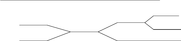
Figure 1.1 shows
[1]
the Quasi-cubic model
[2–4]
of the bottom of the con-duction band
and the top of the valence band. Assuming that one has both zinc blende and wurtzite and
that H
so
¼ DL S, one can write matrices of the form:
D 00
0 D 0
002D
0
@
1
A
ð1:1Þ
for zinc blende, using j ¼3/2 and j ¼1/2 eigenstates. For wurtzite the basis is rotated as
stated above, so that one has S
þ
a, S
b,S
a, S
þ
b, S
z
a, and S
z
b. This basis gives matrices
(including crystal field effects d) of the form
D 00
0 D i
ffiffiffiffiffiffi
2D
p
0 i
ffiffiffi
2
p
D d
0
@
1
A
: ð1:2Þ
Zincblende
Double Group Single Group
Wurtzite
Single Group Double Group
7c
Γ
8v
Γ
6c
Γ
1c
Γ
1c
Γ
Electron Conduction
Band
A
Hole
B
Hole
7v
Γ
4v
Γ
5v
Γ
1v
Γ
spin
orbit
crystal
field
7v
Γ
A Hole
B Hole
C Hole
7v
Γ
9v
Γ
spin
orbit
Figure 1.1 Structure and symmetries of the lowest conduction band and upmost valence
bands in ZnO compounds at the G point
Band Structure 3
Usingthevaluesobtained byThomas,
[5]
adifficultyarises. Ascanbe seeninEquation (1.3),
there are values of energy difference which can give a complex number for d:
d ¼
1
2
ð2E
1
þE
2
Þþ
1
2
ffiffiffiffiffiffiffiffiffiffiffiffiffiffiffiffiffiffiffiffiffiffiffiffiffiffiffiffiffiffiffiffiffiffiffi
E
2
2
2E
1
ðE
1
þE
2
Þ
q
ð1:3Þ
where E
1
is the energy difference between the G
9
excitons and G
7
exciton and E
2
is the
energy difference between the t wo G
7
excitons. In fact, using Thomas
[5]
numbers, d is a
complex number with G
9
being the top valence ba nd. T hi s difficulty can be surm oun ted
by assuming a negative spin-orbit splitting, which is different from all the other II–VI
compounds and GaN. The physical mechanism that could produce a negative spin-
orbit splitting was investigated by Cardona
[6]
for CuCl. In this zinc blende material, it w as
postulated that the valence band was formed from Cl wave functions, with a large
proportion of Cu w ave functions (Cu 4s3d). The inve rted nature of the CuCl indicates
that the Cu contributes a negative term to the spin-orbit splitting, since for this mat erial
the anion splitting is small and negative. Ca rd ona
6
estimated the “fraction” of the metal
wave function i n the valence band states by writing the spin-orbit splitting of the
compound as:
D ¼
3
2
aD
hal
ð1aÞD
met
½; ð1:4Þ
where a is the proportion of halogen in the wave function, D
hal
is the one-electron atomic
spin-orbit splitting parameter of the halogen and D
met
is one of the d-electrons of the metal.
This gave a ¼0.25 for CuCl. It was also presented that the energy interval between the
ground state of the Cu
þ
ion (3d
10
) and the first excited state (3d
9
, 4s) is 2.75 eV.
Returning to ZnO, one finds the Zn d-bands below the upper most p-like valence bands to
be greater than 7 eV.
[7–9]
This makes it very unlikely that one has muc h mixing at all.
Further, the d-band appeared to be relatively flat, noting again very little mixing. Also, the
availability of ZnO crystals in which intrinsic exciton transitions
[10]
are observed in
emission and their splitting in a magnetic field have led to a positive spin-orbit splitting of
16 meV. With this interpretation, the Quasi-cubic model
[2–4]
gives results in line with the
other II–VI compounds.
In order to investigate the valence band ordering of ZnO further, Lambrecht et al.
[11]
calculated the band structure of ZnO using a linear muffin-tin potential and a Kohn–Sham
local density approximation. The band gap at G was 1.8 eV compared with experiment of
3.4 eV and the Zn d-band was approximately 5 eV below the top of the valence band at G.
To correct for the band gap Reynolds et al.
[10]
rigidly shif ted the conduction band up to
match the experimental G-point gap (a shift of 1.624 eV).
As is seen from above in the Quasi-cubic model,
[2–4]
the spin-orbit magnitude and sign
are a function of the energy difference between the top of the valence and the 3d band of
Zn. It is found to be greater than 7 eV.
[7–9]
In Reynolds et al.,
[10]
the d-band was adjusted to
where the spin-orbit gave the right energy difference with the G
7
above the G
9
. The d band
was put at 6.25 eV below the top of the valence band. This led to a negative g-value and of
course a negative spin-orbit parameter. This in turn matched the experimental data given in
Hong et al.
[9]
but with a different interpretation of the splitting of the exciton lines. Thus,
there is no agre ement of the spin-orbit value for ZnO. In first principle electron structure
4 Fundamental Properties of ZnO

calculations, one has an accuracy only on the order of 100 meV whereas the splittings of
the levels in the top valence band are on the order of 10 meV!
1.3 Optical Properties
1.3.1 Free and Bound Excitons
The optical absorption (emission) of electromagnetic radiation in a ZnO crystal is
dependent on the matrix element
Z
Y
*
f
H
int
Y
i
dt ð1:5Þ
where
H
int
¼
eh
imc
A r: ð1:6Þ
Here, A is the vector potential of the radiation field and has the form
A ¼
^
njA
0
je
iðq rvtÞ
;
e is the electronic charge, m is the electron mass, c is the velocity of light,
^
n is a unit vector
in the direction of polarization, and q is the wave vector. Expanding the spatial part of A in
a series gives
H
int
X
¥
j¼0
H
j
int
ð1:7Þ
where
H
j
int
¼ðq rÞ
j
^
n r ð1:8Þ
and the dipole term is then the first term (i ¼0). The matrix element in Equation (1.5)
transforms under rotation like the triple direct product
G
f
G
j
r
G
i
: ð1:9Þ
The selection rules are then determined by which of the tripl e-direct-product matrix
elements in question do not vanish, where G
j
r
is the symmetry of the expansion term H
j
int
in
Equation (1.8).
The dipole moment operator for electric dipole radiation transforms like x, y,orz
dependent on the polarization. When the electric field vector E of the incident light is
parallel to the crystal axis of ZnO, the operator corresponds to the G
1
representation. When
it is perpendicular to the crystal axis, the operator corresponds to the G
5
representation.
Since the crystal has a principal axis, the crystal field removes part of the degeneracy of the
p-levels as seen in Figure 1.1. Including spin in the problem doubles the number of levels.
Since the conduction band at k ¼0 is the Zn (4s) level
[4,5]
it transforms as G
7
while the
k ¼0 at top of the valence band is made up of the O(2p) level and it splits into (p
x
,p
y
)G5
Optical Properties 5
and (p
z
)G1. When crossed with the spin one has
G
5
D
1=2
!G
7
þG
9
ð1:10Þ
G
1
D
1=2
!G
7
ð1:11Þ
as shown in Figure 1.1.
One of the light absorption (emission) intrinsic states is an exciton, which is made up of
a hole from the top of the valence band and an electron from the bottom of the conduction
band. These are excitations of the N-particle syst em whereas electron structure calcula-
tions are of the (N 1)-particle system. All solutions to the one-body calculations such as
the one-particle Green’s functions method do not contain the interaction of the excited
“particle” with the other “particles.” The more localized the excitation the more important
it is to include this interaction. The more localized the excitation is, the flatter the one-
electron bands, leading to heavier effective masses. This is turn leads to increased binding
energy of the elect ron–hole pair. In ZnO, the binding energy of the ground state exciton is
60 meV. Adding in the Coulomb term of the electron–hole pair gives a hydrogenically
bound pair. For the G
9
hole and G
7
electron one has
G
9
G
7
!G
5
þG
6
; ð1:12Þ
and for the G
7
hole and G
7
electron one has
G
7
G
7
!G
5
þG
1
þG
2
: ð1:13Þ
The G
5
and G
6
are doubly degenerate and the G
1
and G
2
are nondegenerate. The
Hamiltonian for the exciton becomes:
H¼H
e
þH
h
þH
int
; ð1:14Þ
where H
e
and H
h
are the Hamiltonian for the electron and the hole and H
int
is the
interaction between the electron and hole including Coulomb, exchange and correlation.
To first approximation one generally includes just the Coulomb term as noted above.
Equation (1.14) gives what are referred to as the “free” excitons.
There are several extrinsic effects which modify the excitons. Most notable of these in ZnO
are the bound complexes. One can have the exciton bound to an ionized donor or a neutral
donor. In the case of the ionized donor, one has the molecular attraction of the exciton to the
donor plus cent ral cell corrections. Forthe neutral donor,one has again the molecular binding
energy plus the ability of the neutral donor to be left in an excited state. Similar results are
obtained with the ionized acceptor or neutral acceptor. The method of calculating these
systems is to treat the system as a molecu lar system in the field of the crystal.
1.3.2 Effects of External Magnetic Field on ZnO Excitons
The case of an applied uniform magnetic field was developed by Wheeler and Dim-
mock
[12]
for the exciton in ZnO. It was assumed the electron bands are isotropic at least to
second order in k with only double spin degeneracy. The exciton equation is a simple
6 Fundamental Properties of ZnO

hydrogen Schr
€
odinger equation including effective-mass and dielectric anisotropies. It is
found that the mass anisotropy is small, allowing first-order perturbation calculations to be
made for the energy states as well as for the magnetic-field effects.
Sincethevalenceandconduction bandextremaare at k ¼0, thewavevectorof the lightthat
creates the exciton k will also represent the position of the exciton in k-space. Dividing the
momentum and spaces coordinates into the center-of-mass coordinates and the internal
coordinates, the exciton Hamiltoni an can be divided into seven terms as follows:
H¼H
1
þH
2
þH
3
þH
4
þH
k1
þH
k2
þH
k3
ð1:15Þ
H
1
¼
h
2
2m
1
m
x
@
2
@x
2
þ
@
2
@y
2
þ
1
m
z
@
2
@z
2
e
2
eh
1=2
x
2
þy
2
þh
1
z
2
1=2
ð1:16Þ
H
2
¼2iz
A
x
D
x
@
@x
þ
A
y
D
y
@
@y
þ
A
z
D
z
@
@z
ð1:17Þ
H
3
¼
e
2mc
2
A
2
x
m
x
þ
A
2
y
m
y
þ
A
2
z
m
z
!
ð1:18Þ
H
4
¼
z
2
X
i¼x;y;z
ðg
e
i
S
e
i
þg
h
i
S
h
i
ÞH
i
ð1:19Þ
H
k1
¼
ih
2m
K
x
D
x
@
@X
þ
K
y
D
y
@
@Y
þ
K
z
D
z
@
@Z
ð1:20Þ
H
k2
¼ z
K
x
m
x
A
x
þ
K
y
m
y
A
y
þ
K
z
m
z
A
z
!
ð1:21Þ
H
k3
¼
h
2
8m
K
2
x
m
x
þ
K
2
y
m
y
þ
K
2
z
m
z
!
; ð1:22Þ
where m is the free-electron mass and m
x
is the reduced effective mass of the exciton in the
x direction at G (m
x
¼m
y
). Also,
z ¼
eh
2mc
h ¼
e
z
e
x
ð1:23Þ
A ¼
1
2
ðH rÞð1:24Þ
Optical Properties 7

1
D
y
¼
m
m
*
ey
m
m
*
hy
!
: ð1:25Þ
The first term is the Hamiltonian for a hydrogenic system in the absence of external fields.
One could include the possibility of the mass and dielectric anisotropies. The second term
is an Ap term which leads to the linear Zeeman magnetic field term. In this term, the
momentum operator is p
i
2e A
i
/c where A
i
¼(1/2)H r
i
is the vector potential, H is the
magnetic field, and r
i
is the coordinate of the ith electron. The A
2
term is the diamagnetic
field term proportional to |H|
2
. The fourth term is the linear interaction of the magnetic
field with the spin of the electron and hole. If one has small effective reduced mass for the
electron and a large dielectric constant, the radii of the exciton states are much larger than
the corresponding hydrogen-state radii. Hence, the spin-orbit coupling is proportional to
r
3
and thus quite small, it is legitimate to write the magnetic field perturbations in the
Paschen–Back limit as done above.
The last three terms are the KP, KA, and K
2
terms; K is the center-of mass momentum.
Treating the KP to second order and adding the K
2
term, one can obtain an energy term
that appears like the center-of-mass kinetic energy. The K A term has little effect upon the
energy; however, it has very interesting properties. This term represents the quasi-electric
field that an observer riding with the center-of-mass of the exciton would experience
because of the magnet ic field in the laboratory. This quasi-field would produce a
Stark effect linear in H, and this would give rise to a maximum splitting interp retable
as a “g ” value.
1.3.3 Strain Field
The effective Hamiltonian formalism of Pikus
[13,14]
is of the form
H¼H
y0
þH
yp
þH
c
þH
int
; ð1:26Þ
Using the angular momentum operators J(L ¼1) gives
H
y0
¼ D
1
J
2
z
þD
2
J
z
s
z
þD
3
ðs
þ
J
þs
J
þ
Þ; ð1:27Þ
where D
1
is the crystal field splitting of the S
x
, S
y
bands from the S
z
band; D
2
is the spin-
orbit splitting of the j ¼3/2 bands from the j ¼1/2 band, and D
3
is a trigonal splitting of
the jj; m
j
i¼j
3
2
;
3
2
i bands from the j
3
2
;
1
2
i bands.
The operator H
yp
, which describes the interaction between the valence bands due to
strain, can be determined from symmetry considerations by combining the strain tensor
«
ij
with the angular momentum operators J and s:
H
yp
¼ðC
1
þC
3
J
2
z
Þ«
zz
þðC
2
þC
4
J
2
Z
Þð«
xx
þ«
yy
Þ
þC
5
ðJ
2
«
þ
þJ
2
þ
«
ÞþC
6
ð½J
z
J
þ
«
z
þ½J
z
J
«
þz
Þ
ð1:28Þ
Here,
«
¼ «
xx
«
yy
2i«
xy
«
z
¼ «
xz
i«
yz
; ð1:29Þ
8 Fundamental Properties of ZnO

and [J
i
J
j
] ¼(J
i
J
j
þJ
j
J
i
)/2. These operators then describe the mixing of the p-like valence
bands due to crystalline strain in the terms of material-dependent parameters (the C
i
’s).
The operator H
c
represents the conduction-band energy. Because of the G
1
symmetry of
the conduction band, the operator has the form
H
c
¼ E
c
þd
1
«
zz
þd
2
ð«
xx
þ«
xy
Þ: ð1:30Þ
H
int
is the Coulomb interaction plus the exchange term
H
int
¼ E
b
þ
1
2
js
h
s
e
ð1:31Þ
where in Equation (1.31)j denotes the usual exchange integral (not to be confused with
the usage of j as the angular momentum quantum number in the earlier equations).
The exchange term has off-diagonal matrix elements, and for example, removes the G
5
degeneracy. This leads to strain splittings, which are measured.
1.3.4 Spatial Resonance Dispersion
The excitons in ZnO interact with photons when the wave vector are essentially equal. The
energy denominator for exciton–photon mixing is small and the mixing becomes large.
These states are not to be consider ed as pure photon states or pure exciton states, but rather
mixed states. Such a mixed state is called a polariton. When there is a dispersion of the
dielectric constant, spatial dispersion has been invoked to explain certain optical effects of
the crystal. This causes more than one energy transport mechanism. Spatial dispersion
addresses the possibility that two different kinds of waves of the same energy and same
polarization can exist in a crystal differing only in wave vector. The one with an
anomalously large wave vector is an anomalo us wave. In the treatment of dispersion by
exciton theory, it was shown that if the normal modes of the system were allowed to
depend on the wave vector, a much higher-order equation for the index of refraction would
result. These new solutions occur whenever there is any curvature of the ordinary exciton
band in the region of large exciton–photon coupling. These results apply to the Lorentz
model as well as to quantum-mechanical models whenever there is a dependence of
frequency on wave vector.
The specific dipole moment of polarization of a crystal and the electric field intensity are
not in direct proportion. The two are related by a differential equation that resulted in
giving Maxwell equations of higher order. This leads to the existence of several waves of
the same frequency, polarization, and direction but with different indices of refraction. The
index of refraction becomes
n
2
¼
k
2
c
2
v
2
¼ e þ
X
j
4pða
0j
þa
2j
K
2
Þv
2
0j
v
2
0j
þðhv
0j
k
2
=m
*
v
2
ivGÞ
: ð1:32Þ
Here, the sum over j is to include the excitons in the frequency region of interest, and the
contributions from other oscillators are included in a background dielec tric constant e.In
Equation (1.32) the numerator and denominator have been expanded in powers of k,
keeping terms to order of k
2
, m
is the sum of the effective masses of the hole and electron
Optical Properties 9

that comprise the exciton, and v
0j
is the frequency of the j
th
oscillator at k ¼0. Eliminating
k
2
from Equation (1.32) and neglecting the linewidth of the oscillators, the equation
becomes
n
2
¼ e þ
X
j
4pða
0j
þa
2j
v
2
n
2
=c
2
Þv
2
0j
v
2
0j
þðhv
0j
v
2
n
2
=c
2
m
*
Þv
2
: ð1:33Þ
The sum is over excitons from the top two valence bands where the “allowed” excitons have
been included with a
0j
„ 0, a
2j
¼0 while the “forbidden” (because excitons are included
with a
0j
„ 0, a
2j
¼0). Equation (1.33) reduces to a polynomial in n
2
whose roots give the
wavelengths of the various “normal modes” for the transfer of energy within the crystal.
There is another structure seen in the spectra near the free exciton. This is the result of
the mixing of the exciton and photon with non crossing effects of the photon dispersion.
This creates a larger density of states where the mixing becomes strong enough to bind the
photon curve.
1.4 Electrical Properties
Electrically, ZnO is a transparent-conducting-oxide semiconductor which at room tem-
perature exhibits defect- or impurity-dominated n-type conductivity, even in nominally
undoped materials. This defect- or impurity-dominated conductivity is a consequence of
the large band gap
[15,16]
(3.3 eV at room temperat ure) combined with the unavoidable
presence of electrically active native defects and impurities with donor ionization energies
typically
[15]
10–100 meV at concentrations typically
[15]
10
15
–10
16
cm
3
. Furthermore,
while ZnO is readily doped n-type and carrier concentrations as high as 10
21
cm
3
are
achievable,
[17]
at present p-type doping remains challenging. Furthermore, for purposes of
utilizing ZnO-based materials for extending semiconductor optoelectronics further into
the UV, two of the biggest technological challenges will be to develop growth and device-
processing techniq ues to achieve control over p-type doping as well over metal/semicon-
ductor junction formation (including both Schottky and ohmic contacts) to both n-type and
p-type materials.
Most of what is known experimentally about the electronic properties of “pure” ZnO is
actually based on n-type specimens. The fundamental electronic transport properties of
nominally undoped and intentionally doped ZnO will be presented in Section 1.4.1. Next,
in Section 1.4.2, intentional n-type dopin g and dopants will be considered. Then, in
Section 1.4.3 will be discussed recent progress, both experimental and theoretical,
concerning the technologically important question of p-type dopability in ZnO. Finally,
recent progress on the fabrication of Schottky contacts to n-type, and of ohmic contacts to
both n-type and p-type ZnO, will be reviewed in Section 1.4.4.
1.4.1 Intrinsic Electronic Transport Properties
To date, available data concerning fundamental electronic properties of intrinsic, accu-
rately stoichiometric ZnO remains largely unknown.
[15]
In part this is because of the
10 Fundamental Properties of ZnO
historical unattainability of sufficiently high-quality materials, a consequence of the
difficulty (especially through bulk crystal-growth methods) in achieving adequate O
incorporation into the specimen. While such a circumstance may seem merely a
technological rather than a fundamental limitation, recent theoretical work
[18,19]
suggests
that the n-type character resulting from electrically active stoichiometric native point
defects such as vacancies, inter-stitials, and antisites,
[18]
as well as the unusually
nonamphoteric and donor-like character of unintentional but ever-present hydrogen,
[20]
may be inherent to ZnO, at least, to materials produced through the use of near-equilibrium
crystal growth methods. The question of p-type dopability shall be deferred to Sec-
tion 1.4.3. For the remainder of the present section we will consider the basic electronic
transport properties of nominally undoped ZnO which have been established experimen-
tally, along with modifications due to intentional n-type doping.
In general, electrical transport properties of ZnO are directionally depend ent due to
the anisotropy of its wurtzite crystal structure. For the case of nominally undoped (i.e.
residually n-type 10
16
cm
3
carrier concentration) ZnO, Figure 1.2 shows temperature-
dependent Hall mobility data for current transport both parallel and perpendicular to
the crystallographic c axis of bulk ZnO. As seen in Figure 1.2, the electron mobility attains
a peak value of 1000 cm
2
V
1
s
1
at a temperature of 50–60 K, and drops off approxi-
mately as the power law, T
p
for low temperatures and T
q
for high temperatures where p 3
and q 2 in Figure 1.2(a). The drop off at low temperature falls off faster than that
expected due to ionized-impurity scattering alone whereas that at high temperatures is at-
tributable primarily to the combination of acoustic-deformation-potential with polar-
optical-phonon scattering mechanisms.
[21]
The slight anisotropy observed in Hall mobility
data [compare Figure 1.2(a) and (b)] has been attributed exclusively to piezoelectric
scattering.
[15]
Also of interest is the electric-field dependence of the mobility. Figure 1.3 compares
theoretically obtained plots
[22]
of drift velocity (v
d
) vs electric field; resu lts predicted for
ZnO are contrasted with those for GaN, another direct-gap semiconductor having a closely
comparable band gap (E
GaN
g
3.4 eV) to ZnO. A comparison of the GaN and ZnO curves
at low field reveals that m
ZnO
G m
GaN
while at the same time the saturated drift velocities
obey the opposite relation: y
ZnO
Sat
Hy
GaN
Sat
. For hot-electron devices, whe re fields are high
and transport is nonohmic, it is y
sat
rather than m that can be the more important parameter
to device operation.
[23]
1.4.2 n-type Doping and Donor Levels
Intentional n-type doping is readily achieved through the use of column-III elements such
as Al, Ga, or In, or, column-VII elements such as Cl, F, or I. All of these sit substitutionally
on the appropriate cation or anion site and form reasonably shallow levels. In a 2001
review article, Look discusses the presence of three predominant donor levels in ZnO
appearing at approximately 30, 60, and 340 meV.
[23]
Among these, the 60 meV level is that
corresponding to effective mass theory (65 meV), whereas the 30 meV level was at the
time believed
[18,24]
to be due to interstitial Zn (Zn
i
) and no longer believed to be due to
the O vacancy (V
O
), which instead was thought to be a deep donor.
[18]
The identity of the
340 meV level was not established. Interestingly, also presented by Look in this same
review article
[23]
are some of his own temperature-dependent Hall mobility data which
Electrical Properties 11