Lallart M. Ferroelectrics: Characterization and Modeling
Подождите немного. Документ загружается.

Valence Band Offsets of ZnO/SrTiO
3
, ZnO/BaTiO
3
,InN/SrTiO
3
, and InN/BaTiO
3
Heterojunctions Measured by X-ray Photoelectron Spectroscopy 5
(E
B
CL
-E
B
V
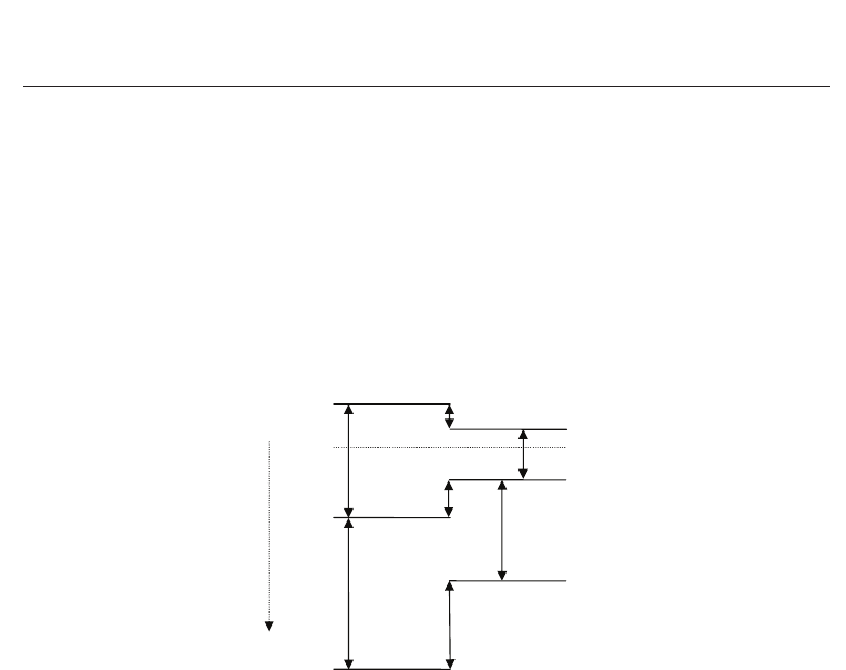
), respectively. By inspection of Fig. 1, it can be seen that
ΔE
V
(B − A)=(E
B
CL
− E
B
V
) − (E
A
CL
− E
A
V
)+ΔE
CL
(A − B).(8)
Thus, to apply XPS for ΔE
V
measurements, it is essential to determine the bulk semiconductor
material parameters (E
CL
-E
V
) for those semiconductors forming the heterojunctions. A
primary difficulty with measuring (E
CL
-E
V
) is the accurate determination of the E
V
position
in photoemission spectra. The most frequently employed method involves extrapolation of a
tangent line to the leading edge of the valence band spectrum to the energy axis, this intercept
is defined as E
V
. Substituting these values to Eq. 8, the VBO of heterojunction A/B can be
obtained.
increasing E
B
BA
E
CL
B
E
c
A
E
v
A
E
CL
A
E
c
B
E
v
B
E
g
B
E
g
A
(E
CL
-E
v
)
A
(E
CL
-E
v
)
B
ǻE
c
ǻE
v
ǻE
CL
E
B
=0
E
F
Fig. 1. Schematic energy band diagram illustrating the measurement of VBO by XPS.
3. Experimental
Several samples, bulk commercial (001) STO, (111) STO and (001) BTO substrates, thick
(several hundred nanometers) and thin (about 5 nm) ZnO and InN layers grown on the
commercial STO and BTO substrates were studied in this work. To get a clean interface,
the STO and BTO substrates were cleaned with organic solvents and rinsed with de-ionized
water sequentially before loading into the reactor. The thick and thin heterostructures of
ZnO/STO, ZnO/BTO, InN/STO and InN/BTO were deposited by MOCVD. More growth
condition details of the ZnO and InN layers can be found in our previous reports (Jia et al.,
2008; 2009a;b; 2010a;b; 2011; Li et al., 2011).
XPSs were performed on ThermoFisher ESCALAB 250, PHI Quantera SXM, and VG MKII
XPS instruments with AlKα (h ν=1486.6 eV) as the x-ray radiation source, which had been
carefully calibrated on work function and Fermi energy level (E
F
). Becauseallthesamples
were exposed to air, there must be some impurities (e.g., oxygen and carbon) existing in the
sample surface, which may prevent the precise determination of the positions of the valence
band maximum (VBM). To reduce the undesirable effects of surface contamination, all the
samples were cleaned by Ar
+
bombardment at a low sputtering rate to avoid damage to the
samples. After the bombardment, peaks related to impurities were greatly reduced, and no
new peaks appeared. Because a large amount of electrons are excited and emitted from the
sample, the sample is always positively charged and the electric field caused by the charge can
affect the measured kinetic energy of photoelectron. Charge neutralization was performed
309
Valence Band Offsets of ZnO/SrTiO
3
, ZnO/BaTiO
3
,
InN/SrTiO
3
, and InN/BaTiO
3
Heterojunctions Measured by X-Ray Photoelectron Spectroscopy

6 Will-be-set-by-IN-TECH
with an electron flood gun and all XPS spectra were calibrated by the C 1s peak at 284.8 eV
from contamination to compensate the charge effect. Since only the relative energy position in
each sample is needed to determine the VBO, the absolute energy calibration for a sample
has no effect on the ultimate result. The surfaces of samples were examined initially by
low-resolution survey scans to determine which elements were present. Very high-resolution
spectra were acquired to determine the binding energy of core level (CL) and the valence
band maximum energy in the survey spectra. All the CL spectra were fitted to Voigt (mixed
Lorentz-Gaussian) line shape with a Shirley background. Since considerable accordance of the
fitted line to the original measured data has been obtained, the uncertainty of the CL position
should be less than 0.03 eV, as evaluated by numerous fittings with different parameters. The
VBM positions in the valence band (VB) spectra were determined by linear extrapolation of
the leading edge of the VB spectra recorded on bulk substrates and thick films to the base
lines in order to account for instrument resolution induced tail (Zhang et al., 2007), which
has already been widely used to determine the VBM of semiconductors. Evidently, the VBM
value is sensitive to the choice of points on the leading edge used to obtain the regression
line (Chambers et al., 2001). Thus, several different sets of points were selected over the linear
region of the leading edge to perform regressions, and the uncertainty of VBO is found to be
less than 0.06 eV in the present work.
4. VBO for ZnO/STO heterojunction
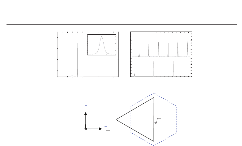
Figure 2 (a) shows the x-ray θ-2θ diffraction patterns of thick ZnO films on (111) STO
substrates. The diffractogram indicates only a single phase ZnO with a hexagonal wurtzite
structure. Only peaks of ZnO (0002) and (0004) reflection and no other ZnO related peaks are
observed, implying a complete c-axis oriented growth of the ZnO layer. The highly oriented
ZnO films on STO substrate strongly suggest that the nucleation and crystal growth is initiated
near the substrate surface. The full width at half maximum (FWHM) of symmetric (0002) scan
is about 0.85
◦
along ω-axis, as shown in the inset of Fig. 2(a). X-ray off-axis φ scans are
performed to identify the in-plane orientation relationships between the film and substrate.
The number of peaks in a φ scan corresponds to the number of planes for a particular family
that possesses the same angle with the film surface. Figure 2 (b) shows the results of x-ray
φ scans performed using the
{1122} reflection of ZnO (2θ=67.95
◦
, χ=58.03
◦
)andthe{110}
reflection of STO (2θ=32.4
◦
, χ=35.26
◦
). Only six peaks separated by 60
◦
are observed for the
ZnO
{112} family, which has six crystal planes with the same angle with the growth plane
(χ =58.03
◦
), as shown in Fig. 2 (b), indicating a single domain. From the relative position
of ZnO
{112} and STO {110} families, the in-plane relationships can be determined to be
[11
20]ZnO[011]STO. The atomic arrangement in the (0001) basal plane of ZnO is shown
in Fig. 2 (c). The growth in this direction shows a large lattice mismatch of about 17.7%
(
2a
ZnO
−
√
2a
STO
√
2a
STO
×100%) along the direction of <1120>
ZnO
, although it shows a much smaller
lattice mismatch of 1.91% (
√
3a
ZnO
−
√
2a
STO
√
2a
STO
×100%) along the direction of <1100>
ZnO
when
ZnO rotated 30
◦
in plane.
For ZnO/STO heterojunction, the VBO (ΔE
V
) can be calculated from the formula
ΔE
V
= ΔE
CL
+(E
ZnO
Zn2p
− E
ZnO
VBM
) − (E
STO
Ti2p
− E
STO
VBM
),(9)
310
Ferroelectrics - Characterization and Modeling
Valence Band Offsets of ZnO/SrTiO
3
, ZnO/BaTiO
3
,InN/SrTiO
3
, and InN/BaTiO
3
Heterojunctions Measured by X-ray Photoelectron Spectroscopy 7
20 30 40 50 60 70 80
-3 -2 -1 0 1 2 3
Intensity (arb. units.)
Z (deg.)
STO(111)
ZnO(004)
ZnO(002)
Intensity (arb. units.)
2T (deg.)
0 50 100 150 200 250 300 350
STO{110} (2T=32.40
o
F=35.26
o
)
ZnO{112} (2
T=67.95
o
F=58.03
o
)
Intensity (arb. units.)
I (deg.)
2 a
STO
a
ZnO
[1100]
[211
]
[011]
(111)STO
[112
0]
(0001)ZnO
(c)
(a) (b)
Fig. 2. X-ray θ-2θ (a), ω (inset of (a)), and φ (b) scans and atomic arrangement (c) of ZnO films
on (111) STO substrate.
where ΔE
CL
=(E
ZnO/STO
Ti2p
-E
ZnO/STO
Zn2p
) is the energy difference between Zn 2p and Ti 2p CLs
measured in the thin ZnO/STO heterojunction sample, and (E
STO
Ti2p
-E
STO
VBM
)and(E
ZnO
Zn2p
-E
ZnO
VBM
)
are the VBM energies with reference to the CL positions of bulk STO and thick ZnO film,
respectively, which are obtained by XPS measurement from the respective STO substrate and
thick ZnO film.
Figure 3 shows the XPS Ti 2p and Zn 2p CL narrow scans and the valence band spectra
from the STO substrate and the thick ZnO/STO samples, respectively. As shown in Fig.
3(a), the Zn 2p CL peak locates at 1021.69
±0.03 eV. Fig. 3(e) shows the VB spectra of the
thick ZnO sample, and the VBM position is determined to be 1.06
±0.06 eV by a linear fitting
depicted above. As a result, the energy difference of Zn 2p to ZnO VBM (E
ZnO
Zn2p
-E
ZnO
VBM
)can
be determined to be 1020.63
±0.03 eV. Using the same Voigt fitting and linear extrapolation
methods mentioned above, the energy difference of Ti2p to STO VBM (E
STO
Ti2p
-E
STO
VBM
)canbe
determined to be 457.32
±0.06 eV. The CL spectrum of Zn 2p and Ti 2p in thick ZnO film
and bulk STO are quite symmetric indicating the uniform bonding state and the only peaks
correspond to Zn-O and Ti-O bonds, respectively. The measurement of ΔE
CL
for the Ti 2p and
Zn 2p CLs recorded in the thin ZnO/STO junction is illustrated in Fig. 3(c) and (d). After
substraction of the background, the spectra of Ti 2p and Zn 2p CLs were well Voigt fitted and
the energy difference of Ti 2p and Zn 2p CLs (ΔE
CL
) can be determined to be 562.69±0.03
eV. It is noteworthy that the Ti 2p peak is not symmetric and consists of two components by
careful Voigt fitting. The prominent one located at 459.22 eV is attributed to the Ti emitters
within the STO substrate which have six bonds to oxygen atoms, and the other one shifting
by
∼2 eV to a lower binding energy indicates the presence of an interfacial oxide layer. This
phenomenon is similar to that observed in the interface of LaAlO
3
/SrTiO
3
, and the shoulder
at lower binding energy is attributed to TiO
x
suboxides, which is expected on account of the
TiO
x
-terminated STO initial surface (Kazzi et al., 2006). The fair double-peak fitting shown
311
Valence Band Offsets of ZnO/SrTiO
3
, ZnO/BaTiO
3
,
InN/SrTiO
3
, and InN/BaTiO
3
Heterojunctions Measured by X-Ray Photoelectron Spectroscopy

8 Will-be-set-by-IN-TECH
in Fig. 3(d) confirms the presence of TiO
x
suboxides. Substituting the above (E
STO
Ti2p
-E
STO
VBM
),
(E
ZnO
Zn2p
-E
ZnO
VBM
)andΔE
CL
into Eq. 9, the resulting VBO value is calculated to be 0.62±0.09 eV.
1010 1015 1020 1025 1030
(a) ZnO: Zn2p
1021.69 eV
-4 -2 0 2 4 6
1.06 eV
(e) ZnO: VBM
-4-202468
0.98 eV
(f) STO: VBM
445 450 455 460 465 470
(b) STO: Ti2p
458.30 eV
1010 1015 1020 1025 1030
(c) ZnO/STO: Zn2p
1021.91 eV
445 450 455 460 465 470
(d) ZnO/STO: Ti2p
459.22 eV
Binding energy (eV)
Intensit
y(
arb. units
)
Fig. 3. Zn 2p spectra recorded on ZnO (a) and ZnO/STO (c), Ti 2p spectra on STO (b) and
ZnO/STO (d), and VB spectra for ZnO (e) and STO (f). All peaks have been fitted to Voigt
line shapes using Shirley background, and the VBM values are determined by linear
extrapolation of the leading edge to the base line. The errors in the peak positions and VBM
are
±0.03 and ±0.06 eV, respectively.
The reliability of the measured result is analyzed by considering several possible factors that
could impact the experiment results. The lattice mismatch between ZnO and STO is about
∼17.7%, which will induce a much smaller critical thickness than 5-10 nm, compared with
the lattice mismatch of BaTiO
3
grown on STO (2.2%) and a critical thickness of 5-10 nm
(Sun et al., 2004). Meanwhile, the ZnO epitaxial layer grown on STO substrate by MOCVD is
characterized by columnar growth mode, which provides strain relief mechanism (Fan et al.,
2008). Thus, the ZnO overlayer in the heterojunction is almost completely strained and the
strain-induced piezoelectric field effect can also be neglected. In addition, the error induced
by band bending is checked to be much smaller than the average standard deviation of
±0.09
eV given above (Yang et al., 2009). Since the factors that can affect the ultimate result can be
excluded from the measured result, the experimental obtained VBO value is reliable.
To further confirm our result, it would be very useful to compare our experimental results
with a theoretical model proposed by M
¨
onch (Monch et al., 2005). The VBOs of ZnO
heterojunctions are predicted based on the difference of the respective interface-induced gap
312
Ferroelectrics - Characterization and Modeling

Valence Band Offsets of ZnO/SrTiO
3
, ZnO/BaTiO
3
,InN/SrTiO
3
, and InN/BaTiO
3
Heterojunctions Measured by X-ray Photoelectron Spectroscopy 9
states (IFIGS) branch-point energies and electric dipole terms. That is
ΔE
V
= E
vl
(Γ) − E
vr
(Γ)=φ
p
bpr
−φ
p
bpl
+ D
X
(X
sr
− X
sl
), (10)
where the p-type branch-point energy φ
p
bp
(Γ)=E
bp
− E
V
(Γ) is the energy distance from the
valence band maximum to the branch point of the IFIGS and X
s
is the electronegativity of the
respective semiconductor. The subscripts r and l stand for the right and left side, respectively,
of the heterostructure. The dipole parameter D
X
is determined by the density of states and
extension of the IFIGS at their branch point. This dipole term can also be neglected, just
like the common semiconductor heterojunctions, since the electronegativities of the atoms
constituting ZnO/STO heterojunction differ by up to 10% only. Through analysis of the VBO
values reported for ZnO heterostructure (Monch et al., 2005), the dependence of VBO on the
p-type branch-point energy is obtained to be
ΔE
V
= ϕ
vbo
[φ
p
bp
(ZnO) − φ
p
bp
(semi)]. (11)
With the p-type branch-point energies of ZnO (3.04 eV) (Monch et al., 2005) and STO (2.5
eV) (Monch et al., 2004), and the slope parameters ϕ
vbo
for insulator heterostructures of
1.14
∼1.23, a VBO of 0.64±0.21 eV would be calculated, which is in good agreement with
the experimentally determined value of 0.62
±0.09 eV. It implies that the IFIGS theory is not
only widely used to the group-IV elemental semiconductors, SiC, and the III-V, II-VI, and
I-III-VI
2
compound semiconductors and their alloys (Monch et al., 2005), but also applicable to
the semiconductor/insulator heterostructures. In addition, the resulting ΔE
V
is a sufficiently
large value for device applications in which strong carrier confinement is needed, such as
light emitters or heterostructure field effect transistors. For instance, the valence band offset
in the Zn
0.95
Cd
0.05
O/ZnO system is only 0.17 eV (Chen et al., 2005), which is less than that of
ZnO/STO.
Finally, the CBO (ΔE
C
) can be estimated by the formula ΔE
C
=ΔE
V
+E
ZnO
g
-E
STO
g
.By
substituting the band gap values (E
ZnO
g
=3.37 eV (Su et al., 2008) and E
STO
g
=3.2 eV (Baer et al.,
1967)), ΔE
C
is calculated to be 0.79±0.09 eV. It would be interesting to compare
our experimental values with the electrical transport results by Wu et al (Wu et al.,
2008). They have investigated the temperature dependent current-voltage characteristic of
ZnO/Nb:SrTiO
3
junction, and found that the effective barrier height (φ
eff
)is0.73eV,which
is directly considered to be the CBO in n-N heterojunctions (Alivov et al., 2006). It can be seen
that the effective barrier height in Wu’s work is consistent with our CBO value. Accordingly,
a type-II band alignment forms at the heterojunction interface, in which the conduction and
valence bands of the ZnO film are concomitantly higher than those of the STO substrate, as
shown in Fig. 4.
5. VBO for ZnO/BTO heterojunction
In x-ray θ-2θ diffraction measurements, as shown in Fig. 5 (a), the ZnO/BTO sample presented
the only peak of ZnO (0002) reflection and no other ZnO related peaks were observed,
implying a complete c-axis oriented growth of the ZnO layer. From the pole figure of ZnO
{1011} family, shown in Fig. 5 (b), twelve peaks separated by 30
◦
are present, although ZnO
has a sixfold symmetry about the [0001] axis, indicating that the ZnO film is twinned in the
growth plane by a 30
◦
in-plane rotation. The relative intensities of the two sets of peaks is
313
Valence Band Offsets of ZnO/SrTiO
3
, ZnO/BaTiO
3
,
InN/SrTiO
3
, and InN/BaTiO
3
Heterojunctions Measured by X-Ray Photoelectron Spectroscopy

10 Will-be-set-by-IN-TECH
STO ZnO
E
Ti2p
STO
E
c
ZnO
E
v
ZnO
E
Zn2p
ZnO
E
c
STO
E
v
STO
E
g
STO
=3.2 eV
E
g
ZnO
=3.37 eV
(E
Zn2p
-E
v
)
ZnO
=1020.63 eV
(E
Ti2p
-E
v
)
STO
=457.32 eV
ǻE
c
=0.79 eV
ǻE
v
=0.62 eV
ǻE
CL
=562.69 eV
Fig. 4. Energy band diagram of ZnO/STO heterojunction.
related to the proportion of the two domains, indicating that the two domains are almost
equal in amount.
10 20 30 40 50 60 70 80
BTO (200)
BTO (002)
BTO (100)
BTO (001)
ZnO (002)
Intensity (arb. units.)
2T (deg.)
(a) (b)
Fig. 5. X-ray θ-2θ diffraction pattern (a) and pole figure (b) of the thick ZnO films on BTO
substrates.
For ZnO/BTO heterojunction, the VBO (ΔE
V
) can be calculated from the formula
ΔE
V
= ΔE
CL
+(E
ZnO
Zn2p
− E
ZnO
VBM
) −(E
BTO
Ti2p
− E
BTO
VBM
), (12)
where ΔE
CL
=(E
ZnO/BTO
Ti2p
-E
ZnO/BTO
Zn2p
) is the energy difference between Zn 2p and Ti 2p CLs
measured in the thin ZnO/BTO heterojunction, while (E
BTO
Ti2p
-E
BTO
VBM
)and(E
ZnO
Zn2p
-E
ZnO
VBM
)arethe
VBM energies with reference to the CL positions of bulk BTO and thick ZnO film, respectively.
Figure 6 shows the XPS T i 2p and Zn 2p CL narrow scans and the valence band spectra from
the bulk BTO, thick and thin ZnO/BTO samples, respectively. For the thick ZnO film, the Zn
2p CL peak locates at 1022.04
±0.03 eV, and the VBM position is determined to be 2.44±0.06
eV by a linear fitting described above, as shown in Fig. 6(a) and (e). The energy difference
between Zn 2p and VBM of thick ZnO film (E
ZnO
Zn2p3
-E
ZnO
VBM
) is deduced to be 1019.60±0.09
eV, which is well consistent with our previous reports (Zhang et al., 2007). It can also be
clearly seen from Fig. 6 that the CL spectra of Zn 2p and Ti 2p in the thick ZnO film and
thin ZnO/BTO heterojunction are quite symmetric, indicating a uniform bonding state and
314
Ferroelectrics - Characterization and Modeling

Valence Band Offsets of ZnO/SrTiO
3
, ZnO/BaTiO
3
,InN/SrTiO
3
, and InN/BaTiO
3
Heterojunctions Measured by X-ray Photoelectron Spectroscopy 11
-202468
2.44 eV
(e) ZnO: VBM
-202468
1.49 eV
(f) BTO: VBM
455 460 465
457.12 eV
(b) BTO: Ti 2p
1015102010251030
(a) ZnO: Zn 2p
1022.04 eV
1015102010251030
(c) ZnO/BTO: Zn 2p
1021.17 eV
455 460 465
457.68 eV
(d) ZnO/BTO: Ti 2p
Binding energy (eV)
Intensity (arb. units)
Fig. 6. Zn 2p spectra recorded on ZnO (a) and ZnO/BTO (c), Ti 2p spectra on BTO (b) and
ZnO/BTO (d), and VB spectra for ZnO (e) and BTO (f). All peaks have been fitted to Voigt
line shapes using Shirley background, and the VBM values are determined by linear
extrapolation of the leading edge to the base line. The errors in the peak positions and VBM
are
±0.03 and ±0.06 eV, respectively.
BTO ZnO
E
Ti2p
BTO
E
c
ZnO
E
v
ZnO
E
Zn2p
ZnO
E
c
BTO
E
v
BTO
E
g
BTO
=3.1 eV
E
g
ZnO
=3.37 eV
(E
Zn2p
-E
v
)
ZnO
=1019.60 eV
(E
Ti2p
-E
v
)
BTO
=455.63 eV
ǻE
c
=0.75 eV
ǻE
v
=0.48 eV
ǻE
CL
=563.49 eV
Fig. 7. Energy band diagram of ZnO/BTO heterojunction.
the only peaks correspond to Zn-O and Ti-O bonds, respectively. However, the Ti 2p peak
in the bulk BTO is not symmetric and consists of two components by careful Voigt fitting.
The prominent one located at 457.12
±0.03 eV is attributed to the Ti emitters within the BTO
substrate, which have six bonds to oxygen atoms. The other one shifting by
∼2eVtoalower
315
Valence Band Offsets of ZnO/SrTiO
3
, ZnO/BaTiO
3
,
InN/SrTiO
3
, and InN/BaTiO
3
Heterojunctions Measured by X-Ray Photoelectron Spectroscopy

12 Will-be-set-by-IN-TECH
binding energy is attributed to TiO
x
suboxides on account of the TiO-terminated BTO initial
surface (Kazzi et al., 2006). It is interesting that the Ti 2p peaks transform from asymmetry
in bulk BTO to symmetry in the thin ZnO/BTO sample, implying that the TiO
x
suboxides
in the BTO surface is oxidized completely to the highest valence of Ti
4+
.TheVBMvalueof
bulk BTO is determined to be 1.49
±0.06 eV using the linear method. The Fermi level of an
insulator is expected to be located in the middle of the forbidden energy gap, so the VBM
will be one-half of the band gap of insulators (You et al., 2009). For BTO, the VBM should
be 1.55 eV calculated from the band gap of 3.1 eV (Boggess et al., 1990), which is in good
agreement with the measured value (1.49
±0.06 eV) in the present work. Using the same fitting
methods mentioned above, the energy values of CL for the thin ZnO/BTO heterojunction can
be determined, as shown in Fig. 6. Substituting the above values into Eq. 12, the resulting
VBO value is calculated to be 0.48
±0.09 eV.
A small lattice mismatch is present between the BTO[0
11] direction and the hexagonal
apothem of ZnO, which is only about 0.8% (
√
3a
ZnO
−
√
2a
BTO
√
2a
BTO
×100%) (Wei et al., 2007). This
lattice mismatch is so small that the strain-induced piezoelectric field effect can be neglected
in this work (Su et al., 2008). In ZnO/MgO heterostructure, the 8.3% mismatch brings a shift
of 0.22 eV on VBO (Li et al., 2008). By linear extrapolation method, the strain induced shift in
ZnO/BTO is less than 0.02 eV, which is much smaller than the aforementioned deviation of
0.09 eV. The error induced by band bending is checked to be much smaller than the average
standard deviation of 0.09 eV given above (Yang et al., 2009). So the experimental obtained
VBO value is reliable.
To further confirm the reliability of the experimental values, it would be useful to compare
our VBO value with other results deduced by transitive property. For heterojunctions formed
between all pairs of three materials (A, B, and C), ΔE
V
(A-C) can be deduced from the
difference between ΔE
V
(A-B) and ΔE
V
(C-B) neglecting the interface effects (Foulon et al.,
1992). The reported VBO values for some heterojunctions are ΔE
V
(ZnO-STO)=0.62 eV
(Jia et al., 2009b), ΔE
V
(Si-STO)=2.38 or 2.64 eV, and ΔE
V
(Si-BTO)=2.35 or 2.66 eV (Amy et al.,
2004), respectively. Then the ΔE
V
(ZnO-BTO) is deduced to be 0.59, 0.64, 0.9 or 0.33 eV, which
is comparable to our measured value 0.48
±0.09 eV. Since the samples were prepared under
different growth conditions, the different interfaces are responsible for the difference between
our measured value and the results from the transitivity. In addition, the resulting ΔE
V
is a
sufficiently large value for device applications which require strong carrier confinement, such
as light emitters or heterostructure field effect transistors (Chen et al., 2005).
Finally, the CBO (ΔE
C
) can be estimated by the formula ΔE
C
=ΔE
V
+E
ZnO
g
-E
BTO
g
.By
substituting the band gap values at room temperature (E
ZnO
g
=3.37 eV (Su et al., 2008) and
E
BTO
g
=3.1 eV (Boggess et al., 1990)), ΔE
C
is calculated to be 0.75±0.09 eV. Accordingly, a type-II
band alignment forms at the heterojunction interface, in which the conduction and valence
bands of the ZnO film are concomitantly higher than those of the BTO substrate, as shown in
Fig. 7.
6. VBO for InN/STO heterojunction
Figure 8 (a) shows the typical XRD θ-2 θ patterns of InN thin films deposited on (001) STO
substrates. InN crystals shows an intense diffraction line at 2θ=31.28
◦
assigned to the (0002)
diffraction of InN with hexagonal wurtzite structure, implying that the c-axis of InN films
is perpendicular to the substrate surface. Figure 8 (b) shows the results of x-ray off-axis
316
Ferroelectrics - Characterization and Modeling

Valence Band Offsets of ZnO/SrTiO
3
, ZnO/BaTiO
3
,InN/SrTiO
3
, and InN/BaTiO
3
Heterojunctions Measured by X-ray Photoelectron Spectroscopy 13
φ scans performed using the {1011} reflection of InN (2θ=33.49
◦
, χ=61.86
◦
)andthe{111}
reflection of STO (2θ=39.96
◦
, χ=54.74
◦
) to determine the in-plane orientation of the InN film
relative to STO. Although InN has a sixfold symmetry about the [0001] axis, the presence of
twelve peaks separated by 30
◦
for {1122} reflections indicates that the InN films is twinned
in the growth plane by a 30
◦
in-plane rotation. The relative intensities of the two sets of
peaks is related to the proportion of the two domains, indicating almost the same amount
for the two domains. Comparing the locations in φ-space of the InN{10
11} with STO{111}
families, the two-dimensional epitaxial relationships for the two domains can be derived to
be [1
100]InN[110]STO for one domain and [1120]InN[110]STO for the other. The atomic
arrangements for the two domains are illustrated in the schematic drawings of Fig. 8(c).
20 30 40 50 60 70 80
InN(112)
InN(004)
STO(003)
STO(002)
Intensity (arb. units.)
2T (deg.)
InN(002)
STO(001)
K
E
-150 -100 -50 0 50 100 150
STO{111} (2T=39.96
o
, F=54.74
o
)
InN{101} (2
T=33.49
o
, F=61.86
o
)
I(deg.)
(b)(a)
a
STO
a
InN
a
InN
(c)
Fig. 8. X-ray θ-2θ (a) and φ (b) scanning patterns, and atomic arrangement (c) of the thick InN
films on (001)STO substrates.
For InN/STO heterojunction, the VBO (ΔE
V
) can be calculated from the formula
ΔE
V
= ΔE
CL
+(E
InN
In3d
− E
InN
VBM
) −(E
STO
Ti2p
− E
STO
VBM
), (13)
where ΔE
CL
=(E
InN/STO
Ti2p
-E
InN/STO
In3d
) is the energy difference between In 3d and Ti 2p CLs
measured in the thin InN/STO heterojunction, while (E
STO
Ti2p
-E
STO
VBM
)and(E
InN
In3d
-E
InN
VBM
)arethe
VBM energies with reference to the CL positions of bulk STO and thick InN film, respectively.
Fig. 9 shows In 3d, Ti 2p CL narrow scans and valence band spectra recorded on thick InN,
bulk STO and thin InN/STO heterojunction samples, respectively. The In 3d spectra in thick
InN films include two peaks of 3d
5/2
(443.50±0.03 eV) and 3d
3/2
(451.09±0.03 eV), which
are separated by the spin-orbit interaction with a splitting energy of around 7.57 eV. Both
peaks are found out to consist of two components by careful Voigt fitting. The first In 3d
5/2
component located at 443.50±0.03 eV is attributed to the In-N bonding, and the second, at
444.52
±0.03 eV, is identified to be due to surface contamination. This two-peak profile of the
In 3d
5/2
spectra in InN is typical and have been demonstrated by other researchers (King et al.,
2008; Piper et al., 2005; Yang et al., 2009). Comparison of their binding energy separation with
previous results, we suggest that the second peak at 444.52
±0.03 eV to the In-O bonding is due
to contamination by oxygen during the growth process. The ratio of In-N peak intensity to
317
Valence Band Offsets of ZnO/SrTiO
3
, ZnO/BaTiO
3
,
InN/SrTiO
3
, and InN/BaTiO
3
Heterojunctions Measured by X-Ray Photoelectron Spectroscopy
14 Will-be-set-by-IN-TECH
-2 0 2 4 6 8
0.45 eV
(e) InN: VBM
-20246810
(f) STO: VBM
1.91 eV
440 445 450 455
(a) InN: In3d
443.50 eV
455 460 465
(b) STO: Ti 2p
458.32 eV
440 445 450 455
(c) InN/STO: In 3d
443.68 eV
455 460 465
(d) InN/STO: Ti 2p
458.17 eV
Binding energy (eV)
Intensit
y(
arb. units
)
Fig. 9. In 3d spectra recorded on InN (a) and InN/STO (c), Ti 2p spectra on STO (b) and
InN/STO (d), and VB spectra for InN (e) and STO (f). All peaks have been fitted to Voigt line
shapes using Shirley background, and the VBM values are determined by linear
extrapolation of the leading edge to the base line. The errors in the peak positions and VBM
are
±0.03 and ±0.06 eV, respectively.
STO
InN
E
Ti2p
STO
E
c
InN
E
v
InN
E
In3d
InN
E
c
STO
E
v
STO
E
g
STO
=3.2 eV
E
g
InN
=0.7 eV
(E
In3d
-E
v
)
InN
=443.05 eV
(E
Ti2p
-E
v
)
STO
=456.41 eV
ǻE
c
=1.37 eV
ǻE
v
=1.13 eV
ǻE
CL
=14.49 eV
Fig. 10. Energy band diagram of InN/STO heterojunction.
the oxygen related peaks indicates that only a small quantity of oxygen contamination exists
in our samples. Both the Ti 2p spectra in bulk STO and thin InN/STO heterojunction are
quite symmetric, indicating a uniform bonding state. Using the linear extrapolation method
mentioned above, the VBM of InN and STO are 0.45
±0.06 eV and 1.91±0.06 eV respectively.
318
Ferroelectrics - Characterization and Modeling