Lallart M. Ferroelectrics: Characterization and Modeling
Подождите немного. Документ загружается.

12
Changes of Crystal Structure
and Electrical Properties with Film
Thickness and Zr/(Zr+Ti) Ratio for
Epitaxial Pb(Zr,Ti)O
3
Films Grown on
(100)
c
SrRuO
3
//(100)SrTiO
3
Substrates by
Metalorganic Chemical Vapor Deposition
Mohamed-Tahar Chentir
1
, Hitoshi Morioka
1,2
,
Yoshitaka Ehara
1
, Keisuke Saito
2
, Shintaro Yokoyama
1
,
Takahiro Oikawa
1
and Hiroshi Funakubo
1
1
Tokyo Institute of Technology, Department of Innovative and Engineered Materials,
Interdisciplinary Graduate School of Science and Engineering
2
Application Laboratory, Bruker AXS
Japan
1. Introduction
Lead zirconium titanate, Pb(Zr,Ti)O
3
[PZT], have been intensively studied for various
ferroelectric applications, and have a renewal interest due to their promising application for
microelectromechanical systems (MEMS) because of their outstanding ferroelectric and
piezoelectric properties. Remanent polarization (P
r
) is the not only most fundamental
parameter but also the practical importance for real applications to achieve high density
devices. Spontaneous polarization (P
S
) is the expected maximum P
r
value of the materials
that depend on the composition, orientation and the crystallinity of Pb(Zr,Ti)O
3
. Thus, in an
academic point of view, lots of efforts have been made to investigate P
S
value. However,
PZT crystals with single domain are hard to be obtained, inducing a lack of direct
characterization of P
S
values using PZT single crystal. This situation is due to c/a/c/a
polydomain structure of PZT, where a domain and c domain are respective (100) and (001)
oriented domains. This domain structure is the result of relaxation process of stress induced
under the growth process of PZT.
To achieve this purpose, we switch our idea from growth of the bulky single crystal to
epitaxial films with polar axis orientation. In addition, a comprehensive and systematic
characterization of ferroelectric properties of PZT films with different volume fraction of
polar-axis-oriented domain is investigated.
This chapter investigates the thickness and Zr/(Zr+Ti) ratio dependencies of domain
structure and ferroelectric properties, and correlates physical properties, namely lattice

Ferroelectrics - Characterization and Modeling
230
parameters and the volume fractions of the domains, as well as the electrical properties such
as P
r
and P
S
.
2. Experimental
PZT thin films were grown on (100)
c
SrRuO
3
//(100)SrTiO
3
substrates at 540ºC by pulsed-
metal organic chemical vapor deposition (MOCVD) from Pb(C
11
H
19
O
2
)
2
- Zr(O·t-C
4
H
9
)
4
-
Ti(O·i-C
3
H
7
)
4
- O
2
system (Nagashima et al., 2001). Epitaxial (100)
c
SrRuO
3
thin films used for
bottom electrode layers were grown on (100)SrTiO
3
substrates by MOCVD (Okuda et al.,
2000). The Zr/(Zr+Ti) ratio and the film thickness of PZT films were controlled by the input
gas concentration of the source gases and the deposition time, respectively. In this work, we
studied PZT films having thickness ranging from 50 to 250 nm.
The orientation of the deposited films was analyzed by high-resolution X-Ray Diffraction
(XRD) using a four-axis diffractometer (PANalytical X’Pert MRD). The high-resolution
XRD reciprocal space mapping (HRXRD-RSM) was also employed for more detail
analysis of crystal structure (orientation, in-plane and out-of-plane lattice parameters, and
the internal axial angle) and estimating the relative volume fraction of the c-domain in
tetragonal phase (Saito et al., 2003a).
Electron-beam deposition was used to deposit 100 μm
φ
Pt top electrodes for the electrical
property characterization of PZT films. The polarization – electric-field (P - E) hysteresis
loops of the as-deposited films were measured at 20 Hz by the ferroelectric tester using
pulsed rectangular wave (Radiant Technologies RT6000HVS and TOYO Corporation
FCE-1).
3. Results and discussion
In this section, we demonstrate, first of all, film thickness dependency of the crystal
structure of PZT films. We show that polar-axis-oriented films were obtained at very thin
films region. Then, we detail the Zr/(Zr+Ti) ratio dependency of the domain structure. For
this purpose, we will compare crystal structure evolution as a function of the Zr/(Zr+Ti)
ratio at two thicknesses, 50 and 250 nm. This comparative study aims to emphasis the role of
the Zr/(Zr+Ti) ratio in PZT film as well as the thickness dependency, discussed in first
instance.
Finally, we will cross check the up mentioned results by monitoring the evolution of
electrical properties versus thickness and the Zr/(Zr+Ti) ratio in the films. We will synthesis
these data by identifying the linear relationship between the square of spontaneous
polarization (P
s
2
) and tetragonal distortion (1-c/a).
Nevertheless, prior to proceeding to this characterization, it is important to check the
epitaxial relationship between the bottom electrode and PZT films.
Indeed, it must be kept in mind that the framework of this study is the fundamental
understanding of the impact of crystal structure change on the electrical properties, and
polycrystalline films might induce measurement artefacts. The epitaxial growth of PZT films
on (100)SrRuO
3
//(100)SrTiO
3
substrates was ascertained by High Resolution Transmittance
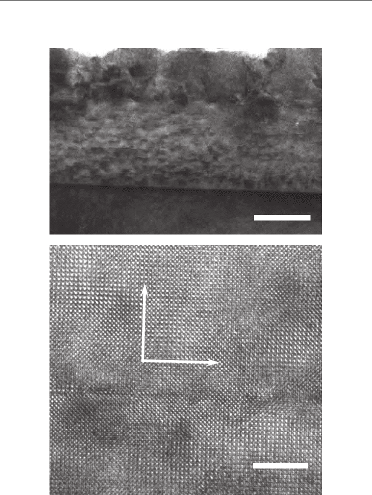
Electron Microscopy (HRTEM) as presented on Fig. 1(a).
Indeed, Fig. 1(a) shows a cross-sectional TEM image of 50 nm thick PZT(35/65) film. It
presents smooth interfaces. Fig. 1(b) reveals atomically sharp interface between PZT and
Changes of Crystal Structure and Electrical Properties with Film Thickness and
Zr/(Zr+Ti) Ratio for Epitaxial Pb(Zr,Ti)O
3
films Grown on (100)
c
SrRuO
3
//(100)SrTiO
3
Substrates…
231
SrRuO
3
bottom electrode. Moreover, this latter figure shows clearly a coherent epitaxial
relationship at PZT/SrRuO
3
interface.
SrRuO
3
PZT
5nm
50nm
SrRuO
3
PZT
SrTiO
3
(a)
(b)
[001]PZT
<100>PZT
Fig. 1. Cross sectional TEM imaging of PZT(35/65)/SrRuO
3
/SrTiO
3
(a). HRTEM of
PZT-SrRuO
3
interface reveals a coherent epitaxial growth of PZT on SrRuO
3
bottom
electrode (b).
Ferroelectrics - Characterization and Modeling
232
3.1 Evolution of domain structure versus film thickness
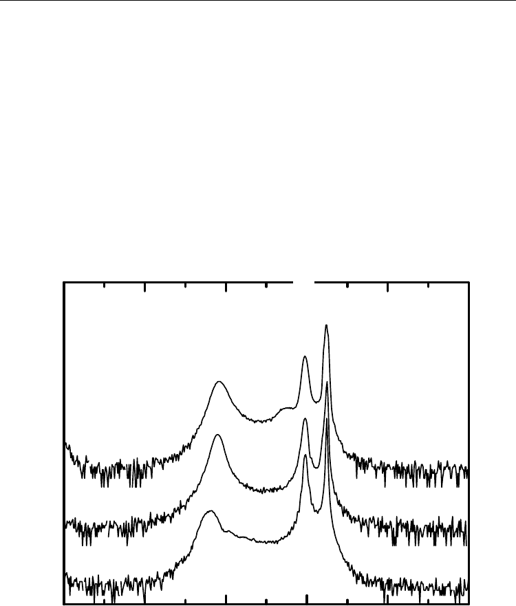
For this part of our investigation, we chose to characterize PZT films with the Zr/(Zr+Ti)
ratio of 0.35 that have a tetragonal symmetry. Fig. 2 presents XRD plots for the 2
θ
angle
range of 2θ = 40 - 50°. On this figure we notice that PZT 200 peak decreases with
decreasingly film thickness. This phenomenon might have two possibilities: one is the
change of the tilting angle against the surface normal direction. The other is the change of
domain structure from the mixed domain structure of a and c domains to fully c-domain
oriented film with decreasing film thickness.
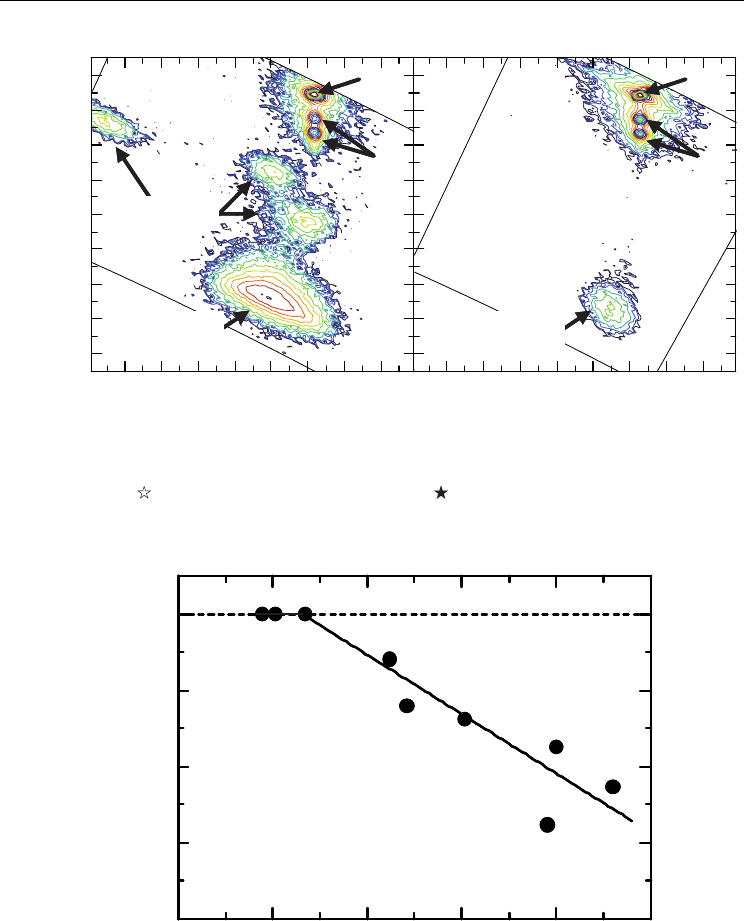
Hence, using XRD-RSM technique (Fig. 3), we could monitor c-domain volume fraction
[V
c
=V
(001)
/(V
(100)
+V
(001)
)] as a function of film thickness as shown in Fig. 4. On this figure, we
notice that films having thicknesses under around 75 nm, are perfect polar axis-oriented
films. Over this threshold, c-domain volume fraction decreases almost linearly with
increasing thickness up to 230 nm..
40 42 44 46 48 50
002
200
SrRuO
3
200
c
SrTiO
3
200
50nm
110nm
Thickness;
200nm
Log [intensity (arb. units)]
Pt 111
[Top electrodes]
2
θ
, CuKα
1
(deg)
Fig. 2. XRD plots of PZT(35/65) films having thicknesses ranging from 50 to 200 nm. As
film thickness increases, PZT 200 peak appears indicating the coexistence of a-domain with
c-domains.
Changes of Crystal Structure and Electrical Properties with Film Thickness and
Zr/(Zr+Ti) Ratio for Epitaxial Pb(Zr,Ti)O
3
films Grown on (100)
c
SrRuO
3
//(100)SrTiO
3
Substrates…
233
4.6 4.7 4.8 4.9 5.0 5.1 5.2 5.3
9.5
9.6
9.7
9.8
9.9
10
10.1
10.2
10.3
q
x
//SrTiO
3
[100] (nm
-1
)
q
z
//SrTiO
3
[001] (nm
-1
)
4.6 4.7 4.8 4.9 5.0 5.1 5.2 5.3
q
x
//SrTiO
3
[100] (nm
-1
)
☆☆
★★
PZT 204PZT 204
PZT 402
4.6 4.7 4.8 4.9 5.0 5.1 5.2 5.3
9.5
9.6
9.7
9.8
9.9
10
10.1
10.2
10.3
q
x
//SrTiO
3
[100] (nm
-1
)
q
z
//SrTiO
3
[001] (nm
-1
)
4.6 4.7 4.8 4.9 5.0 5.1 5.2 5.3
q
x
//SrTiO
3
[100] (nm
-1
)
☆☆
★★
PZT 204PZT 204
PZT 402
4.6 4.7 4.8 4.9 5.0 5.1 5.2 5.3
9.5
9.6
9.7
9.8
9.9
10
10.1
10.2
10.3
q
x
//SrTiO
3
[100] (nm
-1
)
q
z
//SrTiO
3
[001] (nm
-1
)
4.6 4.7 4.8 4.9 5.0 5.1 5.2 5.3
q
x
//SrTiO
3
[100] (nm
-1
)
☆☆
★★
PZT 204PZT 204
PZT 402
(a) (b)
Fig. 3. XRD-RSM of PZT(35/65) films having thicknesses of (a) 250 nm and (b) 50 nm.
SrTiO
3
204 spot ( ) and splitted sport of SrRuO
3
204 (
) are also illustrated.
0 50 100 150 200 250
0.6
0.7
0.8
0.9
1.0
Film thickness (nm)
V
(001)
/ [V
(100)
+V
(001)
]
0 50 100 150 200 250
0.6
0.7
0.8
0.9
1.0
Film thickness (nm)
V
(001)
/ [V
(100)
+V
(001)
]
Fig. 4. Evolution of c-domain volume fraction [V
c
=V
(001)
/(V
(100)
+V
(001)
)] as a function of PZT
thickness in the case of PZT(35/65) films.
Ferroelectrics - Characterization and Modeling
234
Finally, we checked strain condition when film thickness decrease in the case of PZT(35/65)
material. For this purpose, we calculated the both in-plan (a
//
and c
//
) and out-of-plan
(
a
⊥
and
c
⊥
) lattice parameters as a function of PZT film thickness (Fig. 5). On this figure, we
also indicate SrTiO
3
lattice parameter (a= 0.3905 nm) as well as unstrained PZT(35/65) lattice
parameters extracted from powder data (a = 0.398 nm and c = 0.413 nm) (Shirane & Suzuki,
1952). It is interesting to notice that in-plan and out-of-plan lattice parameters are almost
constant regardless of the film thickness range studied in this work, demonstrating almost
relaxed unit cells due to the large lattice mismatch between Pb(Zr
0.35
Ti
0.65
)O
3
films and SrTiO
3
substrates.
0 50 100 150 200 250
0.39
0.40
0.41
0.42
Film thickness (nm)
Lattice parameter (nm)
c
⊥
a
⊥
a
//
c
//
SrTiO
3
0 50 100 150 200 250
0.39
0.40
0.41
0.42
Film thickness (nm)
Lattice parameter (nm)
c
⊥
a
⊥
a
//
c
//
SrTiO
3
Fig. 5. In-plane and out-of-plane lattice parameters as function of film thickness in the case
of Pb(Zr
0.35
Ti
0.65
)O
3
films.
3.2 Domain structure evolution versus film composition
Fig. 6 presents X-ray diffraction diagrams of PZT films having 50 and 250 nm in thickness with
various Zr/(Zr+Ti) ratio. All films are found to have (100) and/or (001) orientations regardless
of the film thickness and Zr/(Zr+Ti) ratio. Epitaxial relationship of (001)/(100)PZT
//(100)
c
SrRuO
3
//(100) SrTiO
3
was ascertained by XRD pole figure measurement for all films.
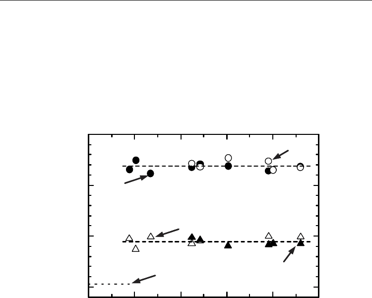
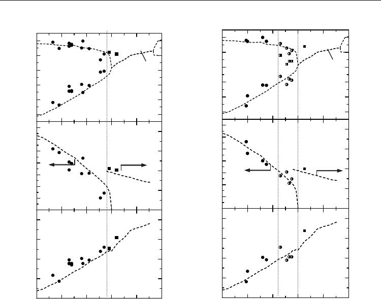
Figures 7(a) - (f) summarize a- and c-axes lattice parameters, tetragonality (c/a ratio) and the
internal angles (α), and the unit cell volume as a function of the Zr/(Zr+Ti) ratio for 50 and
250 nm-thick PZT films. Reported data by Shirane et al. for PZT powder are also presented
on these figures (Shirane & Suzuki, 1952).
As shown in Fig. 7, our experimental data are in good agreement with reported data of
powders. However, an intermediate region can easily be observed in the 250 nm thick
sample. This region could be related to the coexistence of both tetragonal and rhombohedral
phases (Morioka et al. 2004a), suggesting a strain relaxation mechanism at this thickness
(Morioka et al. 2004b).
Changes of Crystal Structure and Electrical Properties with Film Thickness and
Zr/(Zr+Ti) Ratio for Epitaxial Pb(Zr,Ti)O
3
films Grown on (100)
c
SrRuO
3
//(100)SrTiO
3
Substrates…
235
001 , 100
002
200
SrRuO
3
100
c
SrTiO
3
100
SrRuO
3
200
c
SrTiO
3
200
Pt 111
[Top electrodes]
100
200
Log [intensity (arb. units)]
20 30 40 50
2
θ
, CuKα
1
(deg)
(a)
(b)
(c)
(d)
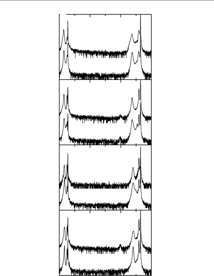
0.19
Zr/(Zr+Ti) ; 0.13
0. 30
0. 35
0. 54
0. 53
0. 67
0. 63
250nm
50nm
250nm
50nm
250nm
50nm
250nm
50nm
Fig. 6. XRD ω-2θ diagrams of PZT films having 50 and 250 nm in thickness and different
Zr/(Zr+Ti) ratio: from small Zr/(Zr+Ti) ratio (a) to large Zr/(Zr+Ti) ratio (d).
Ferroelectrics - Characterization and Modeling
236
0.390
0.395
0.400
0.405
0.410
0.415
Lattice parameter (nm)
Shirane et al.
1.00
1.01
1.02
1.03
1.04
1.05
1.06
1.07
0.0
0.1
0.2
0.3
0.4
c/a ratio
90–
α
(°)
0.0 0.2 0.4 0.6 0.8 1.0
62
64
66
68
70
Unit cell volume (10
-3
nm
3
)
Zr/(Zr+Ti) ratio
0.390
0.395
0.400
0.405
0.410
0.415
Shirane et al.
Lattice parameter (nm)
1.00
1.01
1.02
1.03
1.04
1.05
1.06
1.07
0.0
0.1
0.2
0.3
0.4
c/a ratio
90–
α
(°)
0.0 0.2 0.4 0.6 0.8 1.0
62
64
66
68
70
Zr/(Zr+Ti) ratio
Unit cell volume (10
-3
nm
3
)
(a)
(b)
(c)
(d)
(e)
(f)
Thickness : 50nm
Thickness : 250nm
Fig. 7. Lattice parameters (a, d), tetragonality, c/a ratio, and the internal angles and (b, e), and
unit cell volume (c, f) as a function of Zr/(Zr+Ti) ratio for (a)-(c) 50 and (d)-(f) 250 nm thick
films. Dashed lines are powder data reported by Shirane et al (Shirane & Suzuki, 1952).
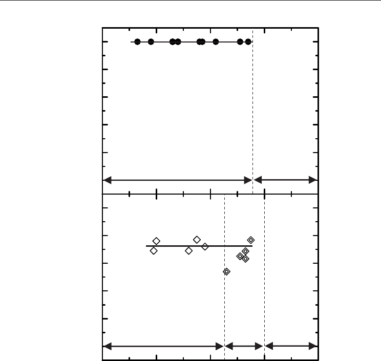
The c-domain relative volume fractions, V
c
, are shown in Fig. 8 as a function of the
Zr/(Zr+Ti) ratio. These values are obtained from HRXRD-RSM characterization reported
elsewhere (Morioka et al. 2004a).
On this figure we notice that the 50 nm thick Films are fully polar axis-oriented films, (001)
orientation, regardless of the Zr/(Zr+Ti) ratio up to 54% (Fig. 8(a)). On the other hand, V
c
decreased with increasing PZT film thickness. Indeed, we notice for the 250 nm thick films
(Fig. 8(b)) that V
c
is about 70% up to Zr/(Zr+Ti) = 0.45. In the intermediate region, V
c
fluctuates between 55 and 75% due to the experimental errors induced by the tetragonal and
rhombohedral duplicated peaks (Saito et al., 2003b). This result is totally coherent with our
previous results showing the domain structure simplification with decreasing PZT film
thickness. The structure domain simplification from coexisting a- and c-domains to fully polar
axis orientation is supported by the compressive stress appearing at very thin deposited films
(Morioka et al., 2003; Morioka et al., 2009). This compressive stress is induced by the lattice
misfit stress and thermal stress due to the mismatches of lattice parameters and thermal
expansion coefficients between PZT films and SrTiO
3
substrates, respectively.
Changes of Crystal Structure and Electrical Properties with Film Thickness and
Zr/(Zr+Ti) Ratio for Epitaxial Pb(Zr,Ti)O
3
films Grown on (100)
c
SrRuO
3
//(100)SrTiO
3
Substrates…
237
0.0
0.2
0.4
0.6
0.8
1.0
V(001)/[V(100)+V(001)]
0.0 0.2 0.4 0.6 0.8
0.0
0.2
0.4
0.6
0.8
1.0
Zr/(Zr+Ti) ratio
Tetra.
Rhombo.
Tetra.
Rhombo.
Mixed
(a)
(b)
Fig. 8. c-domain volume fraction, V
c
, measured from HRXRD-RSM data (Morioka et al.
2004a) for (a) 50 and (b) 250 nm thick PZT films.
3.3 Electrical characterization
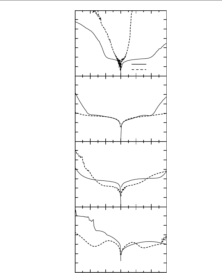
Fig. 9 shows the leakage current density as a function of applied electric field for 50 and 250
nm thick PZT films with various Zr/(Zr+Ti) ratio. We notice that PZT thickness and
Zr/(Zr+Ti) ratio influences leakage current density. Indeed, below 20% of Zr/(Zr+Ti) ratio,
the 250 nm thick films show higher current density than 50 nm thick sample [see Fig. 9(a)].
Increasing Zr/(Zr+Ti) ratio in films lead to a decrease of the leakage current density level in
the 250 nm thick PZT films from above 10
-3
A/cm² to 10
-6
A/cm² at an electric field of
100 kV/cm for Zr/(Zr+Ti) ratio ranging from 0.19 and 0.63 respectively.
Ferroelectrics - Characterization and Modeling
238
50nm
250nm
(a)
(b)
(c)
(d)
10
-9
10
-8
10
-7
10
-6
10
-5
10
-4
10
-3
Leakage current density (A/cm
2
)
10
-9
10
-8
10
-7
10
-6
10
-5
10
-4
10
-3
Zr/(Zr+Ti) ; 0.13
0.19
0.30
0.35
0.54
0.53
0.67
0.63
10
-9
10
-8
10
-7
10
-6
10
-5
10
-4
10
-3
-300 -200 -100 0 100 200 300
10
-9
10
-8
10
-7
10
-6
10
-5
10
-4
10
-3
Electric field (kV/cm)
Fig. 9. Leakage current density as a function of electric filed for 50 nm thick (plain line) and
250 nm thick (dotted line) PZT thin films with different Zr/(Zr+Ti) ratio: from small
Zr/(Zr+Ti) ratio (a) to large Zr/(Zr+Ti) ratio (d).