Jackson S.D., Hargreaves J.S.J. Metal Oxide Catalysis
Подождите немного. Документ загружается.

perovskite - like [WO
4
] layers and no superstructure forms. When half the W
6+
cations are substituted by Nb
5+
in this compound, the composition becomes
Bi
2
W
0.5
Nb
0.5
O
5.75
, with the two layered components being [Bi
2
O
2
]
2+
and
[W
0.5
Nb
0.5
O
3.75
]
2 −
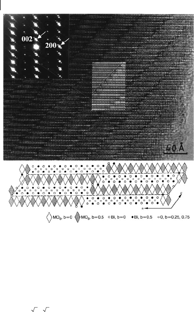
. The oxygen vacancies seem to enhance formation of a stepped
superstructure, which can release the charge separation [34, 35] (Figure 10.8 ).
Unfortunately, the oxygen positions cannot be determined by conventional
HRTEM, although those at the junctions of the steps are very important in
understanding the nature of the connection of the [Bi
2
O
2
]
2+
and [W
0.5
Nb
0.5
O
3.75
]
2 −
components in the ( ab ) planes.
Many Aurivillius phases have such stepped superstructures, which can only be
revealed by direct HRTEM imaging. Bi
5
Nb
3
O
15
has a structure with an intergrowth
of n = 1 and n = 2 Aurivillius members, [Bi
2
O
2
]
2+
[NbO
4
]
3 −
[Bi
2
O
2
]
2+
[BiNb
2
O
7
]
−
. Owing
to a greater charge separation, this compound forms a stepped superstructure even
without oxygen vacancies [36] .
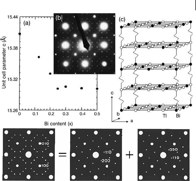
Figure 10.7 (a) The basic unit cell parameter
c via the nominal content of Bi in solid
solution Tl
1 −x
Bi
x
Sr
1.6
Ba
0.4
Ca
2
Cu
3
O
9
. (b) SAED
pattern of the solid solution specimen with
x = 0.3, viewed down the [001] zone axis.
(c) A 4 a × 4 b × 4 c superstructural model for
(Tl, Bi) - 1223 with the ratio Tl: Bi of 3 : 1. Only
the (Tl,Bi) – O layers are shown. The bottom
schematic drawing shows the division of the
SAED pattern in (b) into two simpler patterns
corresponding to 4 a × 2 b and 2 a × 4 b
supercells in the ( ab ) planes.
10.4 Superstructures 457
458 10 Transmission Electron Microscopy
Figure 10.8 HRTEM image of Bi
8
W
2
Nb
2
O
23
viewed down the
[010] zone axis of a Bi
2
WO
6
- like sub - cell. The insets show a
corresponding SAED pattern (top) and a simulated image
from a proposed model (bottom) with 8 nm specimen
thickness and 60 nm lens defocus. In the model, the M sites
are shared by W and Nb.
Charge separation can occur with the same type of cations. A well known
example is BaBiO
3
, which has a perovskite structure. The ideal basic unit cell is
cubic with a = 0.43 nm when all Bi cations are in a 4+ oxidation state. A charge
separation of Bi
5+
and Bi
3+
(believed to be the real oxidation states in BaBiO
3
)
leads to a
222××
monoclinic distorted superstructure with the supercell
parameters, a = 0.618 14, b = 0.613 60, c = 0.866 97 nm, and β = 90.173 ° [37] . This
superstructure was originally detected by XRD and can easily be confi rmed by
SAED.
10.4.2
Superstructures Based on Oxygen Ordering
In some oxides, formation of superstructures is merely due to oxygen ordering. A
good example was demonstrated by Reller and coworkers in 1984, by showing
many distinct superstructures in perovskite - type oxides CaMnO
3 − x
with oxygen
contents of 2.5, 2.556, 2.667, 2.75 and 2.80 [38] .
Another good example of oxygen ordering was found in YBaCo
2
O
5
. This com-
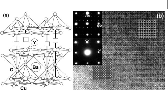
pound has a double - perovskite structure as shown in Figure 10.9 a, and contains
one Co
2+
and one Co
3+
per formula unit when the oxygen sites in the Y layer are
not occupied. Upon annealing the sample in pure oxygen, these sites will be par-
tially occupied by oxide anions, forming a 3 × 3 × 1 superstructure [39] , which can
be clearly shown by the SAED pattern along the [001] zone axis. An ideal model
has a unit cell composition of Y
9
Ba
9
Co
18
O
49
, in which the oxidation state of all Co
is close to 3+. Under electron beam irradiation, the extra oxygen in the Y layer was
removed and the diffraction spots corresponding to the superstructure in the
SAED patterns disappeared [40] .
In one study, Sr was introduced into YBaCo
2
O
5
to substitute Ba in order to tune
the space of the oxygen vacancies [9] . When the content of Sr in YBa
1 − x
Sr
x
Co
2
O
5+ δ
was increased, the ordering of extra oxygen reduced gradually as indicated by
SAED patterns, where the diffraction spots from the superstructure diffused
before completely disappearing. The high mobility of excess oxygen in YBaCo
2
O
5+ x
implies that this material may be developed into a good oxide ion conductor or
an oxide catalyst. The conductivity of some selected compositions of this solid
10.4 Superstructures 459
Figure 10.9 (a) Structural model of
YBaCo
2
O
5+x
, x = 0. Oxygen vacancies in the Y
layer are marked by squares. (b) HRTEM
image of the compound with x = 0.444,
viewed down the [001] direction. The top inset
is the corresponding SAED pattern. The SAED
pattern below was recorded after electron
beam irradiation with the screen brightness
of 150 PA cm
− 2
. Both patterns are indexed to
the basic unit cell shown in (a). Computer
simulated images were created with the
conditions of specimen thicknesses 0.76 (left)
and 3.8 nm (right); and lens defocuses − 40
(left) and − 70 nm (right).

460 10 Transmission Electron Microscopy
solution was measured with a maximum in conductivity in the range 180 – 320 ° C
indicating a form of metal - to - insulator transition at this temperature that is
unlikely to be related to a major change in oxygen content.
The perovskite - type structure is one of the most extensively investigated oxide
structures. Its ideal composition is ABO
3
. A is the large cation and B is the small
cation. In YBa
1 − x
Sr
x
Co
2
O
5
, A = Y, Ba, Sr (12 coordinated by oxygen) and B = Co
(octahedrally coordinated by oxygen). In addition to having a charge balance, the
formation of the perovskite structure should meet the requirement of the lattice
tolerance factor, t = 0.8 to 1.0, which is calculated from
t
RR
RR
=
+
+
()
ao
bo
2
where R
a
is the radius of the large cation, R
b
is the radius of the small cation and
R
o
is the radius of the oxygen anion (O
2 −
= 0.132 nm). When t is small, a very
common
222××
superstructure is developed due to lattice distortion (or rota-
tion of the MO
6
octahedra). For example, for CaMnO
3
the lattice tolerance factor
is about 0.85. The real structure is
222××
derived from the perovskite unit
cell [38] . The postulated perovskite unit, Ba
2+
Co
3+
O
3
in the YBa
1 − x
Sr
x
Co
2
O
5
solid
solution, has a tolerance factor of 0.965. No
222××
superstructure was
observed. On the other hand, the postulated perovskite units, Sr
2+
Co
2+
O
3
and
Sr
2+
Co
3+
O
3
have tolerance factors of 0.846 and 0.885, respectively. A SAED study
showed that a
222×× superstructure was gradually developed when the
content of Sr increased in the YBa
1 − x
Sr
x
Co
2
O
5
solid solution [9] . This is the most
commonly observed superstructure due to oxygen ordering in perovskite - type
oxides, even though there are no oxygen vacancies. The diffraction intensities
from such a superstructure are normally very weak and may not be observed
in XRD patterns. However, SAED can detect this type of superstructure easily.
Some example compounds are the perovskite - related Bi
3
Pb
2
Nb
2
O
11
Cl [41] and
RuSr
2
GdCu
2
O
8
[8] , as well as some ruthenocuprates such as Pb
2
RuSr
2
Cu
2
O
8
Cl and
(Ru,M)Sr
2
GdCu
2
O
8
(M = Sn, Nb) [42] .
10.4.3
Incommensurate Superstructures
An incommensurate superstructure is a superstructure derived from a basic struc-
ture without a proportional relation of dimensions to the basic unit cell. This type
of superstructure is often found in mixed oxides. A good example is Bi
2
O
3
- based
solid solutions.
When a small percentage of guest oxide, for example Nb
2
O
5
, is mixed with Bi
2
O
3
,
the high - temperature phase of δ - Bi
2
O
3
can be stabilized and several superstruc-
tures will be developed depending on the Nb
2
O
5
concentration [25] . Type I is a
2 × 2 × 2 commensurate superstructure with an ideal composition of Bi
30
Nb
2
O
50
,
which has been already mentioned previously in Section 10.4.1 . Further increasing
the Nb
2
O
5
content results in a type II incommensurate superstructure as shown
in Figure 10.10 .
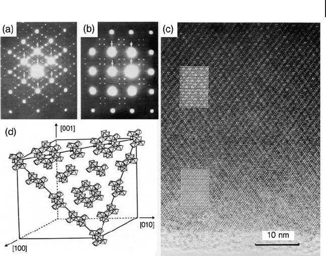
A cursory look at the SAED patterns (Figure 10.10 a and b) may give the impres-
sion that the dimensions of the superstructure are 3 × 3 × 3. However, careful
measurement of the positions of the superstructural diffraction spots can reveal
that the reciprocal spacing corresponding to these spots is disproportional to the
dimensions of the reciprocal basic unit cell [25, 32] . The HRTEM image in Figure
10.10 c shows a superstructural image contrast pattern. In fact, it is diffi cult to draw
a superunit cell for the whole crystal. In other words, the superstructure has no
long - range ordering. The reason for forming such a structure is that Nb
2
O
5
forms
some pyrochlore - like clusters in the δ - Bi
2
O
3
matrix as shown in Figure 10.10d and
these clusters are not perfectly ordered in a large area. These structural properties
cannot easily be determined by powder XRD, but are clearly shown in SAED pat-
terns and HRTEM images. To confi rm the proposed model for this type II super-
structure, a commensurate model must be used. It was found that the closest
commensurate superunit cell with an operable dimension is 8 × 8 × 8. The model
Figure 10.10 SAED patterns of Bi
8
Nb
2
O
17
solid solution along the (a) [110] and (b) [100]
zone axes. Maxima corresponding to the
δ - Bi
2
O
3
fl uorite sub - cell are shown by arrows.
(c) HRTEM image corresponding to (a). The
insets are computer simulated images using
the proposed commensurate 8 × 8 × 8
superstructural model shown in (d) with
conditions of specimen thickness of 4 nm and
defocus of 120 nm (nearer to the edge of the
crystal) and thickness of 8 nm and defocus of
140 nm (thick area). (d) Pyrochlore - type Nb - O
clusters in a (111) plane of the fl uorite - type
Bi
2
O
3
matrix.
10.4 Superstructures 461
462 10 Transmission Electron Microscopy
was successfully confi rmed by computer simulation of the HRTEM images and
SAED patterns [25, 32] . This type of incommensurate superstructure is also found
in the Bi
2
O
3
− Ta
2
O
5
system [30] .
Some incommensurate superstructures are developed from lattice distortion
instead of partial ordering of cations. One example is the superconducting oxide
Bi
2+ x
Sr
2
Ca
1 − x
Cu
2
O
8+ δ
[43, 44] .
10.5
Surface Profi le Imaging
The surface structures of oxide catalysts are important in the understanding of
their catalytic properties. HRTEM has been used to investigate the surface struc-
tures of oxides for many years, the method of HRTEM surface profi le imaging
having been introduced in the 1980s [45] . Unlike scanning tunneling microscopy
( STM ), which is also a direct imaging technique, HRTEM is not mentioned in
most surface science text books. Nevertheless, HRTEM is an important supple-
mentary technique in surface science. STM looks down a surface, giving 2D
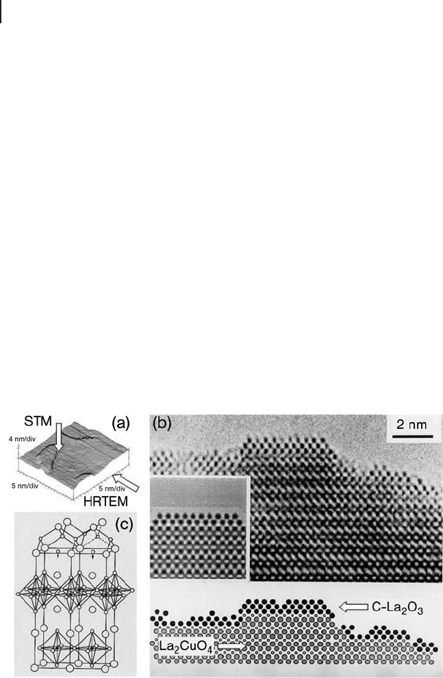
images, while HRTEM reveals the surface of solids in profi le (Figure 10.11 a). The
disadvantage of HRTEM is that only one - dimensional information of a surface can
be obtained. On the other hand, HRTEM surface profi le imaging provides surface
Figure 10.11 (a) Schematic drawing of the viewing directions
of STM and HRTEM for a solid surface; (b) HRTEM surface
profi le image of the (001) surface of La
2
CuO
4
showing a
different image contrast pattern at surface in comparison with
that in the bulk. The inset is a computer simulated image
using a model shown in (c).
structural information as well as subterranean structures of solids. The surface -
related properties of materials can therefore be better understood [46] . There are
several other advantages of surface investigation by HRTEM. For example, speci-
men preparation is simple. Normally, small particles with any size and any mor-
phology can be directly used. Multiple scattering can normally be ignored, since
the surface areas are often very thin and can legitimately be treated as “ weak
phase ” objects, where the image intensity indicates the projected electrostatic
potential.
Figure 10.11b shows a typical HRTEM surface profi le image of La
2
CuO
4
. It was
found that the image contrast pattern in the top surface layers is different from
that in the bulk area. Image simulation revealed that the (001) surface of La
2
CuO
4
crystals was frequently coated by several atomic layers of C - La
2
O
3
[47, 48] .
HRTEM profi le imaging can reveal many surface microstructures. For example,
many high Tc superconducting crystals suffer from surface decomposition and an
amorphous coating layer can be observed. If this surface coating layer has the
same composition as the parent compound, the coating can recrystallize under
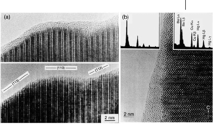
electron beam irradiation. Figure 10.12 a shows a YBa
2
Cu
3
O
7
crystal with surface
decomposition into an amorphous layer of about 2 nm thickness, and an image of
the same specimen area after recrystallization of the coating layer under the elec-
tron beam irradiation [49, 50] . Similar phenomena were also observed from other
10.5 Surface Profi le Imaging 463
Figure 10.12 (a) HRTEM images of
YBa
2
Cu
3
O
7 −δ
, viewed down the [110] direction.
The initial image showing a thin layer of
disordered coating, and the image recorded
from the same area after electron beam
irradiation for 3 h. The disordered layer
recrystallized into a clean crystalline surface.
The (113), (110) and (112) crystal planes on
the surface are indicated. (b) HRTEM image
of HgBa
2
CuO
4+δ
viewed down the [010]
direction, showing a disordered coating on
the (100) surface. The insets are EDS spectra
from the surface area (top left) and the
interior area (top right).

464 10 Transmission Electron Microscopy
high Tc superconducting oxides [51 – 54] . To make sure that recrystallization only
takes place at the interface of the crystal and the amorphous layer, the beam bright-
ness should be carefully controlled to allow a lengthy process. Otherwise, individ-
ual nanocrystallites of metal oxides, for example copper oxide and barium oxide,
may be created in the amorphous layer. On the other hand, if the composition of
the decomposed surface coating layer changes, the amorphous layer cannot be
repaired. For example, the surface of HgBa
2
CuO
4+ δ
crystals is often decomposed
by loss of Hg as detected by a narrow electron beam EDX analysis (Figure 10.12 b)
[55] . This amorphous layer cannot recrystallize into the parent crystal, although
formation of barium copper oxide microcrystallites is still possible. The surface
crystallinity of these high Tc superconducting materials certainly affects the physi-
cal properties of the materials [56] .
It is worth mentioning that a very small electron beam, for example about 2 nm
in the case in Figure 10.12 b for HgBa
2
CuO
4+ δ
, should be used in EDX. The collec-
tion time for the EDX spectrum shown in the left inset was several hours, while
the EDX spectrum in the right inset was obtained in only a few minutes. During
such a long collection time, the operator must make sure that the beam location
is always at the surface amorphous region. Narrow beam diffraction patterns may
help in this respect. When the beam is very small, different diffraction patterns
from different areas can be observed. From the crystalline region, a single crystal
pattern with individual diffraction disks is shown. The pattern from the disordered
region shows one or more diffraction rings. When the beam shifts away from the
particle, no diffraction signals can be observed. Exposing the specimen area to an
electron beam for a long time may result in heavy carbon contamination. The
beam location at the amorphous layer should therefore be moved many times
along the surface.
When a clean surface of a crystallite is observed without any coating layer, it is
possible to determine the terminal atomic planes on various crystal surfaces. For
example, three distinct surface terminal planes are marked in Figure 10.12 a.
HRTEM studies of the [001] surface of YBa
2
Cu
4
O
8
by examination of profi le
images indicated that the surface usually terminated with the CuO
2
plane corre-
sponding to a sequence of bulk – Y – CuO
2 − x
, while the [001] surface of YBa
2
Cu
3
O
7
prefers to terminate with the BaO atomic plane [57] . Zandbergen investigated a
CuO terminal plane on the [001] surface of GdBa
2
Cu
3
O
7
and found that the ter-
minal atomic plane often had a different image contrast indicating lattice distor-
tion including surface relaxation [58] , especially when oxygen in the termination
plane was partially lost.
By exposing a clean crystal surface to the electron beam, a series of HRTEM
surface profi le images can be recorded and a movement of surface atoms from a
high - energy site to a low - energy site may be observed [47] .
Observation of various surface defects is an important topic in HRTEM surface
profi le imaging. In Figure 10.11 b, it can be seen that over a large area the coating
layer of C - La
2
O
3
is not continuous. Instead, the coating layer is broken into some
small islands. This is because the lattices of C - La
2
O
3
and La
2
CuO
4
as shown in
Figure 10.11 c do not match each other perfectly. Very interesting surface profi le

images of CeO
2
observed by Jacobson and coworkers showed sharp microfaceting
on the surface of the CeO
2
fi lm, indicating that nominally designated crystallo-
graphic surfaces might not coincide with the as - grown surfaces [59] .
When HRTEM is used for examining nanoparticles of oxides, in which the
proportion of surface area greatly increases, most structural information concerns
the surface. For example, HRTEM images of core – shell quantum dots can show
the shell structure and its thickness directly. HRTEM images of metal oxide nano-
tubes can also be regarded as surface profi le images. The application of TEM in
nanomaterials will be further discussed below.
10.6
Defects in Oxides
General speaking, a crystal defect is a type of microstructure in which the parent
crystal structure is locally disturbed. Such a microstructure cannot be described
by a superstructure, even by an incommensurate superstructure. Since the defect
areas are usually very small, they may not be detected by XRD and neutron dif-
fraction methods. HRTEM is the most powerful technique to detect them and to
investigate their relation with the parent crystals. The defects can greatly change
the properties of an oxide. Some examples of the common defects in oxides are
given in the following sub - sections.
10.6.1
Layered Defects
Layered defects often form in layered oxides when several different, but closely
related, phases intergrow together in a disordered manner. In the high Tc super-
conducting oxide series Tl
2
Ba
2
Ca
n − 1
Cu
n
O
2 n +4
, n can vary from 1 to 4. The half unit
cells of all these members contain a [Tl
2
Ba
2
O
4
] layer and a [Ca
n − 1
Cu
n
O
2 n
] perovskite -
like block. Therefore, they have a tetragonal structure with similar a dimensions
( ∼ 0.385 nm) and different c dimensions, 2.323 nm ( n = 1), 2.931 nm ( n = 2),
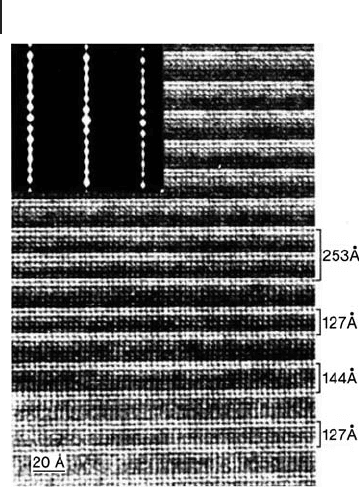
3.588 nm ( n = 3) and 4.160 nm ( n = 4). It is easy to form disordered intergrowth
along the c axis as shown in Figure 10.13 [19] .
The corresponding SAED pattern in Figure 10.13 shows diffused diffraction
spots along the c axis. As described above, a superunit cell can be drawn from a
superstructure. SAED patterns of incommensurate superstructures also show
sharp diffraction spots. Therefore, an approximate unit cell can be suggested for
image simulation and for studying its structural principle. However, it is impos-
sible to fi gure out a unit cell from the SAED and the image in Figure 10.13 . We
have to analyze individual layered components if we are to understand the whole
structure.
Another well known layered defect is the so - called stacking fault, often forming
in close - packed structures of metals. This is because ccp and hcp have a very small
energy difference. They can intergrow along the [111] axis (ABCABC stacking) of
10.6 Defects in Oxides 465
466 10 Transmission Electron Microscopy
the cubic phase and the [001] axis of the hexagonal phase (ABAB stacking) to share
identical planes. Such a defect is uncommon in metal oxides, although it has been
detected in some zeolites. Recently, stacking fault defects have been observed in
face centered cubic or hexagonal mesoporous silica, in which the pore arrange-
ments can be regarded as close - packed structures [60] .
10.6.2
Twin Defects
YBa
2
Cu
3
O
7
is orthorhombic, with unit cell parameters a = 0.381, b = 0.388 and
c = 1.163 nm. The reason for the difference between a and b is that there is a
Cu – O chain along the b axis and, in the same layer, oxygen vacancies are located
between Cu atoms along the a axis. But the oxygen can easily move from the b
axis to the a axis, equivalent to a rotation of the unit cell around the c axis by
90 ° , as shown by a model in the inset of Figure 10.14 a. The thick line indicates
the twin plane. Domains on the two sides of this plane have mirror symmetry.
When the domains are large, low magnifi cation TEM images may show a strong
contrast pattern (Figure 10.14 a), mainly attributed to diffraction contrast [61] .
Figure 10.14 b shows a HRTEM image of YBa
2
Cu
3
O
7
with microtwin defects,
where the domain sizes are very small.
Figure 10.13 HRTEM image of a specimen in
Tl
2
Ba
2
Ca
n − 1
Cu
n
O
2n +4
with a nominal composition with n = 2,
viewed down the [100] direction. A disordered intergrowth of
different members is shown. The inset is the corresponding
SAED pattern
