Henini M. Handbook of Self Assembled Semiconductor Nanostructures for Novel devices in Photonics and Electronics
Подождите немного. Документ загружается.

InAs Quantum Dot Formation Studied at the Atomic Scale 179
mobility of In on AlAs, explains the homogeneous indium distribution in the base of the InAs/AlAs
QDs. It has been proposed that the growth of dots on AlAs is initiated by 2D islands which develop into
small 3D islands for higher InAs depositions [52] . This is in contrast with the growth of dots on GaAs
where dot formation is initiated by small indium-rich nucleation centres which develop into trum-
pet-shaped indium distributions by the preferential diffusion of In to the apex of the dot [26] . These
growth mechanisms are supported by our observation of the indium distribution inside the dots.
The observed decrease of the indium concentration towards the top of the InAs/AlAs QD
might be caused by the residual incorporation of AlAs in the top of the dot during the capping
process. In order to reduce the total strain fi eld in the QD some capping material is incorporated
in the top of the dot. In the case of GaAs capping, the diluted part of the dot is very mobile and
therefore disappears very quickly during capping, causing levelling of the QDs. The InAs diluted
by Al, however, is much less mobile due to the stronger Al–In bond strength and therefore more
diluted material at the top remains in place.
In Fig. 5.15e and f we show measured and calculated relaxation profi les of segregated WLs in
GaAs and AlAs that were grown at a higher temperature of 530°C. These WLs did not show dot
formation. The indium segregation profi le of the WLs can be simply described by the phenom-
enological model of Muraki et al . described in the previous section [27, 31]. Based on this model,
we calculated the outward relaxation of the WLs using the analytical expressions by Davies et al.
[24] . The optimal fi t to the experimental relaxation profi les was obtained with N ( 1 . 9 0.1) ML ,
R 0 . 7 9 0.03 and N ( 1 . 9 0.1) ML , R 0.78 0.03 for the InAs WLs in GaAs and AlAs,
respectively, where N is the total amount of deposited In and R the segregation coeffi cient. The
obtained values for N are in agreement with the nominal deposited amount of indium. We do not
fi nd a signifi cant difference in the segregation coeffi cients of indium in AlAs and GaAs as was con-
cluded by Schowalter et al. [27] . The small apparent difference between the relaxation profi les of
the WLs can be attributed to the difference in lattice constants of GaAs and AlAs. We conclude that
InAs segregation does not play a role in the difference in the formation of QDs in AlAs and GaAs.
In summary, InAs QDs grown on GaAs are larger than those grown on AlAs, and they show
both a lateral and a normal gradient in the In composition, while InAs/AlAs QDs show only a
vertical gradient and with an opposite sign (In concentration decreasing from bottom to top).
The WLs on GaAs and AlAs do not show signifi cant differences, so we suggest that the segre-
gation of the WL is mainly strain driven, whereas the formation of the QDs is also determined
by growth kinetics. In particular, the observed differences between QDs are due to the reduced
mobility of In in AlAs due to the higher Al–In bond strength, which modifi es both the QD forma-
tion and capping processes.
5.4 Capping process of InAs quantum dots
In previous sections we have studied relevant aspects of the WL and QD formation process.
Nevertheless, once created, the QDs are subsequently capped, a step which is required for any
device application. Although a lot of effort has been dedicated to understand the QD growth
mechanism, there are relatively few studies focused on the effect of the capping process [12–20] .
Some of these studies have already shown signifi cant differences in size, shape and composition
between uncapped and capped QDs. For example, an important collapse of the QD height has
been reported for InAs/GaAs QDs capped with GaAs [14, 15, 17–19] , revealing the big infl uence
of the capping process on the structural properties of the QDs.
In this section we use X-STM to analyse the capping process of InAs QDs. The effect of the cap-
ping temperature and growth interruptions is studied, as well as the impact of using different
materials in the capping layer. The possibility of controlling the QD height with a double capping
method is also discussed.
5.4.1 Capping temperature and growth interruptions
Levelling of InAs/GaAs QDs after deposition of thin GaAs cap layers has been clearly revealed by
top-view STM [18, 58] and atomic force microscopy (AFM) [54] . The levelling process has been
CH005-I046325.indd 179CH005-I046325.indd 179 6/27/2008 4:19:31 PM6/27/2008 4:19:31 PM
180 Handbook of Self Assembled Semiconductor Nanostructures for Novel Devices in Photonics and Electronics
attributed to the additional strain build-up between the cap layer and the partially relaxed InAs
QDs [18, 54] to destabilize the QDs. These experiments, however, lack information about the
shape and, in particular, the residual height of the QDs which is the most important parameter
determining the electronic properties. In this section, we study the GaAs-capping process of InAs
QDs on GaAs(100) by X-STM. The role of the capping temperature and growth interruptions is
discussed. Detailed and accurate results of the QD levelling are presented, which are essential for
understanding the capping process and the control of the structural and electronic properties of
InAs QDs.
The samples were grown by solid source MBE on Si-doped n -type GaAs(100) substrates. After
oxide desorption at 580°C, a 150 nm thick GaAs buffer layer was grown. Then the substrate tem-
perature was lowered to 500°C for deposition of 2.1 ML InAs. Formation of InAs QDs was verifi ed
by the sharp transition from streaky to spotty of the refl ection high-energy electron diffraction
pattern. Thereafter, for samples A–D different capping procedures were applied: (A) deposition of
10 nm GaAs at 500°C followed by 150 nm GaAs growth at 580°C; (B) cooling down the sample
to 300°C before capping the InAs QDs by 10 nm GaAs at the same temperature and growth of
150 nm GaAs at 580°C; (C) capping the InAs QDs by 3 ML GaAs at 500°C, then cooling down
the sample to 300°C for deposition of 150 nm GaAs; and (D) capping the InAs QDs by 3 ML GaAs
at 500°C followed by a growth interruption (GI) of time t , deposition of 10 nm GaAs at the same
temperature, and growth of 50 or 150 nm GaAs at 580°C. In sample D fi ve such InAs QD layers
were inserted with GI times t of 0, 20, 40, 60, and 90 seconds, separated by 60 nm GaAs. An
extra 30 nm GaAs spacer was grown as a marker between the QD layers with GI times t of 40
and 60 seconds. The time for cooling down samples B and C from 500 to 300°C was 4 minutes.
The growth rates were 0.58 and 0.06 ML/s for GaAs and InAs, respectively, and the As
4
beam
equivalent pressure was 1 10
5
torr.
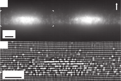
Figure 5.16a shows the fi lled state’s topography X-STM image of the InAs QDs in sample A
which are capped in the conventional way by 10 nm GaAs at 500°C and 150 nm GaAs at 580°C.
The marked part of the image is shown in Fig. 5.16b after treatment with a local mean equaliza-
tion fi lter [55] to enhance atomic details by removing the large scale background contrast. The
bright horizontal lines are the top zig-zag rows of the (110) surface, which are separated by one
bilayer (BL), i.e. two MLs. The topographical contrast in Fig. 5.16a is due to the outward relaxa-
tion of the cleaved surface of the compressively strained InAs QDs, revealing their cross-sectional
shape. The bright spots in Fig. 5.16b correspond to In atoms in the top layer of the cleaved sur-
face. The height of the InAs QDs in sample A is measured as 8 BLs by counting the number of
atomic rows.
(a)
(b)
5 nm
5 nm
Figure 5.16 (a) Filled states topography X-STM image of the InAs QDs in sample A with conventional capping by
10 nm GaAs at 500°C and 150 nm GaAs at 580°C. V
sample
3.0 V. A part of the image (a) marked by four cor-
ners is treated by a local mean equalization fi lter and shown in (b). In (a) the arrow indicates the growth direction.
The black-to-white height contrast in (a) is 0 to 0.5 nm.
CH005-I046325.indd 180CH005-I046325.indd 180 6/27/2008 4:19:31 PM6/27/2008 4:19:31 PM
InAs Quantum Dot Formation Studied at the Atomic Scale 181
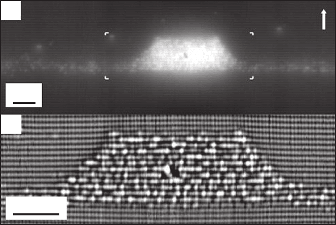
It is well established that InAs QDs buried in the conventional way of sample A exhibit a reduced
height compared to unburied ones due to QD levelling [18, 53, 54] . In order to determine the QD
height reduction, the shape change during overgrowth of the InAs QDs in sample B is strongly
suppressed by capping them at 300°C. The fi lled state’s topography X-STM image of an InAs QD
in sample B is shown in Fig. 5.17a with the fi ltered image in Fig. 5.17b . The InAs QD exhibits very
sharp and well-defi ned interfaces confi rming the suppressed QD levelling, atom diffusion, and seg-
regation [29] and, thus, the preservation of the QD shape [56, 57] . The height of the InAs QD is
12 BLs which is 4 BLs larger than that of the QDs in sample A. This indicates that during conven-
tional capping at 500°C the QD height is reduced by about one third of the original one.
(a)
(b)
5 nm
5 nm
Figure 5.17 (a) Filled states topography X-STM image of the InAs QD in sample B with the GaAs cap grown at
300°C. V
sample
3.0 V. A part of the image (a) marked by four corners is treated by a local mean equalization
fi lter and shown in (b). In (a) the arrow indicates the growth direction. The black-to-white height contrast in (a) is 0
to 0.5 nm.
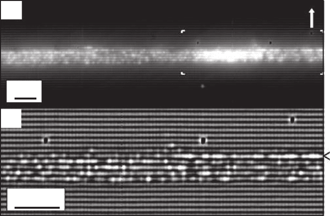
When InAs QDs are capped only by a very thin GaAs layer, strong QD levelling or QD collapse
occurs. Figure 5.18 shows the fi lled state’s topography and fi ltered images of such InAs QDs in
sample C. The QDs are capped at 500°C by 3 ML GaAs and subsequently overgrown at 300°C to
further maintain the shape. During the thin GaAs capping and cooling down, the levelling of the
InAs QDs leads to a rather homogeneous (In,Ga)As layer in between the QDs due to In detachment
from the QD tops, Ga/In intermixing, and In segregation with a thickness of about 4 BL, which
is much thicker than the original InAs wetting layer. Intermixing with the GaAs substrate [58]
expected during the growth of InAs at 500°C additionally contributes approximately 3 ML of GaAs
to the (In,Ga)As layer, which is derived by subtracting the thicknesses of deposited InAs (2.1 ML)
and GaAs (3 ML) from the total (In,Ga)As thickness of 4 BL. After levelling of the QDs, unincorpo-
rated In fl oating on the surface is pinned there by the low-temperature GaAs capping and forms an
In-rich layer marked by the arrow in Fig. 5.17b . The sharp interface between this layer and the low-
temperature GaAs cap confi rms that In segregation and diffusion in growth direction are strongly
suppressed for GaAs overgrowth at 300°C. Most interestingly, the InAs QDs are completely levelled
to the thickness of the (In,Ga)As layer in between them, which is much smaller than the height of
the QDs observed in sample A. This suggests that the conventional, continuous GaAs capping at
500°C in sample A not only drives QD levelling during the initial stage, like the thin GaAs capping
in sample C, but also quenches the levelling process when the QDs become buried.
CH005-I046325.indd 181CH005-I046325.indd 181 6/27/2008 4:19:32 PM6/27/2008 4:19:32 PM
182 Handbook of Self Assembled Semiconductor Nanostructures for Novel Devices in Photonics and Electronics
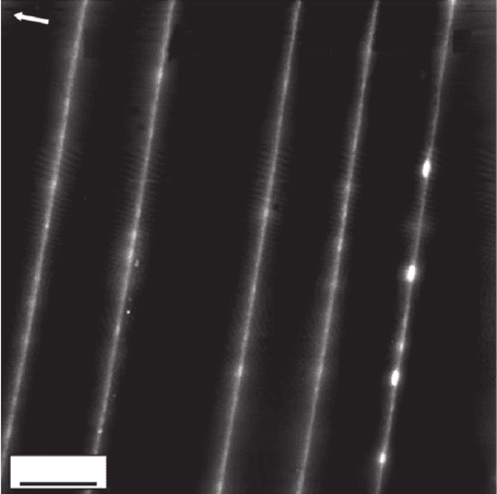
To assess the time scale of QD levelling which is, thus, crucial for the fi nal size and shape of the
buried QDs, varying GI times are inserted in sample D after deposition of 3 ML GaAs at 500°C on
the InAs QDs prior to GaAs overgrowth. Figure 5.19 shows the fi lled state’s topography image
of the InAs QDs in sample D with GI times of 0, 20, 40, 60, and 90 seconds in subsequent lay-
ers. Clearly, the height of the InAs QDs capped without GI (fi rst layer) is signifi cantly larger than
that of the QDs with insertion of 20 seconds GI. No signifi cant further decrease in QD height
is observed when the GI time is increased to 90 seconds. Hence, QD levelling during thin GaAs
capping and GI takes place on a time scale of less than 20 seconds. For the present GaAs growth
rate, this is comparable to the time required for growing several nanometres of GaAs to fully bury
the QDs by continuous overgrowth. This indicates that both the driving and quenching of the QD
levelling in conventional capping take place on a similar timescale. The size and shape of the bur-
ied QDs are therefore determined by a delicate interplay between driving and quenching of the
QD levelling which is controlled by the GaAs growth rate and growth temperature.
A model based on the above experimental results is proposed for the growth of InAs QDs embed-
ded in GaAs. The growth of InAs commences in the two-dimensional (2D) layer-by-layer mode
until the InAs thickness reaches the critical value of 1.7 ML for InAs QD nucleation to reduce the
accumulated strain. The InAs QDs are formed by In atoms transported massively from the 2D
InAs layer, leaving a thin wetting layer on the surface. The whole system is stable at the minimum
of the total energy composed of the surface energy, the strain energy, and the interface energy.
Subsequent capping of the InAs QDs by GaAs, on the other hand, introduces extra strain energy
between the GaAs cap and the InAs QD layer, resulting in an unstable system and the consequent
QD levelling process. In atoms are redistributed from the InAs QD tops to the areas in between
them during the QD levelling. They contribute to a several nanometres thick (In,Ga)As layer with
an exponential In composition decay due to In segregation and Ga/In intermixing during over-
growth [28] , reducing the lattice mismatch and, hence, the total energy of the system. Thus, the
thickness and the In composition profi le of the (In,Ga)As layer in between the InAs QDs strongly
depends on the QD levelling and In segregation. It is important to note that the QD levelling is
very sensitive to the substrate temperature and is strongly suppressed at low growth tempera-
tures, where it becomes more and more diffi cult to thermally break the In-As bonds. In addition to
(a)
(b)
5 nm
5 nm
Figure 5.18 (a) Filled states topography X-STM image of the InAs QD in sample C capped by 3 ML GaAs at
500°C, followed by 150 nm GaAs grown at 300°C. V
sample
3.0 V. A part of the image (a) marked by four cor-
ners is treated by a local mean equalization fi lter and shown in (b). In (a) the arrow indicates the growth direction.
The black-to-white height contrast in (a) is 0 to 0.4 nm.The arrow in (b) points to the In-rich layer.
CH005-I046325.indd 182CH005-I046325.indd 182 6/27/2008 4:19:33 PM6/27/2008 4:19:33 PM
InAs Quantum Dot Formation Studied at the Atomic Scale 183
inducing QD levelling, the GaAs cap buries the InAs QDs, thereby quenching the levelling process
during continued overgrowth. Therefore, the size and shape of the embedded InAs QDs are deter-
mined by a delicate interplay between driving and quenching of the QD levelling during capping,
which depends strongly on the growth rate and growth temperature of the GaAs cap.
In summary, we have investigated the GaAs-capping process of InAs QDs grown by molecular-
beam epitaxy on GaAs(100) substrates. In its initial stage, GaAs capping induces levelling of the QDs
to drastically decrease their height. During continuous capping the QD levelling is quenched when
the QDs become buried. Both phenomena, driving and quenching of the QD levelling, take place on
a similar time scale and are very sensitive to the GaAs growth rate and growth temperature. This
understanding opens up an effi cient route for controlling the size and shape of buried QDs.
5.4.2 Capping with different materials
We have seen how the QD structure is strongly affected by capping with GaAs and how this proc-
ess is very sensitive to the growth temperature and growth interruptions. Since GaAs is the most
commonly used capping material for InAs/GaAs QDs, the existing structural studies of buried
InAs/GaAs QDs have been mainly devoted to GaAs-capped QDs. Nevertheless, different materials
such as InGaAs and GaAsSb are nowadays used to cap InAs/GaAs QDs in an effort to extend its
emission wavelength to the technologically interesting 1.3–155 μ m region [59–64] . For InAs/
InP QDs, capping materials other than InP, like InGaAsP, have also successfully been used for
laser applications [65–67] .
The use of different capping materials strongly affects the emission wavelength and therefore
should strongly affect the QD electronic and/or structural properties, such as size, shape, compo-
sition, strain, band offsets, etc. Indeed, critical issues occurring during capping like dot decom-
position, intermixing, segregation, As/P exchange and phase separation in the capping layer
depend on the capping material. To understand the impact of the capping material on the struc-
tural properties of the QDs is consequently of crucial importance.
In this section, we have used X-STM to analyse at the atomic scale how capping with differ-
ent materials infl uences the structural properties of InAs QDs in GaAs and InP. The role of the
50 nm
90 60 40 20 0
Figure 5.19 Filled states topography X-STM image of the fi ve InAs QD layers in sample D. The InAs QDs are
capped by 3 ML GaAs at 500°C, followed by a GI and a 10 nm GaAs cap grown at 500°C plus a GaAs separation
layer at 580°C. V
sample
3.0 V. The increasing GI times of 0, 20, 40, 60, and 90 seconds are noted in the image.
The arrow indicates the growth direction. The black-to-white height contrast is 0 to 0.5 nm.
CH005-I046325.indd 183CH005-I046325.indd 183 6/27/2008 4:19:34 PM6/27/2008 4:19:34 PM
184 Handbook of Self Assembled Semiconductor Nanostructures for Novel Devices in Photonics and Electronics
different effects occurring during capping (intermixing, segregation, As/P exchange, compo-
sitional modulation in the capping layer, etc.) is determined. First, we study the capping with
strained layers to reveal the role of strain. For that we used InAs QDs grown on (100) GaAs
capped with InGaAs and GaAsSb strain reducing layers. Then we study the capping with lattice
matched layers (with respect to the substrate), where the chemical effects could dominate the
process. For that we study InAs dots grown on (311)B InP that were capped by either InP, InGaAs
or InGaAsP (the last two materials being nominally lattice matched to InP). While strong mor-
phological differences are found when strained layers are used, the difference between various
lattice-matched capping materials is more subtle, although also relevant for device applications.
5.4.2.1 Capping with strained layers
When InAs/GaAs QDs are capped with a material which has a larger lattice constant than GaAs
(and consequently closer to the one of InAs), the strain induced in the dot during capping could
be smaller, which would red shift the emission wavelength. In addition, the modifi ed strain differ-
ence could induce differences in dot size, shape and composition since dot decomposition during
capping could be infl uenced by the strain. This is what we analyse in this section.
5.4.2.1.1 InGaAs capping of InAs/GaAs QDs
Capping with InGaAs has become popular in the last few years because it allows the emission
wavelength of InAs/GaAs QDs [59–63] to be increased considerably. It is therefore very interest-
ing to study how the structural properties of InAs QDs are affected by an InGaAs strain reducing
layer.
The sample used in this study was grown by solid source MBE on an n
Si-doped (100) GaAs
substrate. 2.7 MLs of InAs were deposited at 500°C and 0.1 ML/s on an intrinsic GaAs buffer
layer. The QD layer was capped with a nominally 6 nm thick In
0.15
Ga
0.85
As layer grown at 500°C
at a growth rate of 0.5 ML/s.
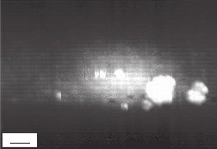
Figure 5.20 shows a high voltage fi lled states image of an InAs/GaAs QD capped with InGaAs.
The InGaAs layer is not well appreciated in this image because the contrast is dominated by the
cleavage induced defects close to the dot. The dot is 7.0 0.5 nm high, considerably higher than
the typical GaAs-capped QDs, which are 3–5 nm high, as shown in previous sections [15, 18, 19].
Nevertheless, the top facet is not as well defi ned as in the GaAs case and the In content decreases
gradually in the growth direction (that is why the error in determining the height is larger).
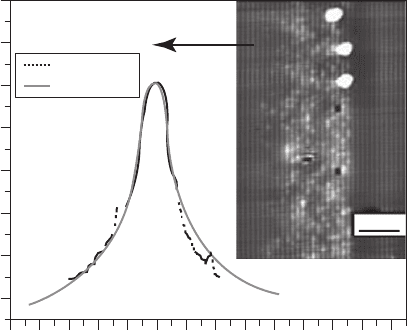
The In composition in the capping layer was deduced by the analysis of the outward relaxation.
The fi t shown in Fig. 5.21 was found when an 8.5 nm thick layer (as measured from the X-STM
images) with 17% In content is considered in the calculation. The In content is close to the nomi-
nal value (15%), although the layer is considerably thicker than the nominal 6 nm. The lattice
5 nm
Figure 5.20 Topography image of an InAs/GaAs QD capped with InGaAs ( V 3 V , I
tunnel
55 pA). The big
white regions are cleavage induced defects. Growth direction: [001], lateral direction: [110].
CH005-I046325.indd 184CH005-I046325.indd 184 6/27/2008 4:19:35 PM6/27/2008 4:19:35 PM
InAs Quantum Dot Formation Studied at the Atomic Scale 185
mismatch between InAs and the capping layer is now 0.056, about 17% smaller than in the case
in which GaAs capping is used. We think that the reduced dot decomposition during capping is
related to this smaller lattice mismatch; the result is that the dot height is increased by factor
of ⬃ 2 compared to GaAs capping. This interpretation is in agreement with previously reported
results in which QDs capped with InGaAs instead of GaAs are shown to retain their shape dur-
ing the initial stages of capping [71, 72] . It could be argued that the increase in dot height is
due to strain induced compositional modulation in the capping layer [68] . Although part of the
increase in dot height could be due to that effect, we think that its contribution should be very
small, since no traces of compositional modulation are observed in the capping layer. The role of
the strain can be clarifi ed by using GaAsSb as the capping material, because in this case the InAs
dot height cannot increase due to phase separation in the capping layer.
2010
0.05
0.10
0.15
0.20
0.25
0.30
0.35
0.40
Growth
direction
Outward relaxation (nm)
10 20 30 40 50
z (nm)
60 70 80 90 100 110
5 nm
0
Theoretical
Experimental
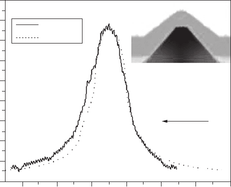
Figure 5.21 Measured (dotted line) and calculated (solid line) outward relaxation profi les of the InGaAs capping
layer. A 8.5 nm thick layer (as measured from the images) with a 17% In content was considered in the calculation.
The inset shows a high-pass fi ltered topography image of the InGaAs capping layer ( V 3 V , I
tunnel
55 pA). The
big white regions are cleavage induced defects.
5.4.2.1.2 GaAsSb capping of InAs/GaAs QDs
In the last few years, GaAsSb capping layers have also been used to increase the emission wave-
length of InAs/GaAs QDs [63, 69] and room temperature photoluminescence at 1.6 μ m has
recently been reported from GaAsSb-capped In(Ga)As/GaAs QDs [64, 70] . The strong red shift
observed by using GaAsSb instead of GaAs capping layers has been attributed to a type II band
alignment [64, 70] . However, the structural properties of these QDs have not been studied,
despite the fact that they could be signifi cantly different from those of GaAs-capped QDs. Due to
the larger lattice constant of GaAsSb compared to GaAs, the strain induced in the dot during
capping could be smaller, which would further red shift the emission wavelength and could affect
the dot size, shape and composition, as was the case with InGaAs capping.
The studied samples were grown by solid source MBE on n
Si-doped (100) GaAs substrates.
In the fi rst sample (sample A), 2.7 monolayers (ML) of InAs were deposited at 500°C and
0.1 ML/s on an intrinsic GaAs buffer layer. The QDs were capped with a nominally 6 nm thick
GaAs
0.75
Sb
0.25
layer grown at 475°C. In the second sample (sample B), two QD layers were
grown under the same conditions (2.7 ML of InAs deposited at 500°C and 0.1 ML/s). The fi rst
layer was capped with GaAs, and the second with 6 nm GaAs
0.75
Sb
0.25
. The capping tempera-
ture was 500°C in both cases. A layer of surface QDs was also grown for atomic force microscopy
measurements.
CH005-I046325.indd 185CH005-I046325.indd 185 6/27/2008 4:19:35 PM6/27/2008 4:19:35 PM
186 Handbook of Self Assembled Semiconductor Nanostructures for Novel Devices in Photonics and Electronics
A number of individual QDs were analysed in sample A in order to extract information con-
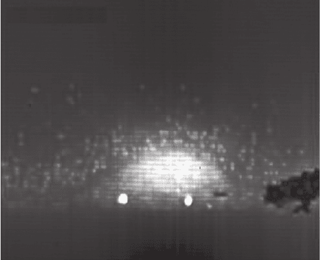
cerning their size, shape and composition. Figure 5.22 shows a high voltage fi lled states topog-
raphy image of a QD in this sample. The group V elements are imaged in this measurement so
that the bright spots are Sb atoms in the As matrix. Sb segregation into the GaAs layer is clearly
observed. Contrary to what happens when capping with GaAs at similar temperatures [12] , the
capping layer covers all of the dot. This behaviour cannot be attributed to a larger bond strength
preventing Ga migration on the growth surface, since the Ga–Sb bond is weaker than the Ga–As
one (45.9 and 50.1 Kcal/mol, respectively). The reason is likely to be the smaller strain that exists
between the partially relaxed InAs QDs and the GaAsSb capping layer. This smaller strain can
be accommodated by the system at the present growth temperature (475°C) without inducing
the migration of capping material away from the top of the dots. The dot is a full pyramid with a
diagonal base length of 32 2 nm. The height is 9.5 0.2 nm, much larger than that of typical
GaAs-capped QDs (3–5 nm high) [15,18,19] . This result indicates that the QDs are not dissolved
during capping with GaAsSb.
50 nm 41 nm
Figure 5.22 Filled states topography image of an InAs/GaAs QD capped with GaAsSb ( V 3 V). The bright
spots are Sb atoms in the As matrix. The white circles and the dark feature are cleavage induced defects.
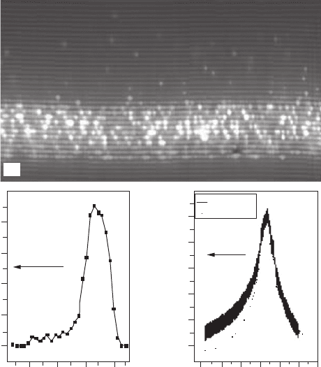
The Sb composition in the capping layer can be obtained directly by counting the individual
Sb atoms in the fi lled states images, for example Fig. 5.23a . The Sb concentration profi le as a
function of distance along the growth direction is plotted in Fig. 5.23b . The average Sb content
is 22%. This result can be checked by also analysing the outward relaxation of the cleaved sur-
face. The relaxation of the capping layer was compared to calculations from continuum elastic-
ity theory. The fi t shown in Fig. 5.23c was obtained for a 5 nm thick layer (as measured from
the X-STM images) with a 25% Sb composition. The agreement between theory and experiment
is quite good in the region of the layer itself, but deviates above the layer. This deviation is due
to the effect of Sb segregation, which is not included in the model but is clearly present in the
structure (see Fig. 5.23a and the asymmetry in the Sb profi le obtained by atom counting).
The obtained Sb concentration of 22–25% agrees well with the nominal growth value. The
lattice mismatch between this GaAsSb composition and relaxed InAs is 0.048, about 28% smaller
than in the case in which GaAs capping is used. We propose that the fact that dot decomposition
during capping is suppressed is related to the reduced strain between the dot and the capping
layer, although chemical effects due to the presence of Sb could also be relevant. The fact that the
lattice mismatch is now considerably smaller than in the InGaAs-capped sample studied before
could explain the fact that the dots are now completely preserved while they are still partially
dissolved when capping with In
0.15
Ga
0.85
As, although the different chemistry in the two cases
must be taken into account.
CH005-I046325.indd 186CH005-I046325.indd 186 6/27/2008 4:19:36 PM6/27/2008 4:19:36 PM
InAs Quantum Dot Formation Studied at the Atomic Scale 187
The composition of the QDs can also be estimated from an analysis of the outward relaxation.
The size and shape of the dots obtained from the images are used as input parameters for the
model and the composition is changed until the calculated outward relaxation profi le of the dot
fi ts the experimentally determined one. We assume that the dot with the largest observed base
length is cleaved through the middle and that the dots have a square base with the edges along
the 100 directions. The largest measured baselength was 32 nm (see Fig. 5.22 ) which cor-
responds to a square with 23 nm. Figure 5.24 shows the fi t to the outward relaxation profi le
through the middle of the dot, obtained when a trumpet-like shape In composition inside the QD
is included in the model. The fi t deviates in the region above the dot, probably due to the fact that
Sb segregation is not included in the calculation. The In content increases from 80% at the bot-
tom to 100% at the top of the QD and from 40% in the corners to 80% in the centre of the base
(see inset of Fig. 5.24 ). This is the same non-uniform In composition that we found in section 5.3
in GaAs-capped InAs/GaAs QDs [73] and similar to what has been previously proposed in [26] .
It is attributed to In–Ga intermixing. The presence of In-defi cient corners in the present GaAsSb-
capped QDs indicates that they are not necessarily created by a redistribution of material from
the top of the island to the bottom during capping, as has been recently reported [74] . In the
present case, the top of the dot is not dissolved during capping but the In-poor corners are still
present, hence they must originate during an earlier stage of the QD formation process.
In order to confi rm the observed differences between QDs capped with GaAs and GaAsSb, sam-
ple B was studied. This sample contains QDs capped with both GaAs and GaAsSb, with both cap-
ping layers grown at the same temperature as the InAs QDs. From an analysis of the measured
outward relaxation, the Sb concentration on the GaAsSb layer was found to be 24%. However,
the properties are different to those of sample A because the GaAsSb capping layer does not
10 15 20 25
0.20
0.15
0.10
0.05
0.00
0.35
0.30
0.25
0.20
0.15
0.10
0 102030405060(b) (c)
Measured
Calculated
Sb fraction
Outward relaxation (nm)
44 nm 25 nm
(a)
z (nm)
z (nm)
Growth
direction
Growth
direction
Figure 5.23 (a) Topography image of the GaAsSb capping layer ( V 3 V). The bright spots are Sb atoms in the As
matrix. Sb segregation into the GaAs layer is clearly observed. (b) Sb concentration profi le in the capping layer is obtained
by counting individual Sb atoms. (c) Measured (solid line) and calculated (dotted line) outward relaxation profi les of the
GaAsSb capping layer. A 5 nm thick layer (as measured from (a)) with a 25% Sb content was used in the calculation.
CH005-I046325.indd 187CH005-I046325.indd 187 6/27/2008 4:19:36 PM6/27/2008 4:19:36 PM
188 Handbook of Self Assembled Semiconductor Nanostructures for Novel Devices in Photonics and Electronics
completely cover the dots, with their apex remaining uncovered (see Fig. 5.25a ). As the only dif-
ference between samples B and A is that the capping temperature was 25°C higher in sample B,
it can be concluded that this increase in temperature is suffi cient to allow the capping material
to migrate from the relaxed apex of the dot, minimizing the strain [12] . This observation reveals
that the fi nal dot/GaAsSb capping layer confi guration is very sensitive to the capping tempera-
ture. Despite this fact, differences in the QD structure for GaAs and GaAsSb capping are clearly
revealed in Fig. 5.25 . The GaAsSb-capped QDs ( Fig. 5.25a ) are again full pyramids, with a height
of 8.3 0.2 nm, while the GaAs-capped QDs ( Fig. 5.25b ) are truncated pyramids, with a height
of only 3.8 0.2 nm. QDs capped with GaAs are signifi cantly dissolved during capping, while the
shape of QDs capped with GaAsSb ( ⬃ 25% Sb) at the same temperature is preserved. This result is
confi rmed by atomic force microscopy measurements on uncapped surface QDs, which are found
to have a height of 8 1 nm, in good agreement with the height of the GaAsSb-capped QDs.
The base length of the strongly dissolved GaAs-capped QDs is smaller than that of the preserved
GaAsSb-capped dots (20 vs 26 nm, respectively), indicating that the material redistribution dur-
ing capping is not from the apex to the base of the dot [74] , but occurs instead to the wetting
layer (WL), as was also shown in section 5.2. This is in agreement with the observation of a
signifi cantly higher In content in the WL of GaAs-capped QDs (1.8 MLs vs 0.8 MLs in GaAsSb-
capped QDs), obtained by counting individual In atoms in the X-STM empty states images.
The present results indicate that strain could be playing an important role in inducing dot
decomposition during capping, and that decreasing the dot/capping layer lattice mismatch could
strongly reduce dot decomposition. The fact that InAs/GaAs QDs capped with GaAsSb are much
bigger than those capped with GaAs should also be taken into account when explaining the
observed red shift of the emission wavelength for GaAsSb-capped QDs.
In conclusion, X-STM has been used to study at the atomic scale the effect of InGaAs and
GaAsSb capping layers on the structural properties of self-assembled InAs/GaAs QDs. QDs capped
with a GaAsSb layer with 22–25% Sb are much larger than typical GaAs-capped QDs. GaAsSb-
capped QDs exhibit a full pyramidal shape of 8.3–9.5 nm height, while the same dots capped with
GaAs are truncated pyramids with a height of only 3.8 nm. QDs capped with In
0.15
Ga
0.85
As are
between those two extreme cases. This fi nding indicates that dot decomposition during capping is
suppressed by using GaAs
0.75
Sb
0.25
, this is likely related to the reduced dot/capping layer lattice
mismatch, although chemical effects due to the presence of Sb could also be relevant.
0.9
0.8
0.7
0.6
0.5
0.4
0.3
0.2
0.1
0.0
60 50 40 30 20 10 0
z (nm)
Growth
direction
40%
80%
40%
100%
Outward relaxation (nm)
Measured
Calculated
Figure 5.24 Measured (solid line) and calculated (dotted line) outward relaxation profi les through the centre of a
QD. The inset shows the In distribution inside the QD used in the calculation.
CH005-I046325.indd 188CH005-I046325.indd 188 6/27/2008 4:19:37 PM6/27/2008 4:19:37 PM